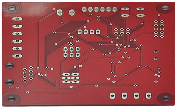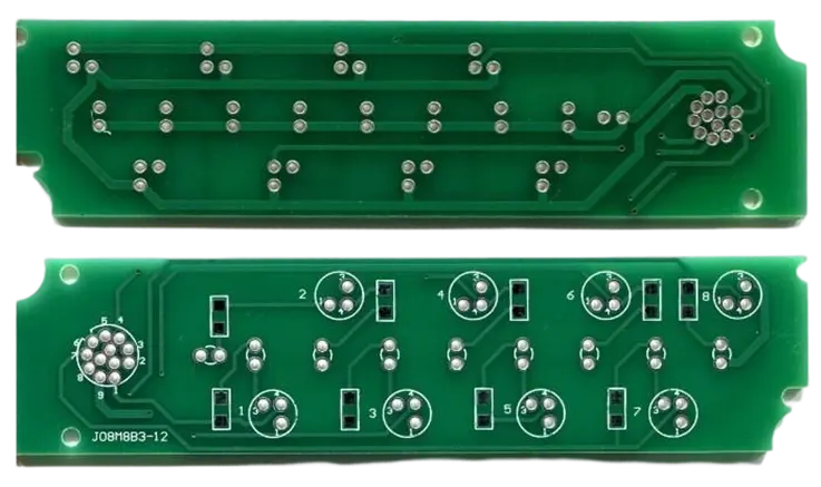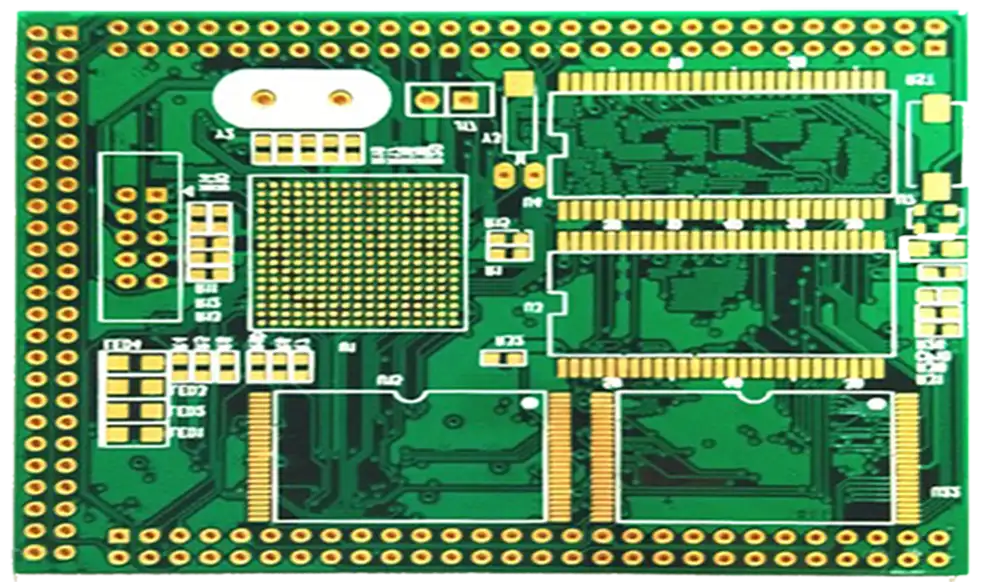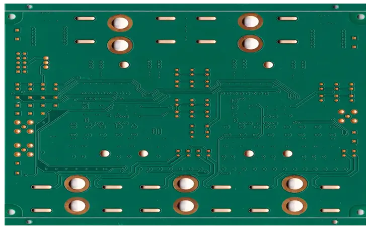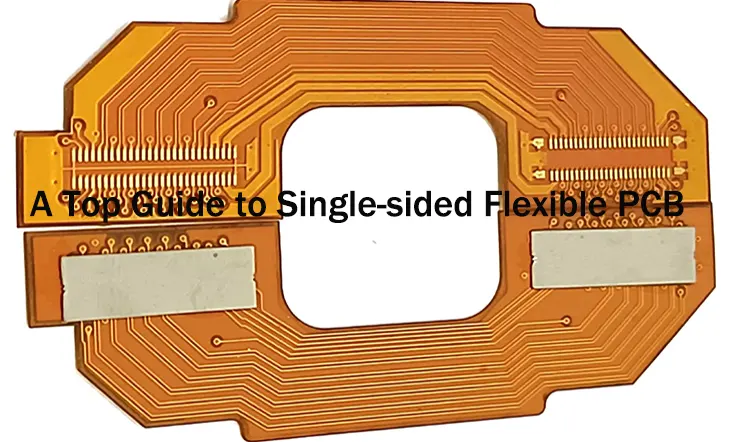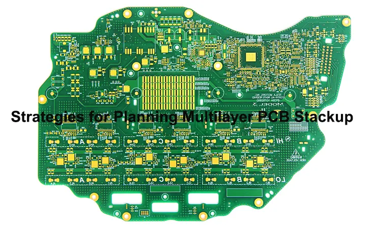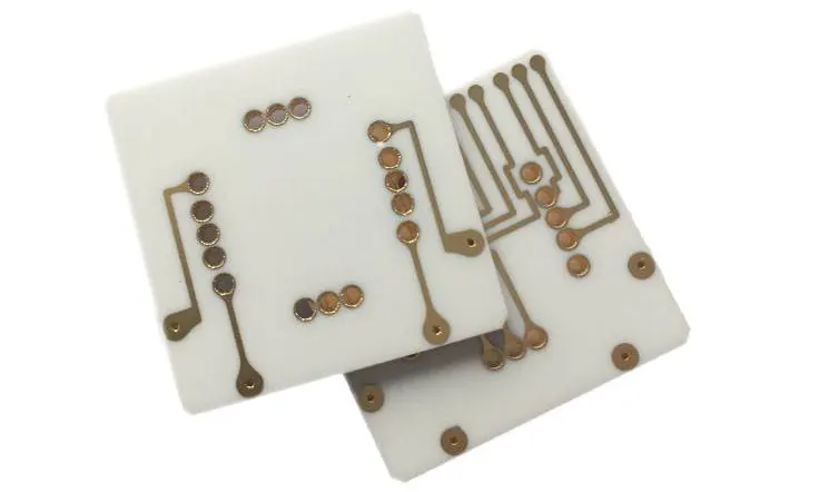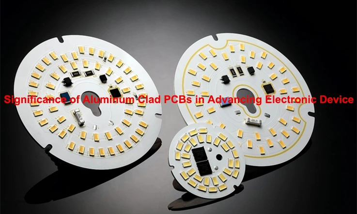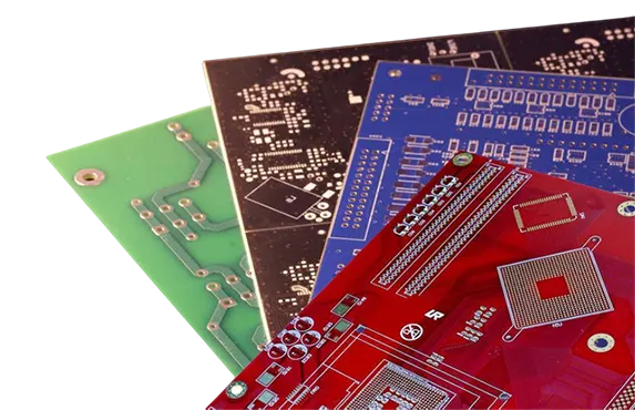
Rigid printed circuit boards (PCBs) are the heart and soul of countless devices, offering the durability and performance needed to keep modern technology moving forward. From precision medical equipment that saves lives to automotive systems that put reliability in the driver’s seat, these boards provide the structural stability required for even the most demanding applications. Their tough construction and ability to house intricate circuitry make them a go-to option for engineers and tech enthusiasts alike.
This comprehensive guide peels back the layers on rigid PCBs, exploring their nuanced design process, material choices, and advanced manufacturing techniques. Unlike flexible or rigid-flex counterparts, rigid PCBs excel when high stability and robust performance are non-negotiable. For example, in high-frequency systems or devices operating in harsh environments, these boards shine with precision and resilience.
Through this journey, you’ll uncover how the integration of advanced materials like FR-4 and ceramic laminates, coupled with cutting-edge fabrication methods, caters to diverse needs—from high-speed communications to aerospace-grade electronics. Paired with easy-to-follow tables and case studies, this guide provides the insights needed to navigate the world of rigid PCBs confidently. So roll up your sleeves, and let’s tackle this topic with all the gusto it deserves!
Introduction to Rigid PCB: What Every Electronics Manufacturer Should Know?
When designing or manufacturing electronic devices, one of the first things that comes to mind is the Printed Circuit Board. Among the different types of PCBs, rigid PCBs are the most commonly used in a wide range of applications. But what makes them the go-to choice for electronics manufacturers? This section dives deep into the basics of rigid PCBs, how they contribute to the performance of various devices, and why they should be considered an integral part of your manufacturing process.
What is a Rigid PCB and Why is it Important in Electronics?
At its core, a rigid PCB is a type of printed circuit board that is made from a solid, inflexible material—typically fiberglass or a similar material that gives it a robust, durable structure. These rigid boards are designed to house electronic components like resistors, capacitors, and integrated circuits, connecting them together with copper pathways. This is what makes them so crucial in electronic devices—they not only provide mechanical support, but also guide electrical connections, ensuring everything works in harmony.
But why is this rigid PCB so highly regarded in the electronics industry?Rigid PCBs deliver unmatched stability. In scenarios demanding precision—such as consumer electronics, automotive systems, and medical devices—they provide a reliable, unyielding foundation for maintaining performance. Unlike flexible boards that accommodate bending, rigid designs firmly secure components, reducing the chance of damage or signal disruption from movement or mechanical stress.
For example, in smartphones or laptops, the rigid PCB ensures that all components like processors and memory chips stay securely connected, even with constant handling. Without a solid foundation, these devices wouldn’t function as expected.
Think of it as the spine of your device—everything else connects to it, and without it, your circuits would just fall apart.
| Component | Material | Function | Examples |
| Base Material | Fiberglass/Epoxy | Provides rigidity, durability, and insulation | FR-4, Polyimide |
| Copper Layer | Copper | Electrical pathways for circuits | Single-sided PCB |
| Components | Various | Resistors, capacitors, ICs, etc. | Smartphones, TVs |
The combination of these materials ensures that rigid PCBs provide excellent mechanical stability and electrical integrity for a variety of applications, from smartphones to automobiles.
The Key Advantages of Rigid PCBs for Electronics Manufacturing
When it comes to manufacturing rigid PCBs, a few key advantages set them apart from other types of boards like flex PCBs or multilayer PCBs. Let’s break these down:
●Reliability: One of the biggest reasons why rigid PCBs are preferred is their reliability. Their solid structure makes them less susceptible to damage from external forces, ensuring that the electronic circuits they support maintain their functionality. This makes them ideal for use in products that demand high reliability, such as automotive electronics, medical devices, and industrial equipment.
●Cost-effectiveness: In terms of production, rigid PCBs are often more cost-effective compared to flexible boards. The simplicity of the design and the widespread availability of manufacturing processes make them a more affordable option for mass production. For businesses looking to keep costs low without sacrificing quality, rigid PCBs are a smart choice.
●Design Flexibility: Despite being “rigid,” these boards can still accommodate complex circuit designs. With the ability to support single-layer, double-layer, and even multilayer PCB designs, rigid boards offer plenty of flexibility in terms of electrical performance, meeting the unique needs of electronics manufacturers.
| Advantage | Description | Example Applications |
| Reliability | Strong and stable design makes them less prone to physical damage. | Automotive Electronics, LED lights |
| Cost-effectiveness | Lower manufacturing costs due to simple design and materials. | Consumer Electronics |
| Design Flexibility | Flexible circuit layouts for multi-layer designs and complex needs. | Medical Devices, Smart Devices |
For example, in the automotive industry, rigid PCBs are used to control a car’s engine management system. The stability and reliability of the board ensure that the system can manage complex tasks like fuel injection timing and exhaust control, contributing to optimal engine performance.
Overview of Rigid PCB Materials and Their Role in Performance
Choosing the right material for a rigid PCB is a lot like picking out the right materials for a construction project—not all materials are created equal. Here’s a breakdown of the most popular materials used in rigid PCB manufacturing and what they bring to the table.
●FR-4: FR-4 is the most widely used material for rigid PCBs. It’s a type of fiberglass-reinforced epoxy laminate that offers great mechanical strength and thermal stability. FR-4 is affordable, easy to manufacture, and provides excellent dielectric properties, making it a go-to choice for most general-purpose PCBs.
●Polyimide: For applications where high temperature resistance is required, polyimide is a go-to option. This material is often used for flexible PCBs, but it can also be incorporated into rigid PCBs that need to withstand extreme heat. Its high thermal stability makes it ideal for applications like aviation and military electronics, where performance in harsh environments is a must.
●CEM1 and CEM3: These materials are used in applications where cost-effective solutions are needed without compromising too much on performance. CEM1 is a composite material that provides a good balance between electrical performance and cost, while CEM3 is slightly more advanced, offering better mechanical properties.
Material choice hinges on factors like thermal conductivity and electrical performance, tailored to the needs of specific applications. For instance, in power electronics, where managing heat is a priority, ceramic-based PCBs often take the spotlight due to their superior ability to dissipate heat. On the flip side, consumer devices, which prioritize affordability and scalability for mass production, lean heavily on FR-4 material, striking a balance between cost-effectiveness and functionality.
Here’s a quick look at how material choice affects rigid PCB performance:
| Material | Thermal Conductivity | Electrical Properties | Cost |
| FR-4 | Medium | High | Low |
| Polyimide | High | High | High |
| CEM1 | Medium | Medium | Low |
| CEM3 | Medium | High | Medium |
Rigid PCB Design: The Process and Key Considerations
Designing a rigid PCB involves more than just laying down a few traces. It’s a meticulous process that includes signal integrity management, careful layer stack-up considerations, impedance control, and exact component placement. These are critical elements that ensure the PCB will perform reliably across a variety of demanding applications. In this section, we’ll discuss the process in depth, along with the challenges you’ll face and the solutions to overcome them.
Understanding the Rigid PCB Design Process
A rigid PCB design doesn’t start with components or traces. It begins with defining the electrical characteristics that need to be preserved, followed by a series of strategic decisions to optimize layout and electromagnetic compatibility (EMC).
1.Signal Integrity & Impedance Control: Signal integrity refers to the quality of the electrical signals traveling through the PCB’s traces. For high-speed signal design, achieving proper impedance control is paramount. Impedance mismatches can result in signal reflections, crosstalk, and data corruption. Using tools like finite element analysis (FEA) or electromagnetic field solvers to simulate signal paths and impedance is a must.
For example, the FR4 material (the standard in PCB manufacturing) can be used for most consumer applications, but it’s not always the best for high-speed circuits. Specialized materials like Polyimide or PTFE might be necessary to achieve better signal quality and reduce losses due to dielectric constant discrepancies.
| Design Consideration | Example Materials | Signal Integrity Impact | Best Practices |
| Impedance Control | FR4, Polyimide, PTFE | Maintains stable signal integrity | Use simulation tools and controlled impedance trace widths |
| Signal Trace Width | Copper, Gold | Affects current capacity and loss | Use CAD tools to optimize trace dimensions |
| Electromagnetic Shielding | Conductive materials | Prevents signal leakage | Place ground planes close to traces |
2.Layer Stack-Up: The stack-up is the arrangement of copper and dielectric layers within the PCB. A well-designed stack-up balances layer count, trace routing, and signal interference management. For multi-layer rigid PCBs, controlling stack-up balance helps prevent issues like warping and ensures that high-frequency signals remain unaffected by noise.
Challenges in Rigid PCB Design: Solutions for Common Issues
As with any complex engineering project, designing rigid PCBs comes with its share of challenges. Let’s break down some common design issues and explore practical solutions for each.
1.Thermal Management: One of the major challenges in PCB design is managing heat, especially for high-power applications. Heat buildup in components can affect performance and potentially lead to thermal runaway if not controlled properly.
●Solution: Incorporating thermal vias, copper pour areas, and heat sinks into the design allows for efficient heat dissipation. Thermal vias act as conductive pathways, transferring heat from components to the opposite layers of the board, while copper pours help distribute the heat evenly across the PCB surface.
| Thermal Design Challenge | Impact | Design Solution | Best Practices |
| Heat Generation | Component failure, signal degradation | Use thermal vias and heat sinks | Place components in thermally optimized zones |
| Thermal Cycling | Board warping, component stress | Add copper pours and thermal management materials | Use high-thermal-conductivity materials |
2.Cross-talk and Electromagnetic Interference (EMI): Cross-talk occurs when electrical signals in one trace interfere with adjacent traces. With high-frequency designs, the risk of EMI is especially high, leading to unreliable performance.
●Solution: To keep electromagnetic interference (EMI) at bay, you can sandwich ground planes between sensitive signal traces, creating a shielded pathway that reduces noise. Adjusting trace width and spacing ensures proper impedance matching and helps maintain signal clarity. Adding shielding or guard traces around high-priority signals acts like a buffer, keeping unwanted interference at a safe distance and letting your circuit do its thing without a hitch.
| Issue | Symptoms | Solution | Design Tips |
| Cross-Talk | Signal interference, distorted data | Add ground planes and guard traces | Ensure trace spacing complies with IPC standards |
| Electromagnetic Interference (EMI) | Reduced signal integrity and performance | Use shielding, ground planes, and signal routing techniques | Twist signal traces to cancel out noise effects |
Designing Multilayer Rigid PCBs for Complex Applications
Multilayer rigid PCBs are widely used in complex, high-density electronic systems. These include everything from mobile phones to advanced medical devices and automotive electronics. The increased layer count allows for greater component density and more efficient routing. But this also means more design complexity.
1.High-Density Interconnects (HDI): As component sizes shrink, the need for HDI designs increases. HDI PCBs use advanced manufacturing techniques like laser drilling, blind and buried vias, and microvias to allow for more layers in a compact space. High-density routing ensures that components are placed efficiently without sacrificing performance or reliability.
2.Balancing Cost and Performance: With more layers, the cost of production increases. The challenge is to balance performance needs with budget constraints. Designers need to optimize the number of layers based on functional requirements while keeping production costs in check.
| HDI Design Challenge | Impact | Solution | Best Practices |
| High-Density Routing | Complicated routing, limited space | Use laser vias, microvias, and advanced layer stack-ups | Use via-in-pad and stacked vias |
| Cost vs. Performance | Increased production costs | Optimize the layer count and materials | Use simulation tools to balance cost/performance |
Rigid PCB Manufacturing: From Design to Finished Product
The rigid PCB manufacturing process is a multifaceted journey that takes the PCB design from a schematic to a fully functional printed circuit board, ready for deployment in electronic devices. Understanding the intricacies of the entire fabrication process, the options available for surface finishing, and the various quality control methods used during production will help electronics manufacturers produce reliable and high-performance rigid PCBs.
The Rigid PCB Fabrication Process: Key Stages
The rigid PCB fabrication process involves several stages that require precision and high-quality equipment. Let’s break down the key stages of this process to ensure a clear understanding.
1.Etching and Layer Lamination: The first major step in the fabrication process involves etching the copper layer on the PCB, which will form the circuit traces. The unwanted copper is removed, leaving the desired pattern for electrical connections. If the PCB is a multilayer design, lamination comes into play. This process fuses the copper and dielectric layers together, creating a sturdy structure that will handle the electrical and mechanical stresses during usage.
2.Drilling and Vias: Drilling is a necessary step for creating holes through the PCB for component leads, connectors, and vias—the electrical connections between layers of the PCB. These vias can either be through-hole vias (connecting all layers) or blind vias (extending only to certain layers). Precision during drilling directly impacts the functionality of the board, as even a minor misalignment or incorrect hole size can disrupt electrical continuity or degrade signal transmission. This step relies heavily on advanced equipment and careful calibration to ensure that all layers align seamlessly and that every hole meets exact specifications, avoiding costly errors or rework.
3.Solder Mask Application and Silkscreen Printing: Applying a solder mask to the PCB serves as a protective layer that prevents the copper traces from oxidizing and restricts solder application to specific areas during assembly. This process not only safeguards the circuit’s integrity but also helps avoid unintended electrical connections. Following this, silkscreen printing adds crucial visual markers to the board, such as component labels and reference designators. These markings guide technicians during assembly and maintenance, streamlining the identification of components and circuits. Together, these steps enhance the functionality and usability of the PCB, ensuring smooth manufacturing and troubleshooting processes.
4.Plating and Surface Finishing: The next step in the PCB manufacturing process is plating, where copper plating is applied to the holes and the edges of the PCB. This ensures proper electrical conductivity. After plating, the surface finish is applied to the exposed copper pads to protect them from corrosion and to ensure solderability. The choice of surface finish—HASL, ENIG, OSP, or immersion silver—affects the board’s performance and longevity.
| Fabrication Stage | Description | Material Used | Impact on Performance |
| Etching | Removes unwanted copper to form conductive traces | FR4, Polyimide | Ensures precise trace dimensions |
| Layer Lamination | Layers copper and dielectric to create multilayer board | FR4, CEM1 | Strong electrical connections between layers |
| Drilling & Vias | Creates holes for component leads and inter-layer connections | Copper, FR4 | Affects PCB strength and connectivity |
| Solder Mask & Silkscreen | Adds protective coating and prints component markings | Epoxy, Ink | Improves soldering and board readability |
5.Final Assembly and Inspection: After fabrication, the final assembly and testing of the board take place. In this step, automated optical inspection (AOI) and X-ray inspection ensure that no defects exist in the PCB. Electrical testing is also performed to verify the functionality of the board.
Surface Finishing for Rigid PCBs: Choosing the Right Method
The surface finish of a rigid PCB directly influences its solderability, protection against corrosion, and how well it maintains electrical performance. Different finishing methods cater to specific needs—whether prioritizing cost-efficiency, longevity, or compatibility with high-frequency signals.
1.HASL (Hot Air Solder Leveling): HASL is the most commonly used surface finish for rigid PCBs due to its cost-effectiveness. The HASL process involves applying a thin layer of solder to the PCB pads. It’s widely used in low- to mid-volume production but can lead to uneven finishes and issues with fine-pitch components. As PCBs become smaller and more complex, HASL is less ideal for high-density interconnect (HDI) designs.
2.ENIG (Electroless Nickel Immersion Gold): ENIG is widely considered the gold standard for rigid PCBs that require high-reliability. The ENIG process deposits a thin layer of nickel and gold on the PCB pads. This finish provides a flat surface, ensuring consistent solderability for fine-pitch components. It also has excellent corrosion resistance and is ideal for lead-free soldering applications.
3.OSP (Organic Solderability Preservative): The OSP finish is a newer, environmentally-friendly option. This method involves applying an organic coating to the copper to protect it from oxidation. While OSP is cost-effective and suitable for low-volume production, it does not provide the same level of protection as HASL or ENIG, particularly in harsh environments.
4.Immersion Silver: Immersion silver is a surface finish known for providing a smooth, even coating that supports excellent soldering and is particularly suitable for high-density designs. By depositing a thin silver layer over the copper pads, this method ensures a flat surface that meets the stringent requirements of HDI (High-Density Interconnect) PCBs. Its lead-free compatibility makes it a popular choice for environmentally conscious manufacturing processes. Additionally, immersion silver offers strong performance in maintaining signal integrity, making it ideal for high-frequency applications.
| Surface Finish | Characteristics | Applications | Advantages |
| HASL | Solder applied with hot air leveling | Budget designs, mass production | Low-cost, good for large-scale production |
| ENIG | Nickel and gold plating | High-reliability, fine-pitch components | Flat, corrosion-resistant, lead-free soldering |
| OSP | Organic coating for solderability | Eco-friendly designs | Environmentally friendly, cost-effective |
| Immersion Silver | Thin silver layer | Lead-free solder, high-density designs | Excellent solderability, flat surface |
Quality Control in Rigid PCB Manufacturing
Manufacturing rigid PCBs requires stringent quality control measures to ensure reliability. From the blueprint phase to the final stages of assembly, each step undergoes a series of precise tests to catch any hitches before the board sees action in its intended device. This process ensures that potential snags like connectivity faults, layer misalignments, or soldering issues are ironed out, keeping the board’s performance up to scratch.
1.Automated Optical Inspection (AOI): AOI is the most widely used method for visual inspection of PCBs. It uses high-resolution cameras to inspect the solder joints, trace alignments, and other critical aspects of the PCB. AOI can be automated to check for misalignment, open circuits, and soldering defects, offering quick feedback during the fabrication process.
2.X-ray Inspection: For high-density multilayer PCBs, especially those featuring intricate internal layers, X-ray inspection is a go-to method for spotting hidden issues like misaligned vias or gaps in solder joints. This approach enables a detailed, non-invasive review of the PCB’s internal structure, revealing flaws that might otherwise go unnoticed. It’s particularly useful for HDI boards, where precision in buried or blind vias is a must.
3.Electrical Testing: This is the final step to ensure the rigid PCB works as intended. Electrical testing checks for short circuits, open circuits, and signal integrity issues. Flying probe testers or bed-of-nails testers are used to verify the electrical functionality of the board before it is shipped for final assembly.
4.Certifications and Standards: Compliance with ISO 9001, IPC-2221, and other international standards ensures that the PCB manufacturer meets the highest quality requirements. Certifications also indicate that the manufacturer follows standardized procedures, which ensures that the final product is both reliable and durable.
| Quality Control Method | Purpose | Test Equipment | Benefits |
| AOI | Identifies visual defects such as misalignment | Automated optical inspection systems | High-speed inspection, early detection of defects |
| X-ray Inspection | Checks internal layers for defects | X-ray machines | Inspect hidden layers for alignment issues |
| Electrical Testing | Ensures connectivity and signal integrity | Flying probes, bed-of-nails testers | Validates performance and signal paths |
| Certifications | Verifies adherence to global standards | Certification audits | Ensures reliability, compliance with industry standards |
Materials for Rigid PCB Manufacturing: Optimizing Performance
When it comes to rigid PCB manufacturing, the choice of materials isn’t something to take lightly. It’s one of the most important factors that directly influences the performance, cost, and durability of your PCB. Whether you’re designing for consumer electronics, automotive applications, or high-frequency systems, selecting the right material is key to ensuring that your circuit boards meet the specific needs of your product. Let’s dive deeper into some of the most popular and high-performance materials used in rigid PCB manufacturing.
The Role of FR-4 and Other Common PCB Materials
FR-4 is the go-to material for the vast majority of rigid PCBs. But what makes it such a reliable and popular choice? Well, FR-4 is a glass-reinforced epoxy laminate, and it stands out for its combination of affordability, electrical properties, and mechanical strength. In fact, its widespread adoption in the electronics industry is a testament to its performance across a wide range of applications. But hey, it’s not the only game in town—let’s explore some other materials.
Why FR-4 Dominates the Market-
●Cost-Effectiveness: If you’re looking for a material that balances cost and performance, FR-4 is your best bet. It’s not only widely available, but also a budget-friendly option for large-scale production.
●Durability: With excellent mechanical strength and resistance to environmental factors, FR-4 makes for a sturdy PCB that can stand up to the rigors of consumer electronics.
●Thermal Properties: While it’s great for most applications, FR-4 may not always be the best choice for high-frequency or high-power systems where thermal management becomes a priority. For these cases, there are alternative materials worth considering.
Other PCB Materials-
●Polyimide: A flexible material often used in flexible PCBs, polyimide also finds its way into rigid PCBs when flexibility and thermal stability are needed for specialized applications.
●Ceramics: Known for their superior thermal conductivity, ceramics are the go-to material for high-frequency applications and products requiring excellent heat dissipation.
●Teflon: This high-performance material excels in high-frequency applications, making it a solid choice for microwave circuits and other applications requiring minimal signal loss.
Key materials used in rigid PCB manufacturing:
| Material | Pros | Cons | Applications |
| FR-4 | Cost-effective, durable, widely used | Poor thermal management in high power | Consumer electronics, computers |
| Polyimide | Flexible, good thermal properties | Expensive compared to FR-4 | Flexible PCBs, high-temperature apps |
| Ceramics | High thermal conductivity, stable | Expensive, complex to manufacture | High-frequency, aerospace, automotive |
| Teflon | Low signal loss, high-frequency stability | Expensive, difficult to process | Microwave circuits, RF applications |
Thermal Management in Rigid PCBs: Materials That Matter
Effective thermal management is the backbone of maintaining both the durability and functionality of rigid PCBs. With electronic components becoming increasingly compact and powerful, heat buildup can no longer be overlooked. Proper handling of heat dissipation ensures the components don’t overheat or degrade over time. Choosing materials with high thermal conductivity, integrating heat sinks, or employing thermal vias are just a few strategies to keep temperatures in check. Without these measures, even the most sophisticated PCB designs could falter, leading to performance hiccups or shortened lifespan. Handling heat isn’t just smart—it’s necessary for success in today’s tech-driven designs.
How Materials Impact Thermal Performance-
●Copper Thickness: Boosting the thickness of copper in PCB traces is a go-to strategy for enhancing thermal management. Thicker copper layers handle higher current loads, cutting down on resistance and minimizing the heat produced during operation. This approach is particularly handy for applications like power supplies or LED drivers, where components often demand more power. The added thickness also provides extra durability, making it a solid choice for boards exposed to high stress or harsh environments. It’s all about finding that sweet spot between performance and durability, ensuring your design can handle the heat without breaking a sweat.
●Thermal Vias: These are small channels drilled through the PCB that connect different layers, allowing heat to travel efficiently between them. By strategically placing thermal vias, the heat generated by components can be distributed more evenly, preventing hotspots.
Key Materials for Effective Thermal Management-
●Aluminum: Often used in power PCBs, aluminum is a fantastic conductor of heat and is commonly used when designing PCBs that need to handle large power loads without excessive heat buildup.
●Copper-Clad PCBs: The use of thicker copper layers in your PCB stack-up is an excellent way to improve thermal conductivity and enhance overall performance.
●Ceramic PCBs: For applications with extremely high heat dissipation requirements, ceramic-filled PCBs are the go-to choice. They can withstand extreme temperature changes without affecting the integrity of the PCB.
Let’s break down thermal management materials in the table below:
| Material | Benefits | Ideal Use Case |
| Aluminum | Excellent heat dissipation, lightweight | Power PCBs, LED applications |
| Copper | Good thermal conductivity, versatile | High-power PCBs, automotive electronics |
| Ceramic-filled PCBs | Best for high-frequency, high-heat scenarios | Aerospace, military, high-power applications |
Choosing High-Performance Materials for Rigid PCBs
For certain industries like military, aerospace, and automotive, the performance demands of a rigid PCB go through the roof. In these cases, standard materials like FR-4 just won’t cut it. High-performance materials are required to meet the strict performance standards for these applications.
High-Performance Material Options-
●Ceramic-Filled Composites: These are used for high-frequency and high-power applications. They can handle higher temperatures and have much better thermal conductivity than traditional materials.
●High-Frequency Laminates: Materials like Rogers or Arlon are ideal for high-frequency PCBs because they minimize signal loss and ensure that data travels without delay. These laminates have low dielectric constants and low loss tangents, making them perfect for RF and microwave applications.
●Polyimide: Not only is polyimide flexible, but it also offers excellent thermal stability and resistance to high temperatures. It’s the go-to material for any aerospace or military applications where performance must be ensured in extreme conditions.
Case Study Example:
Let’s take a military-grade PCB designed for an avionics system. To withstand the high temperatures and electrical stresses of the aircraft’s environment, designers often choose a combination of ceramic-filled composites and high-frequency laminates. This ensures the PCB performs optimally, even under extreme pressure.
High-performance materials for specialized applications:
| Material | Advantages | Best Suited For |
| Ceramic-filled Composites | Excellent thermal performance, high durability | Military, aerospace, high-power applications |
| High-frequency Laminates | Low signal loss, high-frequency stability | RF, telecommunications, microwave systems |
| Polyimide | Flexible, thermal stability | Aerospace, automotive, high-temperature applications |
Types of Rigid PCBs: Selecting the Right Type for Your Application
Rigid PCBs are the backbone of countless electronic devices, offering mechanical stability and efficient routing for complex circuitry. However, choosing the right type of rigid PCB for your project can feel like navigating a maze. Do you need a simple single-layer design, a multilayer setup for dense circuits, or a hybrid rigid-flex approach? Let’s break down the types of rigid PCBs, their advantages, and the factors to consider in your selection.
Single-Sided vs. Double-Sided Rigid PCBs: Which One to Choose?
Single-sided rigid PCBs are as straightforward as they come—one conductive layer on one side of the board. They’re commonly found in simple, cost-sensitive applications like calculators, power supplies, and LED lighting. On the flip side, double-sided PCBs have conductive layers on both sides, doubling the real estate for routing and opening the door to more complex designs.
Key Applications for Single-Sided and Double-Sided Rigid PCBs-
●Single-sided PCBs: Ideal for cost-conscious products with low component counts, such as household appliances or battery chargers.
●Double-sided PCBs: Often used in applications requiring greater complexity, like industrial controls, HVAC systems, and low-cost IoT devices.
The Trade-Offs: Simplicity vs. Complexity
| Feature | Single-Sided PCBs | Double-Sided PCBs |
| Cost | Low cost due to simple manufacturing | Moderate cost due to extra processing |
| Complexity | Limited routing, no through-hole connections | Enhanced routing with vias available |
| Common Uses | Basic gadgets, LED lights | Consumer electronics, power devices |
| Design Flexibility | Minimal, suitable for basic designs | Higher flexibility for more complex setups |
Multilayer Rigid PCBs: Advantages for Complex Designs
When simple boards can’t handle the pressure, multilayer PCBs step up to the plate. These boards sandwich multiple conductive layers between insulating materials, offering a compact yet powerful solution for designs with heavy interconnect demands. Think of multilayer PCBs as the skyscrapers of the PCB world—they build up instead of spreading out.
Why Multilayer Rigid PCBs Shine-
●High-Density Interconnects (HDI): With multiple layers to work with, designers can create dense, high-performance circuits without increasing the board’s footprint.
●Signal Integrity: The layered design makes it easier to manage EMI (electromagnetic interference) and maintain signal quality, even in high-speed applications.
Applications for Multilayer Rigid PCBs-
●Automotive Electronics: From advanced driver-assistance systems (ADAS) to infotainment systems, multilayer PCBs handle the complexity and compactness required in modern vehicles.
●Medical Devices: High-performance diagnostic tools and portable medical devices often rely on multilayer designs for their precision circuitry.
●Telecommunications: Routers, switches, and high-frequency communication systems benefit from multilayer boards’ ability to support multiple signals simultaneously.
Managing Signal Integrity in Multilayer Designs-
One challenge with multilayer boards is maintaining signal integrity in the face of high-speed data transfers. Designers can mitigate issues like crosstalk and reflection by carefully planning layer stack-ups and using proper shielding techniques.
Layer Stack-Up Example:
| Layer Type | Function |
| Top Layer | Signal layer |
| Inner Layer 1 | Power distribution |
| Inner Layer 2 | Ground plane for EMI reduction |
| Bottom Layer | Signal layer |
Rigid-Flex PCBs: Combining Flexibility and Rigid Structures
Rigid-flex PCBs are the Swiss Army knife of circuit boards. They combine rigid sections for mounting components with flexible sections for tight spaces or dynamic movements. This versatility makes them a favorite in industries like wearables, automotive, and medical devices, where compactness and adaptability are prized.
Benefits of Rigid-Flex PCBs-
●Compact Design: By eliminating bulky connectors and cables, rigid-flex boards save space and reduce overall assembly weight.
●Improved Durability: Flexible sections are better at absorbing mechanical stress, making these boards suitable for applications involving movement or vibration.
Industries That Love Rigid-Flex Designs-
●Automotive: Think of wiring harness replacements in modern cars, where space is at a premium but reliability is non-negotiable.
●Wearables: Smartwatches and fitness trackers leverage rigid-flex PCBs for their compact, ergonomic designs.
●Medical Devices: Hearing aids and implantable devices require the reliability and form factor that rigid-flex boards provide.
Design and Manufacturing Considerations-
While rigid-flex boards are a marvel of modern engineering, designing them requires careful attention to detail:
●Bend Radius: Flexible sections must adhere to specific bend radius guidelines to prevent damage.
●Material Selection: Polyimide is often used for the flexible layers due to its durability and heat resistance.
Here’s a look at the trade-offs involved in rigid-flex PCB design:
| Feature | Advantages | Considerations |
| Space Efficiency | Excellent for tight spaces | Requires precise design and assembly |
| Cost | Reduces overall system cost | Higher initial manufacturing costs |
| Reliability | Fewer connectors improve durability | May require specialized testing |
High-Speed and High-Frequency Rigid PCB Design
As electronic devices push the boundaries of speed and frequency, designing rigid PCBs for high-performance systems requires a mix of precision, advanced materials, and engineering prowess. From 5G networks to satellite communication systems, high-speed and high-frequency PCB designs play a pivotal role in achieving peak performance while minimizing losses.
Challenges in High-Speed Rigid PCB Design
High-speed signals introduce challenges that designers cannot ignore. With increasing frequencies, the once-minor effects of parasitics, crosstalk, and impedance mismatches can wreak havoc on performance. Addressing these challenges involves an understanding of signal behavior, material properties, and layout strategies.
Key Challenges and Solutions-
1.Signal Integrity Management: High-speed signals are prone to distortions such as reflections and attenuation. To combat these issues:
●Use controlled impedance traces: Ensuring that signal paths maintain a consistent impedance reduces reflection and maintains signal quality.
●Include return paths with ground planes: Continuous ground planes provide an unbroken path for current return, minimizing inductance and noise.
●Employ differential pairs: For high-speed differential signals, closely spaced trace pairs can reduce common-mode noise.
2.Crosstalk and EMI (Electromagnetic Interference): Signals traveling through adjacent traces can interfere with each other. Here’s how to mitigate these effects:
●Maintain adequate trace spacing to minimize coupling between signal paths.
●Introduce shielding layers to protect sensitive traces from external noise.
3.Thermal Management: Heat dissipation becomes a concern as signal frequencies rise, especially in dense designs.
●Utilize thermal vias and copper pours to spread heat effectively.
●Consider heat sinks or thermal pads for components generating significant heat.
Solutions to High-Speed Design Challenges:
| Challenge | Impact | Solution |
| Signal Integrity | Reflections, distortion, attenuation | Controlled impedance, ground planes |
| Crosstalk and EMI | Signal degradation, noise interference | Trace spacing, shielding, differential pairs |
| Thermal Management | Component overheating, reduced lifespan | Thermal vias, heat sinks, copper pours |
Materials for High-Frequency Rigid PCBs
When working with high-frequency designs, choosing the right materials can determine the success of your project. You need materials that maintain steady dielectric properties, low loss tangents, and top-notch thermal performance. These factors are key when you’re aiming to handle GHz-range frequencies without compromising signal integrity. Using the wrong material can cause significant signal degradation, especially at higher frequencies, so selecting a material that can perform under these conditions is a no-brainer. It’s like picking the right gear for a race—if your equipment can’t handle the demands, you’re going to fall behind.
Popular Materials and Their Properties-
1.PTFE (Polytetrafluoroethylene): Known for its low loss tangent and high thermal stability, PTFE is ideal for microwave and RF applications. Its downside is the complexity and cost associated with processing.
●Applications: Radar systems, satellite communications, and 5G base stations.
2.Teflon: Often used interchangeably with PTFE, Teflon laminates offer low dielectric constants and high-frequency stability.
●Advantages: Outstanding performance in RF circuits and reduced signal loss.
●Drawbacks: Higher cost and specialized manufacturing requirements.
3.Ceramic-Filled Composites: These materials combine the benefits of ceramics and polymers, providing excellent thermal conductivity and mechanical strength. They are particularly effective in high-power RF and microwave designs.
4.High-Frequency Laminates (e.g., Rogers 4350B): Engineered for superior electrical performance, these laminates ensure consistent performance at high frequencies and are easier to process compared to PTFE.
Material Comparison Table
| Material | Dielectric Constant (Dk) | Loss Tangent | Applications |
| PTFE | ~2.1 | Very low | Microwave circuits, 5G networks |
| Ceramic-Filled | 3-10 (varies) | Low | High-power RF, radar systems |
| Rogers 4350B | ~3.48 | Low | High-frequency multilayer designs |
Why Material Selection Matters in High-Speed Designs?
Choosing the right material is about balancing electrical, thermal, and mechanical properties. For instance, a 5G network node demands low-loss laminates to maintain signal clarity across multiple GHz, while a radar system may prioritize thermal stability under high-power operation.
Pro Tip: Material selection can significantly impact production costs and assembly methods. For example, PTFE boards may require advanced processing techniques, while Rogers laminates offer easier handling but at a premium price.
Why Choose Us to Manufacture Your Rigid PCBs?
At JarnisTech, we don’t just produce PCBs; we bring your ideas to life with unmatched precision and expertise. Whether you need a straightforward single-layer board or a complex, high-performance 60-layer multilayer design, we have the technical know-how and resources to deliver top-notch results. If you’re uncertain about the best solution for your project, our dedicated overseas sales team is ready to guide you every step of the way. We pride ourselves on turning challenges into opportunities, ensuring your requirements are met with precision and efficiency.
Our Capabilities: Rigid PCBs Built to Perform
We’ve invested heavily in advanced technology and stringent quality control measures to deliver rigid PCBs that exceed expectations. Our extensive capabilities ensure your designs are not only realized but optimized for reliability and performance.
| Capability | Specification | What This Means for You |
| Trace Width/Spacing | 3-mil lines and 3-mil gaps | High-density, compact designs without compromising quality. |
| Mechanical Drill Size | Minimum 8 mil | Precision drilling for intricate components. |
| Laser Drill Size | Minimum 3 mil | Perfect for advanced microvia structures. |
| Controlled Impedance | Yes | Ensures signal integrity in high-frequency applications. |
| Via Options | Blind and Buried Vias | Reduces layer count and enhances space efficiency. |
| Certifications | ISO 9001, UL Certified | Trusted for global standards and compliance. |
| Environmental Compliance | RoHS Compliant | Eco-friendly manufacturing practices. |
Why Our Clients Choose JarnisTech?
1.End-to-End Support-
From prototyping to mass production, we offer a full suite of services designed to streamline your project. Our sales team is known for their quick turnaround on quotes and comprehensive guidance, making your experience hassle-free.
2.Advanced Manufacturing Technology-
Using state-of-the-art equipment, we can handle intricate designs and high-volume production with ease. Whether you need impedance control or specialized via technology, we’ve got you covered.
3.Unmatched Quality Assurance-
Each PCB undergoes rigorous quality control, including AOI (Automated Optical Inspection) and electrical testing, ensuring your boards meet the highest standards.
4.Flexible Solutions for Every Industry-
We cater to diverse sectors, including automotive, medical, and telecommunications. Our materials and processes are tailored to suit the specific requirements of your application.
Case Study: Efficiency in High-Density Designs
A recent project required a 20-layer rigid PCB for a telecommunications client. The design called for controlled impedance, 3-mil traces, and blind vias to meet space and performance requirements. Leveraging our advanced capabilities, we delivered the boards ahead of schedule, ensuring seamless integration into the client’s assembly line. The result? Reduced downtime and enhanced performance for their 5G network deployment.
Let’s Build Your Next Big Idea
Whether you’re looking to streamline production, elevate design complexity, or minimize costs, JarnisTech is your trusted partner in rigid PCB manufacturing. Don’t leave your next project to chance—contact us today to discuss your requirements and receive a tailored quote. Let’s make something amazing together!
FAQ about Rigid PCBs
1. Can rigid PCBs be used in extreme temperature environments?
Yes, rigid PCBs can be designed for extreme conditions. Materials like Polyimide or ceramic-filled laminates are often used in applications requiring high thermal resistance. These are ideal for aerospace, automotive, and military applications where temperature fluctuations are significant.
2. How do rigid PCBs handle mechanical stress compared to flexible PCBs?
Rigid PCBs are designed for durability in fixed installations but are less suited for applications with repetitive bending or movement. Unlike flexible PCBs, rigid boards can crack under excessive mechanical stress unless mounted securely.
3. What is the typical lead time for rigid PCB manufacturing?
The lead time for rigid PCB manufacturing varies by complexity. Single-layer boards might take 5-7 days, while multilayer boards with controlled impedance or blind vias may require 2-3 weeks, especially when custom testing is involved.
4. Are there eco-friendly options for manufacturing rigid PCBs?
Yes, eco-friendly manufacturing options include using lead-free soldering and RoHS-compliant materials. Some manufacturers also focus on recycling copper and laminates during the production process to minimize waste.
5. Can rigid PCBs support wireless charging applications?
Yes, rigid PCBs can be designed for wireless charging systems. They typically integrate copper coils and controlled impedance layers to optimize the electromagnetic fields required for energy transfer.
6. What is the difference between thermal vias and regular vias in rigid PCBs?
Thermal vias are specifically designed to transfer heat away from components by connecting to heat-dissipating layers. Regular vias are used for electrical connectivity between layers but are not optimized for heat conduction.
7. Can rigid PCBs include embedded components?
Yes, embedded components like resistors, capacitors, and even ICs can be integrated within rigid PCBs. This technique is used to reduce surface mounting requirements and enhance signal performance in high-density designs.
8. What testing standards are used to ensure the quality of rigid PCBs?
Common testing standards include IPC-A-600 for PCB acceptability and IPC-6012 for performance specifications. PCB Manufacturers also conduct electrical testing, X-ray inspections, and thermal cycling tests to validate the quality and reliability of rigid PCBs.

