The LED PCB industry is at the heart of modern electronics, driving innovation across sectors such as automotive, consumer electronics, and renewable energy systems. With the right design, manufacturing processes, and assembly techniques, LED PCBs can provide reliable, high-performance solutions for a variety of applications. This article explores every corner of LED PCBs, from their types and design principles to cutting-edge manufacturing and assembly processes.
Introduction to LED PCBs
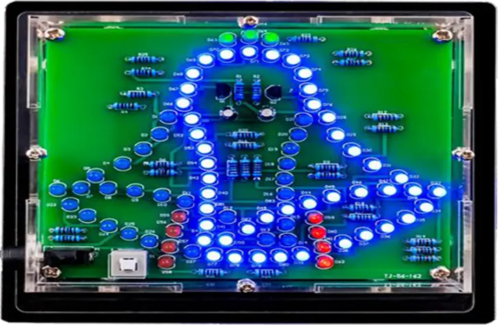
LED PCBs (Light Emitting Diode Printed Circuit Boards) represent a unique and highly efficient way to design, integrate, and power LED lighting systems. These specialized circuit boards are designed to accommodate LEDs and their unique needs, ensuring proper power distribution, heat dissipation, and durability. As industries increasingly turn to LEDs for energy-efficient solutions, LED PCBs have become an integral part of lighting technology.
LED PCBs come in various forms, such as aluminum-based, ceramic, and flexible, and each serves a distinct purpose depending on the application. Whether used in consumer electronics, automotive applications, or industrial equipment, these boards are engineered to deliver high performance, extended lifespan, and consistent light output.
The shift to LED technology has driven a demand for efficient PCB designs that can handle the high-performance nature of LEDs. With LED PCBs, designers can build more compact, durable, and sustainable products that meet the evolving needs of modern industries.
What Are LED PCBs?
LED PCBs are printed circuit boards specifically designed to house and power LED elements. Unlike regular PCBs, LED PCBs are built to handle the heat and power demands of LED lights, which can be quite intense. These PCBs are typically constructed using materials like aluminum, ceramic, and FR4 (a common fiberglass laminate), each offering different advantages based on the specific requirements of the design.
Aluminum PCBs, for example, are widely favored for their ability to dissipate heat efficiently, making them ideal for high-power LED applications like street lights and automotive lighting. On the other hand, ceramic PCBs are preferred for applications that require the utmost thermal conductivity, such as in aerospace and medical equipment. Flexible PCBs are also emerging as a trend in LED technology, enabling the creation of bendable, compact lighting solutions.
In short, LED PCBs act as the foundation for LED lights, ensuring that the LEDs receive consistent power while effectively managing the heat generated during operation. Without these specialized PCBs, LEDs would not be able to perform optimally or have the long lifespans they’re known for.
Key Benefits of LED PCBs
LED PCBs provide numerous advantages over traditional lighting solutions and other types of circuit boards, making them a go-to choice for engineers and manufacturers across a variety of industries. Let’s break down the key benefits:
1.Heat Management: As mentioned earlier, managing heat is a major factor in LED lighting efficiency. LED PCBs are designed with thermal management in mind, using high-performance materials that draw heat away from the LED chips. This helps in maintaining optimal performance while preventing overheating and potential damage. Aluminum PCBs, for example, have superior heat dissipation, allowing them to handle high-power applications that generate significant heat.
2.Energy Efficiency: LED lighting is known for its energy efficiency compared to traditional incandescent or fluorescent lights. LED PCBs optimize this benefit by ensuring that the LEDs receive the correct amount of power and function as efficiently as possible, which ultimately reduces energy consumption.
3.Durability and Longevity: One of the standout benefits of LED PCBs is their longevity. The proper thermal management and electrical characteristics ensure that LEDs remain operational for thousands of hours.
4.Compact and Flexible Designs: LED PCBs offer the flexibility to create compact, lightweight, and even flexible lighting systems. Flexible PCBs open up possibilities for unique, space-saving designs, such as wearable technology or light strips for creative displays. This adaptability has made them especially popular in consumer electronics and automotive lighting.
5.Sustainability: Compared to traditional lighting solutions, LED PCBs contribute to sustainability efforts due to their energy efficiency and long lifespan. Fewer resources are required for their production and disposal, and their energy efficiency helps reduce the carbon footprint over time.
6.Cost-Effective: While the initial investment in LED PCBs may be higher compared to traditional lighting setups, the long-term savings are significant. The reduced energy consumption, longer lifespan, and reduced need for replacements make them an economically smart choice.
Types of LED PCBs and Their Features
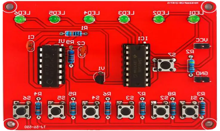
LED PCBs come in several variations, each designed for specific applications, heat dissipation requirements, and flexibility needs. Let’s dive into the three most common types of LED PCBs—Aluminum-Based, Flexible, and Ceramic PCBs—and explore how each of them meets the challenges posed by modern LED lighting solutions.
Aluminum-Based LED PCBs
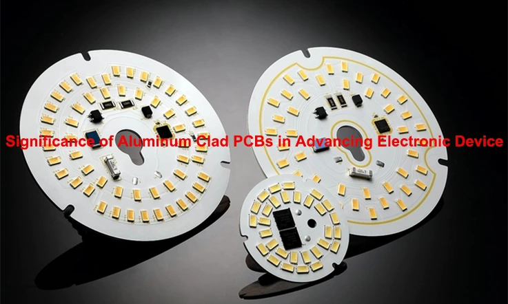
Aluminum-based LED PCBs, often referred to as aluminum PCBs, are widely used in applications where heat dissipation is a major concern. These boards feature a layer of aluminum material, typically alloyed with copper or other metals, which offers excellent thermal conductivity. This makes them perfect for high-power applications where excess heat can quickly degrade the performance of LEDs.
The aluminum substrate allows the heat generated by the LEDs to be transferred away from the chip more efficiently, reducing the risk of overheating and ensuring that the lights stay bright and last longer.
| Key Feature | Description | Best Use Cases |
| Thermal Conductivity | High thermal conductivity for managing excess heat | Automotive lighting, street lights, high-power LEDs |
| Durability | Aluminum’s sturdy and flexible properties ensure durability | Industrial lighting, outdoor signage, solar-powered lights |
| Heat Management | Excellent at transferring heat away from LED components | Power-efficient lighting systems, emergency lights |
| Cost-Effective | More affordable than ceramic alternatives | Consumer electronics, general lighting applications |
For those working in industries like automotive lighting or street lighting, aluminum-based PCBs are an absolute go-to. If you need reliable, high-performance LEDs with minimal fuss, these boards have got your back!
Flexible LED PCBs
Flexible LED PCBs are built with a flexible base material, often polyimide or PET, which allows the circuit board to bend and conform to various shapes. These types of LED PCBs are often used in applications that require lightweight, space-saving solutions that can fit into tight or irregular spaces. This makes flexible PCBs ideal for flexible lighting strips, curved displays, and wearable devices.
What sets flexible LED PCBs apart is their ability to handle complex designs in compact spaces while offering the same performance as their rigid counterparts. Plus, they come in handy when you need something that’s not just practical but also visually appealing.
| Key Feature | Description | Best Use Cases |
| Bendability | Flexible and easy to mold to different shapes and sizes | Automotive, interior lighting, signage |
| Lightweight | Ideal for portable or wearable tech | Wearable devices, smart lighting, flexible lighting strips |
| Space Efficiency | Can be mounted on curved or small surfaces | Medical devices, consumer electronics, packaging materials |
| Customization | Highly customizable to specific design needs | Custom LED strips, backlighting, compact appliances |
Flexible PCBs are making waves in the world of wearable tech and smart devices. They’re perfect for engineers looking to add LEDs to projects that need flexibility without compromising on performance. Whether it’s bending around a corner or fitting into a sleek device, flexible PCBs can get the job done.
Ceramic LED PCBs
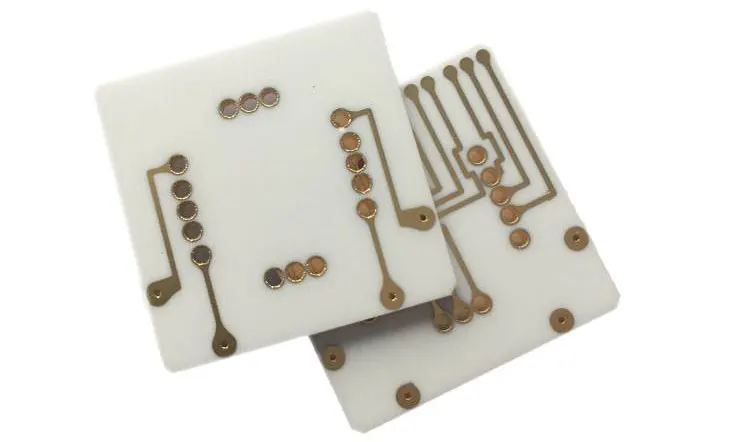
Ceramic LED PCBs are known for their high thermal conductivity and superior durability. Made from ceramic materials like aluminum nitride or boron nitride, these PCBs are ideal for applications where the management of heat is especially important. Ceramic boards also offer high resistance to oxidation and corrosion, making them ideal for harsh environments where other materials might break down.
Thanks to their high-quality build, ceramic LED PCBs are often used in applications requiring high performance and heat management, such as high-power industrial lights and LED-based medical devices.
| Key Feature | Description | Best Use Cases |
| Superior Heat Dissipation | Extremely efficient at transferring heat away from LEDs | Industrial applications, medical equipment, LED arrays |
| Corrosion Resistance | Resistant to oxidation and other environmental damage | Harsh environments, medical and military applications |
| High Reliability | Built to handle high-power applications and extended use | High-performance LED lighting, military-grade applications |
| Durability | Withstands high stress and extreme temperatures | Aerospace, automotive lighting, defense applications |
When it comes to medical devices or high-end industrial systems, ceramic LED PCBs are the top choice. They provide the durability and heat resistance needed for environments where failure simply isn’t an option. Whether it’s for a military-grade application or a specialized medical tool, these boards make sure your LEDs are running at their best.
If you’re feeling confident about choosing the right type of LED PCB for your project, why not dive deeper into the design and manufacturing process? There’s a whole world of LED possibilities just waiting for your ideas to light up!
Design Considerations for LED PCBs
Designing an LED PCB is no easy feat. It requires attention to detail, knowledge of material properties, and an understanding of how electrical components work together. Here, we’ll dive into the three key aspects of designing LED PCBs: Thermal Management, Layout Optimization, and Electrical Integrity. Each of these factors plays a role in ensuring the PCB performs optimally in real-world applications, whether that’s in your car’s lighting system, a home smart device, or medical equipment.
Thermal Management Techniques
When designing LED PCBs, one of the primary considerations is managing heat. LEDs generate a considerable amount of heat, and if not efficiently dissipated, it can damage the LED components or reduce their lifespan. Thermal management in LED PCBs is an art form, and various techniques are used to ensure longevity and performance.
A few tried-and-true methods include heat sinks, thermal vias, and advanced materials like aluminum or ceramic. Heat sinks absorb and dissipate heat, preventing it from accumulating on the board. Thermal vias are small conductive holes that allow heat to pass from the PCB’s surface to the back, where it can be safely vented.
Additionally, the material used for the PCB itself plays a huge role in thermal performance. Aluminum-based PCBs, with their high thermal conductivity, are commonly used in high-power LED applications, such as streetlights and automotive lighting. Ceramic-based PCBs are another option, offering excellent heat resistance for environments with more extreme temperatures, like industrial machines.
| Thermal Management Method | Description | Best Use Cases |
| Heat Sinks | Absorb and dissipate excess heat | High-power LEDs, street lights, automotive lighting |
| Thermal Vias | Help to transfer heat away from the LED component | Electronics with high component density, power supplies |
| Advanced PCB Materials | Utilize materials like ceramic or aluminum for better heat dissipation | High-performance applications, industrial machinery, medical devices |
Taking a more active approach to thermal management not only extends the life of your LEDs but also improves overall performance. And let’s be real: no one wants to deal with overheating, so why not do it right from the get-go?
Layout Optimization for LED Components
One of the trickiest parts of LED PCB design is figuring out how to optimize component placement. The layout must allow the LEDs to receive the proper electrical and thermal treatment while ensuring the overall system functions smoothly. Getting the layout right often requires balancing space, electrical paths, and heat dispersion.
To ensure a flawless LED performance, keep these tips in mind:
●Space between components: Overcrowding your PCB with components can create heat hotspots and may cause electrical interference. It’s best to leave ample space between components to maintain good airflow and signal integrity.
●Route traces carefully: Place traces carefully to avoid thermal bottlenecks. Long traces can also add resistance, leading to inefficiencies. Shorter, direct traces are typically better for high-current components like LEDs.
●Layer stacking: Use multi-layer PCBs to stack components and trace paths vertically. This can help improve space efficiency without compromising performance.
| Layout Tip | Description | Best Use Cases |
| Space Between Components | Ensure adequate distance to prevent heat buildup | High-density boards, high-power LED arrays |
| Short Traces | Use shorter traces to reduce resistance and heat buildup | Power-efficient designs, consumer electronics |
| Layer Stacking | Use multiple layers to save space while keeping components cool | High-performance, compact designs |
It’s all about getting that sweet spot between efficiency and performance. If your layout isn’t optimized, your LEDs will burn out quicker than you can blink. Start with a plan, and your design will be smooth sailing.
Electrical and Signal Integrity
When it comes to LED PCBs, ensuring electrical integrity means making sure the electrical signals and power supplied to the LEDs are stable and strong. Poor electrical integrity can lead to issues like flickering lights or power loss, which no one wants in their devices.
To keep the signal path clean, consider signal grounding, decoupling capacitors, and high-quality connectors. Grounding helps reduce electrical noise and prevents unintended current flow, while decoupling capacitors help smooth out power fluctuations. For those working in noise-sensitive applications, like audio-visual systems or medical devices, maintaining strong electrical integrity can make or break the performance.
Furthermore, ensuring good power distribution is key to LED PCB design. This involves careful design of the power supply network to ensure each LED receives its required voltage without excessive noise or fluctuation. If the power supply isn’t up to snuff, your LEDs might start to misbehave, flickering or even completely failing.
| Electrical Integrity Tip | Description | Best Use Cases |
| Signal Grounding | Reduces electrical noise and protects the integrity of signals | Medical devices, audio-visual systems |
| Decoupling Capacitors | Smoothing out voltage fluctuations and reducing noise | Power-sensitive applications like automotive and lighting |
| Power Distribution | Ensuring power is evenly distributed across all components | High-power LED arrays, industrial applications |
Challenges in LED PCB Design and Solutions
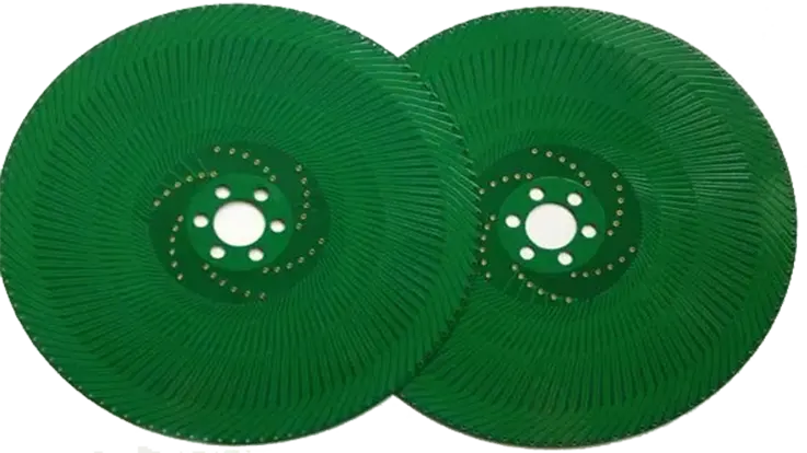
Designing LED PCBs involves navigating a variety of complex challenges. From managing heat dissipation to optimizing high-power LED circuits and controlling signal noise in tightly packed designs, each obstacle requires careful consideration and innovative solutions. In this section, we’ll explore some of the major hurdles designers face in LED PCB design and how these challenges can be effectively addressed.
Heat Dissipation and Thermal Expansion Issues
One of the most pressing challenges when designing LED PCBs is dealing with heat dissipation. LEDs generate a significant amount of heat during operation, and heat management is a critical factor in determining the longevity and performance of the PCB. If heat isn’t managed properly, it can lead to thermal expansion issues, damaging the LED components and potentially shortening their lifespan. In fact, poor thermal management is often one of the top reasons for LED failure in various applications.
To tackle this, designers typically incorporate specialized heat sinks or thermal vias into their LED PCB designs. Thermal vias help to conduct heat away from sensitive components, directing it toward the back of the PCB, where it can be dissipated more effectively. Additionally, the use of aluminum-based PCBs can also enhance heat dissipation. Aluminum, being a good conductor of heat, is often used in LED applications where high heat levels are a concern, such as automotive lighting or high-power commercial lighting.
Another innovative solution involves using graphene or nano-ceramic materials, which are excellent at conducting heat, allowing for more efficient cooling. These materials can be integrated into LED PCBs to maintain optimal temperatures, even in high-power configurations.
Here’s a breakdown of heat dissipation solutions and their effectiveness:
| Method | Description | Effectiveness |
| Thermal Vias | Channels within the PCB that allow heat to pass through | Highly effective for heat management |
| Heat Sinks | Metal fins attached to the PCB to dissipate heat | Essential for high-power applications |
| Aluminum Substrates | Using aluminum as the base material for better heat flow | Excellent for managing high thermal loads |
| Graphene/Nano-Ceramics | Advanced materials for enhanced thermal conductivity | Ideal for high-performance LEDs |
Efficient heat dissipation isn’t just about preventing component failure; it also ensures the reliability and performance of the LED PCBs, providing longevity and energy savings for end users.
High-Power LED Circuit Design
Designing circuits for high-power LEDs presents unique challenges compared to standard LEDs. These LEDs operate at much higher voltages and currents, requiring stronger circuit designs to ensure stable and reliable performance. High-power LEDs are commonly found in applications like automotive headlights, outdoor lighting, and medical devices, where high brightness and performance are required.
To handle the increased power demands, designers need to focus on current regulation and voltage stability. A common approach is to use constant current drivers, which maintain a stable flow of electricity to the LEDs, preventing fluctuations that can lead to damage. Additionally, power distribution in the LED PCB must be optimized to minimize resistance and prevent power loss, which could lead to excessive heat and reduced efficiency.
The key to effective high-power LED PCB design is to balance performance with heat management. Thermal management techniques, such as integrating heat sinks and using high-conductivity materials, work hand-in-hand with circuit design to maintain optimal performance.
Here’s a summary of key high-power LED circuit design elements:
| Design Element | Focus | Challenges |
| Constant Current Drivers | Ensures steady power supply to LEDs | Managing efficiency at high currents |
| Power Distribution | Optimizes current and voltage flow | Reducing power loss and heat buildup |
| Thermal Management | Controls heat generated by high-power LEDs | Preventing component damage from heat |
Designers must also pay attention to component layout and trace width to ensure current flow is managed effectively. With the right approach, high-power LED PCBs can deliver superior performance without compromising longevity.
Managing Signal Noise and EMI in Dense Designs
As LED PCBs become more complex, particularly in high-density designs, managing signal noise and electromagnetic interference (EMI) becomes increasingly difficult. Dense designs with multiple components and power-sensitive circuits are susceptible to EMI, which can distort signals, reduce efficiency, and lead to malfunctioning. This is particularly problematic in designs where precise signal integrity is a requirement, such as in communications equipment, medical devices, and consumer electronics.
One solution to combat EMI is to incorporate shielding into the PCB design, which can effectively block unwanted electromagnetic waves. Designers may also use ground planes to reduce EMI, providing a low-resistance path for current to flow and diverting electromagnetic fields away from sensitive components.
Furthermore, signal integrity can be improved through careful trace routing and component placement. Avoiding cross-talk between traces and ensuring that power and signal traces are routed separately can minimize noise interference. Additionally, the use of filtered power supplies can reduce the impact of noise on the overall performance of the LED PCB.
Here’s a quick comparison of common solutions to signal noise and EMI in LED PCB design:
| Solution | Description | Effectiveness |
| Shielding | Encasing sensitive components in conductive material | Highly effective in blocking EMI |
| Ground Planes | Creating a continuous ground connection across the PCB | Minimizes EMI and improves signal integrity |
| Trace Routing | Properly routing signal and power traces to reduce noise | Essential for noise reduction |
| Filtered Power Supplies | Using filters to clean the power input to the PCB | Effective at preventing noise from power supply |
When it comes to dense LED PCB designs, getting these factors right can be the difference between an efficient, stable design and one prone to malfunctions or poor performance.
Advanced Manufacturing Processes for LED PCBs
Manufacturing high-quality LED PCBs is no easy task. It involves a series of sophisticated processes that ensure the board performs optimally under challenging conditions. This section will dive into three major aspects of the manufacturing process: substrate preparation and selection, fabrication techniques, and testing and quality assurance. Each of these steps is crucial in delivering reliable and high-performance LED PCBs that stand the test of time.
Substrate Preparation and Selection
The substrate of any LED PCB is its backbone, providing essential support for both thermal management and mechanical stability. Choosing the correct substrate material is crucial to ensure efficient heat dissipation and that the board can handle the electrical load without degrading over time. This choice directly impacts the longevity and reliability of the LED PCB, ensuring that it can perform consistently under demanding conditions. With the right substrate, your LED PCB will not only last longer but also maintain optimal performance for a variety of applications.
The most common substrates used for LED PCBs include:
●Aluminum: Aluminum is a top choice for high-power LED applications thanks to its excellent ability to dissipate heat and its long-lasting durability. This material is commonly used in lighting systems where managing heat is a major concern. Its thermal properties make it ideal for environments where high performance is needed, ensuring that heat doesn’t build up and affect the LED’s efficiency. If you’re looking for a material that can stand the test of time while keeping things cool, aluminum is where it’s at—trusted for both its durability and its heat-busting capabilities.
●Ceramic: A premium material used for high-performance applications. Ceramics offer outstanding thermal conductivity and are suitable for use in industrial machinery or medical devices where heat resistance is needed.
●Flexible substrates: For applications requiring bendable boards, flexible PCBs are becoming more popular. Flexible substrates allow for more versatile designs, especially in wearable electronics and consumer gadgets.
The selection of the substrate depends on various factors, including the power requirements, operating environment, and thermal management needs. For instance, aluminum-based LED PCBs are commonly found in automotive lighting, while ceramic substrates are often used in high-end lighting systems or advanced medical equipment.
| Substrate Material | Thermal Conductivity | Best Use Cases |
| Aluminum | Excellent (100-220 W/mK) | Automotive lighting, streetlights, industrial applications |
| Ceramic | Outstanding (200-300 W/mK) | High-performance devices, medical equipment, industrial systems |
| Flexible Substrates | Moderate to Good (50-100 W/mK) | Wearables, consumer electronics, portable devices |
By carefully choosing the right substrate material, manufacturers can ensure that the LED PCB is durable, performs efficiently, and has a long lifespan. Don’t skimp on this step—it’s your board’s backbone!
Fabrication Techniques for LED PCBs
The fabrication of LED PCBs is where the magic happens. From the moment the substrate is selected, a series of processes begin to take shape. The goal is to create a board that’s efficient, cost-effective, and most importantly, capable of delivering the desired performance.
Here are the major fabrication techniques used in LED PCB manufacturing:
1.Printed Circuit Board Etching: This involves creating the necessary traces on the board. Etching removes unwanted copper, leaving behind the paths where electrical currents will flow. This step must be precise, as any imperfections can disrupt the signal integrity and electrical performance.
2.Drilling: For through-hole LEDs or thermal vias, the PCB must be drilled to allow for electrical connections between layers. Drilling must be done with extreme precision to avoid damaging the substrate or creating short circuits.
3.Surface Mount Technology (SMT): This technique places SMD LEDs onto the PCB with high accuracy, enabling automated assembly. The method ensures precise LED placement, making it particularly well-suited for applications with tightly packed circuits. Automated processes make it possible to scale up production efficiently, while maintaining consistent quality. In designs where space is limited, this approach ensures that everything fits exactly where it needs to be, allowing high-density configurations to function as expected, without any hassle.
4.Lamination: For multi-layer PCBs, lamination is used to bond the layers together. This process ensures that each layer is securely affixed, and that the electrical paths between the layers are consistent.
| Fabrication Step | Purpose | Key Considerations |
| PCB Etching | Creates electrical traces on the PCB | Requires precision to avoid electrical failure and heat buildup |
| Drilling | Makes holes for through-hole components and vias | Must be accurate to avoid short circuits or damage to the board |
| SMT Assembly | Places SMD LEDs onto the board for automated production | Ensures efficient production and consistent placement of LEDs |
| Lamination | Bonds multiple PCB layers together | Vital for multi-layer PCBs used in complex devices |
When all these steps come together, you’ve got a fully functional, high-quality LED PCB that’s ready to do its job. But don’t relax just yet—there’s one more stage to ensure the board will perform without issue: testing and quality assurance.
Testing and Quality Assurance
In the world of LED PCBs, testing is more than just a final step—it’s a non-negotiable part of the manufacturing process. Testing ensures that the LED PCB meets the required performance standards and that there are no hidden flaws that could lead to malfunction or failure. The goal is to catch potential problems before the product reaches the consumer.
There are several key tests conducted during and after PCB fabrication:
1.Visual Inspection: The first line of defense in quality control is a thorough visual inspection. This involves checking for defects such as scratches, scrapes, or misalignment of components.
2.Electrical Testing: Continuity testing and in-circuit testing (ICT) are performed to ensure that all electrical paths are functioning correctly and that there are no shorts or open circuits.
3.Thermal Testing: Thermal testing is key to verifying that heat management strategies are working as expected during normal operation. This testing evaluates how well the LED PCB dissipates heat, ensuring that components remain at safe temperatures even under load. Without proper heat control, the performance of an LED circuit could degrade or lead to failure. Thermal testing simulates real-world conditions, confirming that heat is efficiently transferred away from sensitive components, preserving their longevity and preventing any issues down the line. It’s like giving your LED design a “stress test” to make sure it holds up when the heat is on.
4.Life Cycle Testing: This tests the longevity of the PCB by simulating long-term usage in real-world conditions, such as extreme temperatures, humidity, and electrical stress.
| Test Type | Purpose | Best Use Cases |
| Visual Inspection | Identifies defects or misalignments in components | Initial testing to catch manufacturing flaws |
| Electrical Testing | Ensures all electrical connections are functional | Prevents short circuits or open circuits from causing issues |
| Thermal Testing | Verifies heat dissipation and thermal efficiency | Ensures the PCB doesn’t overheat, affecting LED performance |
| Life Cycle Testing | Simulates long-term use to check for durability | High-performance LED applications like street lighting or industrial equipment |
Assembly and Soldering Techniques for LED PCBs
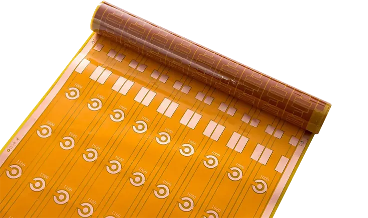
When it comes to LED PCBs, the assembly and soldering process is where the magic really happens. Whether you’re assembling a complex multi-layer PCB or something simpler, mastering the techniques involved is key to ensuring your LED PCBs perform at their peak. In this section, we will explore Surface Mount Technology (SMT) for LED assembly, the common pitfalls in soldering defects, and the best inspection methods to ensure your LED PCB assembly is flawless.
Surface Mount Technology (SMT) for LED Assembly
Surface Mount Technology (SMT) has revolutionized the way we assemble LED PCBs, especially for high-volume production. With SMT, components are mounted directly onto the surface of the PCB, eliminating the need for holes and making the process faster and more efficient. This technology is particularly effective for SMD LEDs, which are widely used in lighting systems, consumer electronics, and displays.
The SMT process involves several stages:
1.Solder Paste Application: A thin layer of solder paste is applied to the PCB’s pads where components will be placed. This paste contains tiny beads of solder and flux, and it helps in the electrical and mechanical connection of components to the PCB.
2.Component Placement: Using machines like pick-and-place robots, the components (e.g., SMD LEDs) are precisely placed onto the PCB.
3.Reflow Soldering: The board is then passed through a reflow oven, where the solder paste melts and forms a secure bond between the PCB and the components.
SMT is a great choice for high-density PCBs as it allows for the placement of many small components on a single board without compromising performance. This is especially useful when creating slim profile designs, such as in wearables and portable electronics.
| Step | Description | Advantages |
| Solder Paste Application | A thin layer of paste is applied to PCB pads | Ensures precise placement and strong electrical connections |
| Component Placement | Automated machine places SMD components onto the board | Increases speed, reduces human error, and ensures accuracy |
| Reflow Soldering | The board passes through a heated oven to melt solder paste | Forms reliable, high-quality solder joints |
By utilizing SMT, we can achieve faster production times, better component placement accuracy, and a more compact assembly. If you’re looking to accelerate production and enhance reliability, SMT is the way to go.
Avoiding Common Soldering Defects
Soldering defects can be a huge headache, not just for the manufacturer but for the end user too. Whether it’s a cold solder joint, bridging, or poor wetting, these issues can compromise the performance of your LED PCBs and lead to costly repairs or replacements. Let’s explore some of the most common soldering defects in LED PCB assembly and how to avoid them.
1.Cold Solder Joints: These occur when the solder doesn’t melt properly, leaving a weak connection between the component and the PCB. Cold joints can cause intermittent connections and signal loss, affecting the LED’s functionality.
●Prevention: Ensure that the soldering iron temperature is set correctly (around 350°F or 180°C for lead-free solder) and that the joint is heated uniformly.
3.Solder Bridging: This happens when excess solder forms a bridge between two adjacent pins, potentially shorting them. This is a particularly common issue when working with high-density SMT components.
●Prevention: Use precise soldering techniques and ensure that the soldering iron’s tip is clean and well-maintained to avoid over-application of solder.
3.Poor Wetting: When the solder doesn’t properly adhere to the pads or components, it results in a weak connection. This is especially problematic with lead-free solder, which requires higher temperatures.
●Prevention: Ensure proper flux application and use high-quality solder with the appropriate melting point for your board’s components.
4.Tombstoning: This defect occurs when one side of an SMT component lifts off the PCB due to uneven heating or an incorrect solder amount.
●Prevention: Use precision placement equipment and carefully monitor the reflow soldering process.
By keeping an eye on these common soldering defects and implementing the right techniques, you can improve the reliability of your LED PCBs and reduce the chances of early failure. Remember, a clean PCB and accurate soldering go hand in hand for a long-lasting product!
| Defect | Description | Prevention Tips |
| Cold Solder Joint | A weak solder connection due to insufficient heating | Ensure correct soldering iron temperature and uniform heat |
| Solder Bridging | Excess solder forms a bridge between pins, causing short circuits | Use precise soldering techniques and clean soldering tips |
| Poor Wetting | Solder doesn’t adhere properly to the pads | Apply sufficient flux and use quality solder with the correct melting point |
| Tombstoning | One side of the component lifts off the PCB | Use accurate component placement and monitor the reflow process |
By eliminating these soldering defects, you can guarantee that your LED PCBs will have reliable electrical connections, consistent performance, and long-term durability.
Inspection Methods for Assembled LED PCBs
Once the soldering process is complete, it’s time to inspect the assembled LED PCBs to ensure that everything is up to par. Without proper inspection, you might miss out on subtle defects that could lead to failures down the line. Let’s take a look at some of the top inspection methods used in LED PCB assembly.
1.Visual Inspection: This is the first line of defense. Skilled operators visually check for any obvious defects, such as misaligned components, incorrectly soldered joints, or damaged pads.
●Tip: Use magnification tools or automated optical inspection (AOI) systems for more precise visual inspections.
2.Automated Optical Inspection (AOI): AOI machines use high-resolution cameras and sophisticated software to scan the board for issues such as misplaced components, solder defects, and dimensional errors. This technology is particularly useful in high-volume production where manual inspection would be time-consuming.
●Tip: Ensure that the AOI system is properly calibrated for LED PCBs, as some SMD components can be challenging to inspect due to their small size.
3.X-Ray Inspection: For multi-layer PCBs, X-ray inspection helps in identifying internal soldering issues like voids, bridging, or insufficient solder between layers. It provides a non-invasive way to inspect the inner workings of the PCB, making it a must-have for high-end applications.
●Tip: Use X-ray inspection for more complex LED PCBs that have components buried within the layers.
4.Functional Testing: In this stage, the board is powered up, and LED performance is tested. This ensures that each LED on the board is working and that no electrical issues are present.
●Tip: Run stress tests under varying temperatures and voltages to simulate real-world conditions and ensure that the board performs well over time.
| Inspection Method | Purpose | Best Use Cases |
| Visual Inspection | Detects visible defects such as misalignments or damaged pads | Entry-level inspection for basic quality control |
| Automated Optical Inspection (AOI) | Scans the board for defects like misplacement or solder issues | High-volume production and complex designs |
| X-Ray Inspection | Identifies issues like voids or bridging within multi-layer PCBs | Complex, multi-layer LED PCBs needing internal inspection |
| Functional Testing | Verifies LED operation and electrical functionality | Ensures the final product works under real-world conditions |
By utilizing these inspection methods, we can guarantee that the final LED PCB assembly meets all the necessary quality standards and is ready to perform as expected. Whether you’re using manual inspection, AOI, or X-ray, always double-check your work—it’s the best way to ensure quality control.
Innovations in LED PCB Materials and Technologies
As technology continues to evolve, LED PCBs are becoming more sophisticated, pushing boundaries in design, efficiency, and sustainability. From emerging substrates to eco-friendly manufacturing practices and smart lighting integration, the industry is exploring groundbreaking innovations that promise to enhance the performance and longevity of LED PCBs while meeting the growing demand for sustainable and intelligent solutions. In this section, we’ll dive into these cutting-edge advancements and explain how they are reshaping the future of LED PCB technologies.
Emerging Substrates: Graphene and Nano-Ceramics
The quest for better-performing LED PCBs has led to a rise in the use of novel substrates, with graphene and nano-ceramics making waves in the industry. These materials offer exceptional thermal conductivity, electrical performance, and mechanical strength, making them ideal for high-performance LED applications.
Graphene, a single layer of carbon atoms arranged in a two-dimensional lattice, has been hailed as a game-changer in various fields, and its application in LED PCBs is no exception. Known for its excellent thermal dissipation properties, graphene can help manage the heat generated by LEDs, improving efficiency and lifespan. When paired with traditional copper or aluminum substrates, graphene enhances the thermal management of LED PCBs, making it a preferred choice for high-power applications like automotive lighting and industrial equipment.
Similarly, nano-ceramics are emerging as another innovative material for LED PCB substrates. These materials are lightweight, durable, and highly resistant to heat, offering superior thermal conductivity compared to standard ceramics. As nano-ceramics become more widely available, they’re expected to offer cost-effective solutions for high-end LED designs, particularly in consumer electronics and lighting products.
Here’s a quick comparison of graphene and nano-ceramics in terms of key properties:
| Property | Graphene | Nano-Ceramics |
| Thermal Conductivity | Exceptional (high) | High, but slightly lower than graphene |
| Electrical Conductivity | High | Moderate to high |
| Durability | Strong and flexible | Very strong, highly resistant to wear |
| Cost | High due to limited availability | Moderate, more cost-effective |
Eco-Friendly Manufacturing Practices
With sustainability at the forefront of manufacturing today, eco-friendly practices are becoming a must in the LED PCB industry. Manufacturers are increasingly adopting green technologies to reduce the environmental footprint of their production processes. This includes the use of lead-free soldering, recyclable materials, and reducing waste during the manufacturing stages.
Lead-free soldering has been a long-standing trend in the electronics industry, and it is now the standard for LED PCB assembly. This method eliminates harmful substances from the production process, making LED PCBs more environmentally friendly. RoHS-compliant components are becoming more common, and manufacturers are encouraged to move towards eco-friendly chemicals that are less toxic and more biodegradable.
Additionally, the rise of recyclable PCB materials, like biodegradable laminates and environmentally friendly solder masks, is giving manufacturers new ways to design LED PCBs that meet green standards. More companies are also investing in closed-loop manufacturing systems to recycle scrap materials and reduce overall waste. This results in a more sustainable product lifecycle for LED PCBs, from initial production to end-of-life recycling.
Here’s a simple breakdown of eco-friendly manufacturing practices for LED PCBs:
| Practice | Impact |
| Lead-free Soldering | Reduces hazardous waste and toxins |
| Recyclable Materials | Minimizes waste and supports circular economy |
| Eco-friendly Solder Masks | Uses biodegradable or non-toxic materials |
| Closed-Loop Systems | Reduces production waste and recycles materials |
These advancements not only help to reduce the environmental impact but also align with global efforts to promote sustainability and eco-conscious manufacturing in the electronics industry.
Smart Lighting Integration with LED PCBs
The integration of smart lighting systems with LED PCBs is one of the most exciting developments in the industry. The Internet of Things (IoT) is bringing LED PCBs to life in ways we’ve never seen before, making lighting systems more efficient and intelligent.
With the rise of smart cities, smart homes, and connected devices, LED PCBs are evolving to meet the needs of modern lighting systems. These smart LEDs allow users to control and customize their lighting environment in real-time through smartphones, voice assistants, or automated systems. For instance, smart lighting systems embedded with LED PCBs can adjust brightness, color temperature, and even sync with motion sensors to save energy and create a more personalized experience.
The integration of sensors like ambient light sensors, motion detectors, and occupancy sensors directly into LED PCBs is enabling intelligent lighting solutions that can adapt to changing environments. This innovation allows for energy savings, improved user experience, and extended product lifecycles.
Here’s a simple look at how smart lighting integration is changing the way we use LED PCBs:
| Feature | Benefit |
| Smartphone Control | Allows for remote control and customization of lighting |
| Motion Sensors | Reduces energy consumption by automatically adjusting lighting when needed |
| Ambient Light Sensors | Adjusts light intensity based on the surrounding environment |
| Voice Assistant Integration | Provides hands-free control for lighting systems |
Why Choose Us for Your LED PCBs Project?
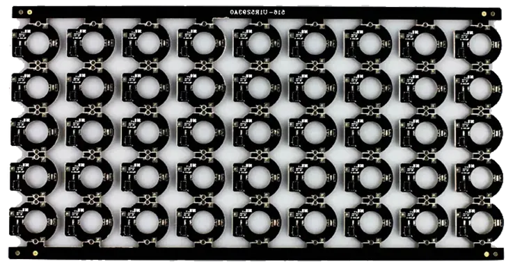
1.Professional LED PCB Board Manufacturer – JarnisTech
At JarnisTech, we pride ourselves on being a trusted manufacturer of high-quality LED PCBs. With over two decades of experience, we offer comprehensive services, including LED PCB fabrication, component sourcing, and full PCB assembly. Our goal is to provide affordable LED PCBs tailored to your specific needs, no matter how complex your project may be. Whether you’re developing a high-power LED system or a specialized low-power lighting solution, we have the tools and expertise to deliver outstanding results.
2.Custom LED PCBs to Match Your Project Needs
We understand that each project is unique, and that’s why we offer customized solutions based on your Gerber files and Bill of Materials (BOM). Once you send us your customized files, our team will conduct a thorough review and provide you with a detailed quote. After that, it’s up to you to decide whether or not to move forward with the project. You can also choose to supply the parts for assembly, giving you complete control over the process.
We’re committed to meeting your needs with top-notch quality and competitive pricing, regardless of the LED application. Whether you’re a LED lamp manufacturer or working with outdoor LED screens, we’ll work closely with you to find the perfect solution for your unique requirements.
3.Comprehensive Product Offering
JarnisTech manufactures a wide range of LED PCBs to serve different applications and industries:
●High-Power LED PCBs: We specialize in high-performance aluminum base PCBs, copper base PCBs, and ceramic base PCBs, each designed to handle high power demands while maintaining efficient thermal management.
●Low-Power LED PCBs: For energy-efficient designs, we offer FR4 PCBs and high-temperature PCBs that are ideal for low-power LED solutions.
4.Innovating for a Brighter Future
At JarnisTech, we don’t just manufacture LED PCBs—we innovate. We are heavily involved in research and development, especially in the areas of heat conduction and LED lumen optimization. Our team is constantly exploring new methods to improve the performance and efficiency of LEDs. We understand that thermal management is one of the biggest challenges in LED design, which is why we focus on incorporating the latest thermal materials and advanced cooling solutions into our designs.
Moreover, while we do not sell LED lamps, we stand firm in our support of the LED industry. We collaborate with LED lamp manufacturers to ensure that they have access to the most reliable, durable, and efficient LED PCBs in the market.
Why Choose JarnisTech for Your LED PCB Needs?
| Feature | Benefit | Why Choose Us? |
| Decades of Experience | Over 20 years of expertise in LED PCB manufacturing | We understand the intricacies of PCB design and assembly. |
| Custom Solutions | Tailored LED PCBs based on your Gerber file and BOM | We make it easy to bring your unique project to life. |
| Comprehensive Services | From PCB fabrication to full assembly and component sourcing | We’re your one-stop-shop for all things LED PCB. |
| Innovative R&D | Cutting-edge research into thermal management and lumen efficiency | We push the boundaries of what’s possible in LED design. |
| Affordable Pricing | Competitive pricing without compromising on quality | We provide the best value for your investment. |
Let’s Get Started Today!
If you’re looking for a reliable, professional partner to support your LED PCB needs, JarnisTech is the way to go. Whether you’re developing high-power lighting systems, outdoor displays, or specialized low-power LEDs, we’ve got you covered.
Don’t hesitate to reach out today to discuss your project and get a customized quote. Our team is ready to help you bring your LED ideas to life—let’s create something amazing together!
FAQs related to LED PCBs
What is an LED PCB?
An LED PCB is a type of printed circuit board designed specifically to support and power LED (light-emitting diode) components.
What are the benefits of using LED PCBs?
LED PCBs offer better heat dissipation, durability, and improved lighting efficiency compared to traditional light sources.
What are common types of LED PCBs?
Common types include aluminum-based, flexible, and ceramic-based LED PCBs, each suited for different applications and environments.
Why is thermal management important in LED PCB design?
Effective thermal management ensures that LEDs operate at optimal temperatures, extending their lifespan and improving performance.
Can LED PCBs be customized?
Yes, LED PCBs can be customized based on specific power, size, and application requirements, such as for high-power or outdoor LED lighting.
How are LED PCBs assembled?
LED PCBs are typically assembled using Surface Mount Technology (SMT), which involves placing LED components directly onto the board.
What industries use LED PCBs?
LED PCBs are used in a wide range of industries including automotive, consumer electronics, medical devices, and outdoor signage.
How do I choose the right LED PCB for my project?
Consider factors like heat dissipation, power requirements, flexibility, and environmental conditions when selecting an LED PCB for your application.


