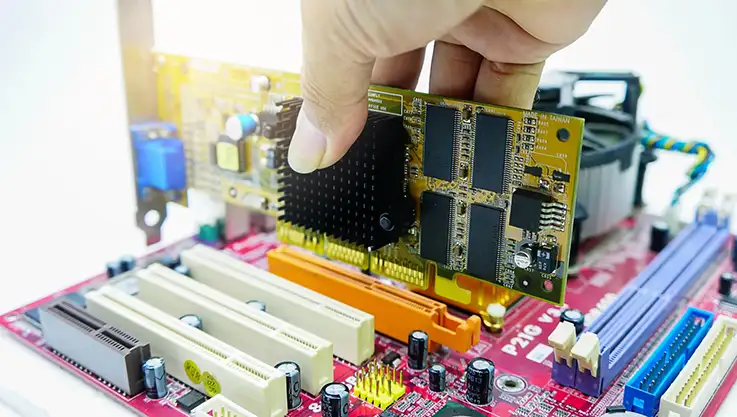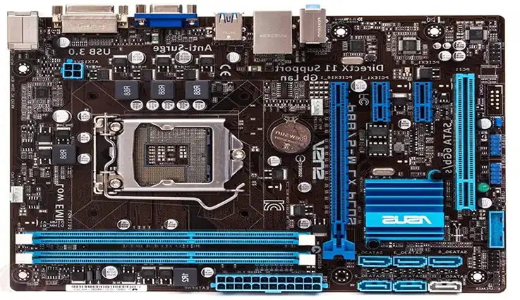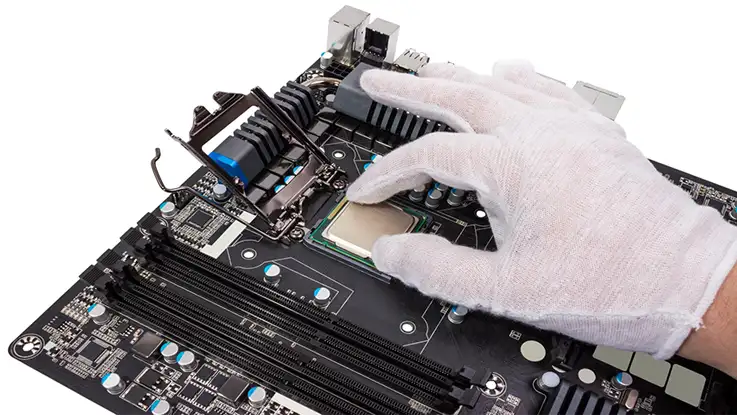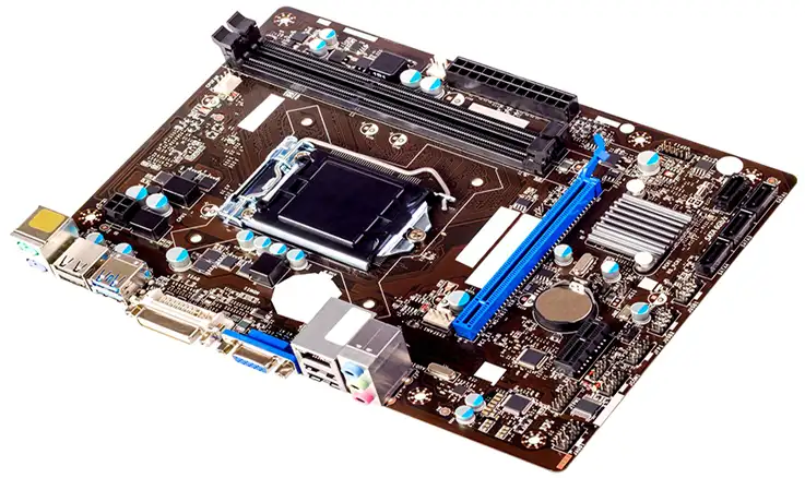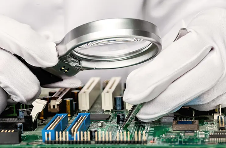
In the world of electronics, the computer PCB (Printed Circuit Board) is a foundational element that drives the performance, efficiency, and reliability of modern computing systems. As computers continue to evolve, so do the demands placed on computer PCB design and manufacturing. In this guide, we will explore the intricate process of designing, manufacturing, and assembling computer PCBs—from the initial design phase to the final assembly, all while addressing the key considerations for quality control, materials selection, and sustainability.
Essential Elements of Computer PCB Design
Designing a computer PCB isn’t just about sketching out a blueprint for connecting electrical components—it’s about building a robust platform capable of handling a multitude of computing tasks. From ensuring that the system can process high data volumes efficiently in multi-layer PCBs to minimizing interference in high-speed applications, the design process is key to creating a high-performance, reliable circuit board. Think of it like a roadmap: the clearer and more efficient the layout, the better the journey (or in this case, the performance) of your computer. Now, let’s take a deeper dive into what goes into the computer PCB design process.
Types of Computer PCBs and Their Applications
When you’re crafting a computer PCB, picking the right type is the first move. It’s like selecting the right tool for the job—it’s about ensuring your design is fit for the task at hand.
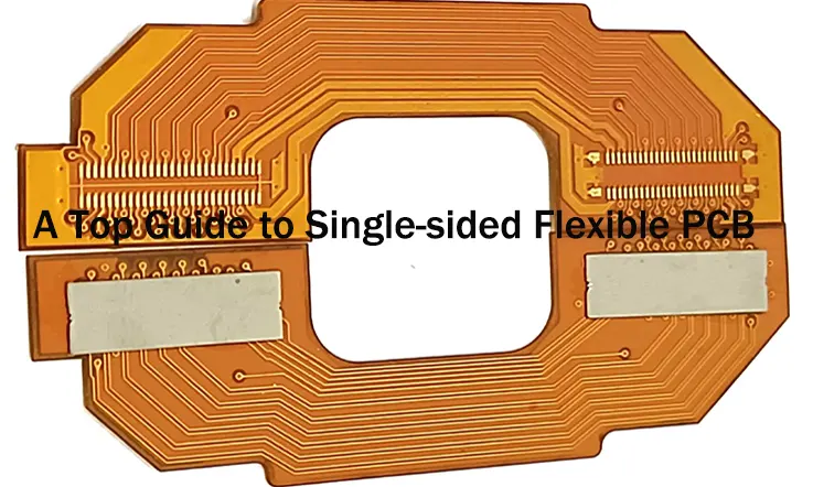
1.Single-layer PCBs: These are often the choice for less complex systems. Their simpler design means they’re easier to produce, less expensive, and ideal for basic electronics. But don’t let their simplicity fool you—single-layer PCBs can still pack a punch in basic computing applications like calculators or small, consumer-grade electronics.
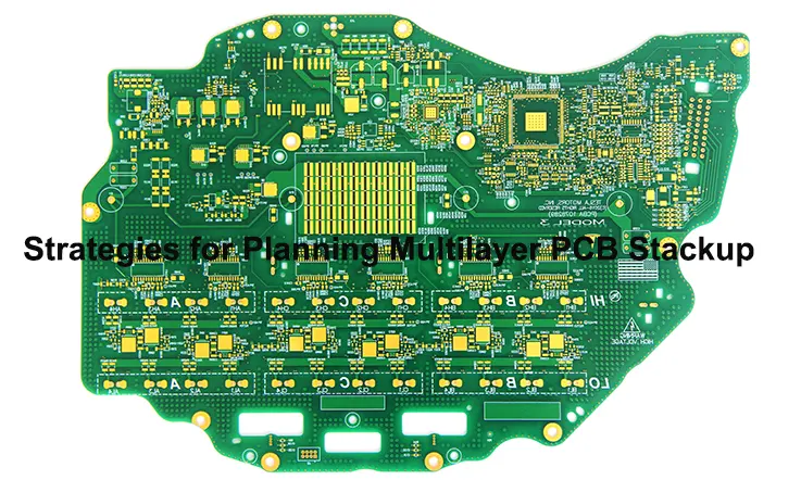
2.Multi-layer PCBs: Now, when you’re dealing with more complex systems like personal computers, servers, or gaming devices, multi-layer PCBs are your best bet. These designs stack multiple layers of copper circuitry with insulating materials in between, allowing for higher circuit density. As a result, multi-layer PCBs can handle more complex signal routing and support more components without increasing the size of the board.
3.High-frequency PCBs: If you’re diving into high-speed data processing, this is where high-frequency PCBs shine. These are optimized to handle faster signal transmission with minimal signal degradation—think of gaming PCs or high-performance servers that need lightning-fast processing speeds.
Below is a comparison table of different PCB types:
| PCB Type | Key Components | Application | Example Usage |
| Single-layer PCB | Resistors, Capacitors, Diodes | Basic devices, low-complexity systems | Basic electronics, calculators |
| Multi-layer PCB | Transistors, Capacitors, ICs | Complex systems, higher data density | Personal computers, servers, gaming PCs |
| High-frequency PCB | Specialized RF Components | High-speed signal transmission | High-performance servers, gaming systems |
When choosing a PCB type, each option comes with unique strengths and trade-offs, and selecting the right one can directly impact how well your product functions. Whether you’re working with single-layer, multi-layer, or flexible PCBs, understanding what each type brings to the table is essential. The right choice enhances performance and efficiency, while a less optimal match could slow things down. Choosing wisely here means fewer headaches down the road and keeps your project humming along like a well-oiled machine.
Core Components in Computer PCB Layout
Each computer PCB is powered by essential components—transistors, resistors, capacitors, and more—all carefully chosen and positioned to drive the board’s function. These parts aren’t just extras; they’re what bring the board to life. Proper placement and layout of each component ensure efficient signal flow and power distribution, keeping everything on track. Think of it as the heart and soul of the circuit; when each piece is in the right spot, this layout ensures that signals pass through cleanly, making the whole system reliable and efficient for whatever tasks it’s built to handle.
1.Transistors: These little electronic switches are used to control the flow of electrical current. In computer PCBs, transistors are placed in positions where they can regulate power across the board. Think of them as traffic cops directing the flow of electricity where it’s needed most.
2.Capacitors: These store electrical energy and release it when necessary. This function is especially valuable in processors and other high-demand parts, where consistent energy supply is a must to avoid fluctuations that could impact performance. By smoothing out power delivery, they keep everything on an even keel, especially in setups that push the limits, like high-performance computing applications.
3.Resistors: Resistors are the speed bumps of the electrical flow. They manage current and prevent components from getting overloaded. Strategically placing resistors can help avoid overloading circuits and ensure steady, reliable operation.
When these components are properly laid out, the computer PCB can maintain smooth performance. A well-designed board ensures that electrical signals flow where they’re supposed to, with minimal interference, and with proper energy management.
Key Principles in Computer PCB Circuit Design
In any computer PCB design, the aim is to keep electrical signals flowing cleanly and efficiently. Here are some of the core principles that guide designers in achieving this:
1.Trace Width and Routing: Think of trace width as the size of the electrical “highways” on your board. The wider the trace, the more power it can carry. It’s like deciding how wide a road should be to handle traffic. Getting this right ensures that your signals can flow smoothly without overheating or losing power.
2.Signal Integrity: This is all about making sure that the electrical signals on your computer PCB don’t get distorted. Just like a bad phone line can make it hard to hear someone clearly, poor signal integrity leads to corrupted data. Using good signal routing practices and minimizing crosstalk between lines is a must.
3.Impedance Matching: Impedance is the resistance a signal encounters as it travels through a circuit. If you don’t match the impedance properly in your PCB design, the signals can reflect back and cause errors. It’s like when you’re driving and hit a speed bump—your signal is reflected back instead of moving forward, which can cause system failures.
Here are some of the core principles that guide designers in achieving this:
| Design Factor | Impact on Signal Integrity | Recommended Solution |
| Trace Width | Determines current capacity and heat dissipation | Adjust width based on power requirements |
| Signal Routing | Ensures data travels cleanly, preventing noise | Keep traces short, use dedicated ground planes |
| Impedance Matching | Prevents signal reflection and loss | Use controlled impedance traces for high-speed circuits |
The goal in PCBs is to achieve a balanced design where all components interact smoothly with each other. For designers, this requires constant attention to detail and a deep understanding of how electrical signals behave in the system.
Advanced Computer PCB Manufacturing Processes
The manufacturing process of computer PCBs demands high precision and attention to detail. Achieving the optimal balance between design, cost-efficiency, and functionality requires advanced techniques in assembly, quality assurance, and production methods. Let’s explore how the latest PCB manufacturing technologies are applied to computer systems.
Surface Mount Technology (SMT) in Computer PCBs
Surface Mount Technology (SMT) has revolutionized the way components are placed onto PCBs. In this process, electronic components are directly mounted onto the surface of the PCB, eliminating the need for through-holes that were common in older designs. The key advantage here? SMT allows for higher component density, which means faster, more powerful PCs.
Process Breakdown:
1.Component Placement: Small components like resistors, capacitors, and microchips are positioned on the PCB with extreme accuracy.
2.Soldering: After the components are placed, they are soldered onto the board using a process called reflow soldering. This method uses heat to melt solder paste, creating secure connections.
3.Inspection: Automated optical inspection (AOI) machines check for misplaced components or soldering issues, ensuring that the PCB meets the required standards.
| Advantage | Description |
| High Component Density | SMT allows for more components to be placed on the board, enabling faster and more compact designs. |
| Automated Process | Reduces the risk of human error, improving consistency and production speed. |
| Smaller Footprint | Components are much smaller compared to traditional methods, saving space and weight. |
While SMT brings numerous benefits, it also presents challenges such as the fragility of small components and the need for precise alignment during assembly. But with today’s advanced equipment, these challenges can be addressed effectively, resulting in reliable and efficient computer PCBs.
Utilizing Dual Inline Package (DIP) Techniques
Dual Inline Package (DIP) components are a reliable go-to in PCB assembly, especially for applications that prioritize durability and straightforward implementation. Although Surface Mount Technology (SMT) dominates today’s designs due to its compact profile and efficiency, DIP retains popularity for components that benefit from stronger mechanical connections. This makes it a natural fit for cases where long-term stability is a must and ease of repair or replacement is appreciated. DIP assemblies stand their ground, keeping things functional without the extra frills.
DIP Process Overview:
1.Component Insertion: Components with two rows of pins are inserted through holes in the PCB, which are then soldered on both sides.
2.Manual or Wave Soldering: Depending on the size of the batch, wave soldering may be used, where a flow of molten solder is passed over the board, automatically soldering all components at once.
3.Testing: Post-soldering, each DIP component is thoroughly tested for electrical continuity and quality assurance.
| Advantages of DIP | Use Case |
| Sturdiness | DIP components are robust and provide strong electrical connections. |
| Ideal for Prototyping | Great for testing circuits before mass production, thanks to easy component removal. |
| Cost-Effective | For lower-volume products, DIP assembly is often less expensive. |
Despite the rise of SMT, DIP remains ideal for low-volume runs and specialized equipment. For computers, DIP is often used for components like microcontrollers and ICs that require a more durable connection.
Quality Control and Testing for Computer PCB Manufacturing
A computer PCB is only as good as the testing it undergoes during manufacturing. Ensuring high performance and longevity requires a comprehensive approach to quality control. The testing process can involve multiple methods to ensure the PCB meets the strict demands of computer systems.
Testing Techniques:
1.In-Circuit Testing (ICT): This checks each component of the PCB while the circuit is powered. It’s a fast and accurate way to identify faulty connections or defective components.
2.Automated Optical Inspection (AOI): This visual inspection method uses cameras to capture high-resolution images of the PCB, comparing them with a design file to ensure proper placement of components.
3.Functional Testing: After assembly, the PCB is powered up and tested in a real-world environment. This ensures that the board operates as intended within the final system.
| Quality Control Method | Purpose | Benefit |
| In-Circuit Testing (ICT) | Detects faults in the individual components. | Quick and accurate detection of defects. |
| Automated Optical Inspection | Ensures proper component placement and soldering. | Minimizes the chance of human error. |
| Functional Testing | Validates the PCB’s overall functionality. | Ensures the board performs under real conditions. |
Automated optical inspection (AOI) is a key technology in upholding quality in PCB manufacturing. This method swiftly detects even the tiniest defects by analyzing each layer and component with pinpoint precision. By identifying issues such as misalignments, soldering problems, or missing parts, AOI minimizes the risk of costly errors when scaling to large production runs. This process not only saves time and resources but also ensures each board meets the high standards demanded by today’s advanced electronics industry—an invaluable step for delivering a top-notch final product.
Best Practices in Computer PCB Assembly
Assembling computer PCBs demands a sharp eye for technical detail and a full grasp of design principles. Beyond simply placing components, this process is about harmonizing design with functionality for a board that performs flawlessly. Mastering best practices in PCB assembly can lead to highly efficient and high-performing boards while keeping production costs in check. Now, we’re sharing methods to optimize assembly, so you can deliver top-notch boards ready for the demands of modern computer systems—let’s dig in and make it count!
Prototyping and Pre-Production Computer PCB Assembly
Before diving into full-scale production, prototyping is a crucial phase in the computer PCB assembly process. This is where designers and engineers test their design ideas and ensure that everything works as intended before going into mass production.
Prototyping Process:
1.Initial Design and Simulation: Prototyping often begins with a simulation of the computer PCB design to check for signal integrity, thermal distribution, and overall performance. Tools like PCB design software allow designers to virtually test the layout before creating the first physical prototype.
2.Building the Prototype: After simulation, a prototype PCB is created. This first version is assembled with components and tested for functionality, providing valuable insights into any potential issues or design flaws.
3.Iterative Testing and Adjustments: If issues arise during prototype testing, modifications are made to the design. Prototyping is an iterative process, often involving multiple cycles to get the design perfect.
| Step | Description |
| Initial Simulation | Virtual testing to identify potential issues before building the physical prototype. |
| Prototype Assembly | Building the first version of the PCB with components for real-world testing. |
| Iterative Improvements | Modifying the design after each round of testing to achieve the best performance. |
Prototyping is the real test drive for your PCB design. This phase lets you make final tweaks on elements like component layout and trace sizes before moving forward with full production. It’s the chance to catch any hiccups early and optimize the board’s performance and durability. Fine-tuning here can save time and costs down the road, ensuring the design is ready to meet the demands of larger scale manufacturing.
Assembly Techniques for Embedded and High-Speed Applications
When dealing with embedded systems or high-speed computing applications, the assembly process needs to be tailored for the unique demands of these types of PCBs.
Assembly Process for Embedded PCBs:
1.Component Selection: Embedded systems often use specialized components, such as embedded microcontrollers or FPGA chips. These need to be carefully selected based on their compatibility with the PCB design and the intended application.
2.Integrated Circuit (IC) Packaging: IC packaging is central to high-speed systems, with BGA (Ball Grid Array) and QFN (Quad Flat No-lead) packages standing out due to their compact footprint and effective high-frequency signal management. These types allow for minimal lead inductance and better thermal management, ideal for designs where space-saving and speed are top priorities. In particular, their sturdy design and ability to handle intricate, high-density layouts make them reliable options for stable, high-performance connections in advanced circuitry.
3.Thermal Management: In high-speed applications, managing heat is a big deal. Engineers rely on tools like heat sinks, vias, and thermal pads to keep things cool and avoid overheating. By efficiently redirecting heat away from sensitive components, these solutions ensure that the system runs smoothly, preventing any hiccups that could mess with performance. When you’re pushing high-speed tech to the limit, getting the thermal management right is like keeping the engine of a race car cool during a race—no overheating, no delays.
| Application | Key Components | Challenges |
| Embedded PCBs | Microcontrollers, FPGA, Flash Memory | Managing signal integrity in tight spaces. |
| High-Speed PCBs | BGA, QFN, Signal Processors | Ensuring low latency and high-frequency performance. |
High-speed applications require advanced assembly techniques, including precision placement of components and fine-tuned soldering processes to ensure optimal performance. If you’re designing PCBs for high-speed computing like servers or gaming PCs, these techniques ensure the board can handle the demands of modern, data-intensive systems.
Minimizing Assembly Defects in Computer PCBs
A major goal in computer PCB assembly is minimizing defects. Defective boards can cause poor performance, short lifespans, or outright failure of the computer system. Even minor flaws can result in system instability or complete failure. That’s why focusing on precision throughout the process is necessary. Think of it as tuning a fine instrument—attention to detail ensures smooth operation and maximizes the board’s potential. Following best practices and fine-tuning at each step prevents costly mistakes, guaranteeing a more reliable and high-performing end product. Every action, no matter how small, impacts the final result.
Common Assembly Defects:
1.Solder Bridges: When excess solder creates unintended connections between pads or traces, it can cause a short circuit. This is typically due to improper soldering or too much solder paste during the assembly process.
2.Misaligned Components: Components that are improperly aligned or placed can lead to faulty connections. This is often a result of poor component placement or inaccurate pick-and-place machines.
3.Cold Solder Joints: Inadequate heating during soldering can result in weak or intermittent connections, leading to system instability. This can be prevented with more careful inspection and reflow soldering techniques.
| Defect Type | Cause | Solution |
| Solder Bridges | Excess solder during placement or reflow soldering. | Use automated solder paste inspection to ensure correct paste amounts. |
| Misaligned Components | Improper placement of components during assembly. | Invest in advanced pick-and-place equipment with alignment checks. |
| Cold Solder Joints | Insufficient heat during soldering. | Ensure proper reflow temperature profiles and soldering processes. |
Preventing defects goes beyond just fixing problems as they arise. It’s about implementing processes like automated inspection (AOI) to catch issues before they reach the consumer. A well-executed assembly process ensures your computer PCBs work the way they should, with fewer repairs and greater product reliability.
High-Performance Design Techniques for Computer PCBs
Creating high-performance computer PCBs is an art as much as a science. It’s about pushing the limits of signal integrity, speed, and density, while also ensuring reliable functionality across a wide range of computing applications. Whether you’re designing for gaming systems, workstations, or servers, advanced design techniques allow for efficient, high-performance PCBs that meet demanding specifications.
Multi-Layer PCB Design for High-Functionality Computers
In the pursuit of high-performance computer PCBs, multi-layer designs are often the go-to solution. By stacking multiple conductive layers, designers can maximize space, increase component density, and reduce signal interference—critical when designing complex computing systems that handle a variety of tasks.
1.Layer Stack-Up for High-Performance: Multi-layer PCBs allow for a more compact, efficient layout by utilizing internal layers for power distribution and signal routing. The typical multi-layer stack consists of signal layers, ground planes, and power planes, with each layer designed to minimize cross-talk and interference between signals.
●Inner Layers for Power Distribution: These inner layers are key to maintaining a smooth power supply to the board’s components, especially in high-demand systems like servers and powerful computers. Without them, the power flow could become inconsistent, causing system instability. Their role is to ensure that all components get the power they need to operate without interruptions or slowdowns. By offering this level of reliability, the system can perform at its peak, handling tasks without a hitch, even under heavy loads.
●Signal Layers for High-Speed Applications: By carefully arranging these layers, designers ensure that signals are routed with minimal interference, allowing for faster data processing and reducing latency in real-time computing applications.
| Layer Type | Purpose | Key Benefit |
| Signal Layers | Carry electrical signals between components | High-speed data transfer, reduced crosstalk |
| Power Planes | Distribute power evenly across the board | Stable voltage delivery, reduced noise |
| Ground Planes | Provide a reference for signals and reduce noise | Improved signal integrity and reduced electromagnetic interference (EMI) |
By designing multi-layer PCBs, you’re creating a solid foundation that enhances the overall performance of the computer system while maintaining the flexibility needed to handle complex designs and diverse applications.
High-Frequency Computer PCB Design and Signal Integrity
For systems handling large amounts of data at high speeds, signal integrity becomes a make-or-break factor. In high-frequency PCBs, the design must focus on reducing signal loss and shielding against electromagnetic interference (EMI). Without proper attention to these details, signal degradation can occur, leading to glitches or failures. Designing with these factors in mind helps ensure smooth and efficient data processing, which is a game-changer for performance in advanced computing systems.
Design Considerations for High-Frequency PCBs:
●Impedance Control: To preserve the integrity of high-frequency signals, the impedance of the PCB traces must be carefully controlled. Controlled impedance routing helps avoid signal reflection and loss, which can lead to data errors.
●Trace Width and Spacing: Precision in trace width and spacing ensures proper impedance matching and reduces the likelihood of signal distortion, especially in high-speed data transfer.
●Via and Layer Transitions: Vias (the small copper-plated holes used to connect layers) can introduce parasitic inductance and capacitance that degrade signal quality. Careful design of via sizes and placements can minimize this effect.
| Consideration | Impact on Performance | Solution |
| Impedance Matching | Prevents signal reflections and data errors | Use controlled impedance designs and matching of trace width. |
| Trace Width and Spacing | Ensures signals pass with minimal loss | Precision in designing traces for high-speed signals. |
| Via Design | Minimizes inductance and capacitance effects | Use micro-vias and optimize via locations. |
Achieving signal integrity in high-frequency designs ensures that data flows with minimal latency, allowing systems like servers, data centers, and gaming rigs to run at top speed without hiccups.
SSD and CPU Optimization in Computer PCB Layout
When designing PCBs for high-performance computing, the focus is not only on efficient signal routing but also on optimizing component placement, especially for key elements like SSDs and CPUs.
1.Optimizing for SSDs: The solid-state drive (SSD) is a critical component in any high-performance computer system. These components rely on fast data transfer speeds and low latency, which demands a PCB design that supports these needs.
●Component Placement for SSDs: SSDs should be placed with minimal trace lengths to reduce latency. Additionally, power planes and ground planes should be designed to reduce electromagnetic interference (EMI) that can affect data integrity.
●Thermal Management for SSDs: SSDs produce a lot of heat when they’re running at full speed, and that can really mess with their performance if it’s not kept under control. To handle this, thermal pads or heat sinks are added to manage the temperature, especially in high-speed applications.This helps keep the SSD from overheating and ensures it works without any hiccups, even under load. The added cooling components are a straightforward solution to help maintain the system’s overall health and avoid slowdowns.
1.CPU Placement and Routing: The CPU acts as the core engine in any high-performance setup, where its placement on the PCB and the routing of the traces can significantly impact efficiency. Correct positioning minimizes signal delays, ensuring smooth and consistent operation. Thoughtful trace design aids in maintaining a steady clock speed, allowing the system to handle intense workloads without hiccups. It’s about getting all the fine details right so the whole system performs at its peak, without a hitch.
●Short and Direct Routing: Keep traces to the CPU as short and direct as possible to reduce latency. Additionally, clock traces should be routed with care to maintain timing integrity.
●Thermal Design for CPUs: CPUs tend to heat up quickly under load, so careful thermal management is necessary. Heat sinks, thermal vias, and copper pours are commonly used to ensure heat is dissipated efficiently.
| Component | Design Focus | Benefit |
| SSD | Shorter trace lengths, proper placement, thermal management | Faster data transfer, reduced latency |
| CPU | Optimized trace routing, thermal design | Better performance, reduced heat buildup |
In the case of high-performance systems, the careful placement and design optimization of components like SSDs and CPUs ensures that the entire system performs at its peak, even under heavy loads.
Material Selection in Computer PCB Manufacturing
The material selection for computer PCBs is the backbone of every design. The performance, longevity, and overall functionality of a printed circuit board (PCB) rely heavily on the choice of materials. Designers and manufacturers must carefully select materials that align with the specific requirements of the system, such as durability, thermal resistance, and conductivity. The process is not just about choosing what’s available—it’s about selecting the best options for high-performance and high-reliability systems.
Choosing Substrates for Durable Computer PCBs
When it comes to substrates, which serve as the foundational layer for the PCB, the choice is based on several factors such as strength, durability, and cost-effectiveness. Substrates act as the body of the PCB, providing structural support and insulation. Epoxy fiberglass (FR4) is the most commonly used substrate for general-purpose PCBs due to its combination of strength and cost-effectiveness. However, more specialized systems may require high-performance materials to support advanced applications.
Common Substrates for Different Applications:
●FR4 (Epoxy Glass Fiber): The go-to choice for most computer PCBs, known for its durability and relatively low cost.
●Polyimide (PI): For high-performance flexible PCBs that require superior heat resistance and flexibility.
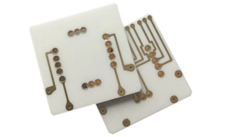
●Ceramic Substrates: Used in high-frequency and high-temperature environments, such as military, aerospace, and high-end computing applications.
| Substrate Type | Best Use | Benefits |
| FR4 | General-purpose, low-cost designs | Cost-effective, strong, and reliable |
| Polyimide (PI) | Flexible, high-performance systems | High thermal stability, flexible design |
| Ceramic | High-frequency, aerospace, military | Excellent heat resistance and low loss |
In the world of high-performance computing, the material choice directly affects the reliability and efficiency of the entire PCB. Choose wisely to ensure the board can withstand the environmental and operational demands of advanced systems.
Conductive Materials in High-Performance Computer PCBs
Conductive materials are at the heart of every PCB, as they form the pathways for electrical signals to travel through the board. Copper is the most common conductor used in PCBs due to its excellent conductivity, but the form and thickness of the copper layer can vary depending on the complexity and the requirements of the system.
Copper for Signal Integrity:
●Standard Copper: Typically used for low- to medium-frequency applications. It’s a great option for general-purpose computer PCBs.
●High-Purity Copper: For high-speed or high-frequency systems, high-purity copper ensures minimal signal loss and attenuation, making it perfect for high-performance computers, servers, and gaming systems.
Other Conductive Materials:
●Gold: Often used for fine-pitch connections in high-end electronics and to prevent oxidation in high-reliability systems.
●Silver: Silver is sometimes used for high-conductivity applications, especially in specialized systems where ultra-low resistance is necessary.
| Material | Application | Key Benefit |
| Copper | Standard for most PCBs | Excellent conductivity, cost-effective |
| Gold | Used for high-reliability and fine-pitch components | Prevents oxidation, great for high-end electronics |
| Silver | High-performance and low-resistance systems | High conductivity for minimal signal loss |
When designing high-performance computer PCBs, the selection of materials with superior conductivity is a key factor in ensuring effective data transfer and electrical signal efficiency. Proper materials reduce signal degradation and minimize power loss, allowing for fast processing speeds and consistent, reliable operation. By optimizing conductivity, systems can handle complex tasks without compromising performance, making the choice of material a fundamental aspect in keeping the system efficient and responsive.
Heat Resistance and Environmental Stability in Computer PCB Materials
When choosing materials for a PCB, thermal management is a top consideration. As modern computing systems ramp up their speeds and output, they generate more heat, which can degrade performance if not properly managed. Materials that can withstand high temperatures and maintain thermal stability are a must to keep the system from overheating. Proper heat dissipation ensures the board operates without thermal-related failures, enabling reliable and consistent performance, even in demanding environments.
Heat Resistance for Long-Lasting Performance:
●High Thermal Conductivity: Materials like ceramic substrates and Polyimide can handle higher temperatures, making them ideal for high-performance systems such as servers and gaming systems.
●Thermal Cycling Resistance: Materials must also be able to handle the expansion and contraction that occurs during heating and cooling cycles. Thermally stable materials prevent cracks and failure over time.
Environmental Stability:
●Moisture and Humidity Resistance: PCBs are often exposed to environmental factors such as humidity, which can lead to corrosion and other failures. Materials that are resistant to moisture and chemical corrosion ensure that the PCB performs well under varied conditions.
●High-Voltage and High-Frequency Stability: For systems that deal with high-frequency signals or high-voltage circuits, materials that can maintain stability under these conditions are necessary. Polyimide and ceramic are preferred for high-precision applications.
| Material | Heat Resistance | Environmental Stability |
| Ceramic Substrates | Very high thermal stability | Excellent moisture and chemical resistance |
| Polyimide | High thermal cycling resistance | Flexible and resistant to chemical degradation |
| FR4 | Moderate thermal resistance, low-cost option | Performs well in moderate environmental conditions |
Selecting the right heat-resistant and environmentally stable materials ensures that your computer PCB will not only perform at peak levels but also endure the environmental stresses associated with high-power, high-speed systems.
Innovations in Computer PCB Fabrication for Modern Applications
In the ever-changing landscape of computer PCB manufacturing, staying ahead of the curve is a must. As applications grow more demanding and systems push the limits of performance, PCBs must evolve to meet new challenges. Innovations in PCB fabrication are not just about faster speeds and higher frequencies—it’s about enabling the most cutting-edge technologies like Artificial Intelligence (AI), the Internet of Things (IoT), and high-performance computing. Here’s how the industry is adapting to meet these needs and what the future holds.
Cutting-Edge Techniques in Computer PCB Manufacturing
The manufacturing process of computer PCBs is continuously evolving, and new techniques are being introduced to meet the growing demands of modern computing. Advanced fabrication methods such as additive manufacturing (3D printing) and laser drilling are transforming how PCBs are designed and produced.
●Additive Manufacturing (3D Printing): 3D printing is revolutionizing PCB manufacturing by enabling the direct printing of conductive materials onto substrates. This method facilitates quick prototyping and small-scale production of custom boards, allowing for complex shapes and multi-layer designs without the need for traditional etching or drilling. Particularly in wearable technology, the flexibility of 3D-printed PCBs makes it possible to integrate them into tight, compact spaces, paving the way for more innovative designs. This approach is ideal for creating highly specialized, functional boards quickly and efficiently.
●Laser Drilling for Microvias: With the demand for high-density interconnects (HDI) in advanced computing systems, traditional drilling methods for vias (the tiny holes that connect different layers of the PCB) are being replaced by laser drilling. This method uses high-powered lasers to create microvias that are smaller, more precise, and more cost-effective. Laser drilling is particularly useful in multi-layer PCBs, where space is at a premium, and we need to ensure reliability without compromising board density.
| Technique | Application | Key Advantage |
| 3D Printing (Additive Manufacturing) | Custom, low-volume, and specialized PCBs | Enables complex shapes and rapid prototyping |
| Laser Drilling | High-density, multi-layer PCBs | Allows for precision and space-saving microvias |
Role of Computer PCBs in Artificial Intelligence and IoT
The role of computer PCBs in Artificial Intelligence (AI) and the Internet of Things (IoT) is more pronounced than ever. These technologies rely heavily on high-performance hardware that must be interconnected seamlessly and efficiently. The PCBs in these systems need to handle the intense data flow and signal processing demands of AI models and IoT devices.
●AI: As AI models grow in complexity, the PCBs supporting them must accommodate massive computational power. These systems often require high-speed data transfer, low-latency performance, and power-efficient designs. FPGAs (Field-Programmable Gate Arrays) and ASICs (Application-Specific Integrated Circuits), which are frequently used in AI systems, require specialized PCB layouts that support rapid signal processing and minimal power loss.
●IoT: The integration of IoT devices into everyday objects necessitates highly compact PCBs that can fit into small spaces while providing robust connectivity. Flexible PCBs are commonly used in wearable IoT devices, providing the durability and flexibility to perform in dynamic environments. These devices demand multi-functional PCBs that combine sensors, wireless communication modules, and processors on a single board.
| Technology | PCB Application | Challenges for PCBs |
| Artificial Intelligence (AI) | High-performance computing, data transfer | Requires specialized layouts and power efficiency |
| Internet of Things (IoT) | Small, compact, and flexible PCBs | Space constraints, multi-functional integration |
Future Materials and Methods for Next-Generation Computer PCBs
As next-generation technologies like 5G, quantum computing, and autonomous systems push the limits of what’s possible, the materials and methods used in PCB fabrication must evolve to keep pace.
●Materials Innovation: Future computer PCBs will incorporate advanced materials like graphene and flexible substrates. Graphene, a one-atom-thick layer of carbon, is an excellent conductor and can dramatically improve signal integrity and heat dissipation in high-frequency PCBs. As computing speeds and frequencies increase, graphene-based PCBs could be the solution to overcoming heat management issues and minimizing signal loss.
●Flexible and Stretchable PCBs: With applications in wearables and biomedical devices, flexible and stretchable PCBs are becoming more common. These PCBs can bend and stretch without damaging the circuitry, enabling integration into a variety of unique form factors. For example, wearable fitness trackers or smart medical devices require flexible PCBs that can conform to the body without losing functionality.
●High-Speed and High-Frequency PCBs for 5G: The rollout of 5G networks demands PCBs that can handle high-frequency signals. New material compositions and manufacturing techniques will be required to create PCBs that support the increased speeds and lower latencies required by 5G. Copper-based materials and new forms of laminates are being tested to ensure that PCBs can handle the high-speed data transfer demands of 5G-enabled systems.
| Technology/Material | Benefit | Impact on PCB Design |
| Graphene | High conductivity and heat dissipation | Improved signal integrity and thermal management |
| Flexible PCBs | Can bend and stretch | Ideal for wearables, medical devices, and flexible designs |
| High-frequency Materials (for 5G) | Higher speed, lower latency | Supports fast data transfer, 5G applications |
How To Choose a Reliable Processing Factory for Your Computer PCB?
When picking a trustworthy PCB processing factory, it’s essential to look beyond surface-level factors. You’ll want to evaluate the factory’s reputation, experience, and technical capabilities. Ensuring they have strong quality assurance practices and can deliver your specific needs on time is a must. Also, consider their communication responsiveness and post-production support.A factory that ticks all these boxes will help ensure your PCB needs are met with precision and reliability, contributing to the long-term success of your project.
1. Production Rate and Equipment
A company’s production rate speaks volumes about its ability to handle large-scale orders without compromising quality. Ensure that the factory has the necessary equipment and capabilities to meet your production needs. For example, inquire about the types of PCB fabrication machines, their output capacity, and advanced technologies like automated optical inspection (AOI) or laser drilling. You’ll want to confirm that they can handle the specific types of computer PCBs you need, especially if you’re dealing with multi-layered or high-frequency designs.
| Factor | What to Look For | Why It Matters |
| Production Rate | High volume, consistent output | Ensures timely delivery without quality loss |
| Equipment Quality | Latest technology, automated systems | Guarantees precision and faster production |
2. Quality Control and Assurance
Top-tier PCB manufacturers will have stringent quality control procedures in place to ensure every PCB meets industry standards. Quality assurance is more than just spot checks; it involves comprehensive testing from the design phase to the final product. Inquire about their testing procedures, such as X-ray inspection, electrical testing, and functional validation. This guarantees that any defective PCBs are identified early, saving time and costs down the line.
3. Customer Service and Support
Beyond production, the factory’s customer service is a critical factor. You’ll want a manufacturer who is responsive, transparent, and easy to communicate with. Their customer service should be able to handle inquiries quickly and resolve issues efficiently. You can assess this by checking their response times to emails or calls, and by ensuring they offer dedicated support through every stage of the process, from design to final delivery.
4. Competitive Pricing and Flexibility
Price is always an important factor when choosing a PCB manufacturer, but it should not be the only consideration. Ensure that the factory provides a pricing structure that aligns with your budget while offering flexibility in case of changes or urgent orders. A balance between cost-effectiveness and high-quality production is key to forming a long-lasting partnership.
5. Scalability and Capacity for Future Growth
Your chosen manufacturer should have the ability to scale up production as your needs grow. As your business expands, you’ll want to know that the factory can meet higher demand without compromising quality. This means asking about their manufacturing capacity and long-term partnership potential.
Why Choose JarnisTech To Build Your Computer PCB Circuit Boards?
When choosing JarnisTech for your computer PCB needs, you’re not just partnering with any manufacturer; you’re connecting with a team of seasoned experts dedicated to delivering top-notch motherboard PCBs. Based in China with branches across international markets, we offer custom solutions for PC motherboard designs that fit your exact specifications.
Our professional staff works closely with you to ensure your project runs smoothly. Whether you have a detailed motherboard blueprint or need advice on component selection, we’re here to offer tailored recommendations to bring your PCBs to life.
Here’s why JarnisTech should be your go-to choice:
1.Experienced Team
Our team at JarnisTech isn’t just made up of industry veterans—we’re a group of innovators who understand how to design and build computer PCBs that stand the test of time. Whether it’s high-speed data transfer or multi-layered PCBs, we know how to bring your vision into reality with the highest level of precision.
2.Custom Design Expertise
Have a custom motherboard blueprint? No problem! Our team is equipped to handle unique and custom PCB designs. We’ll work with you to ensure the final product aligns perfectly with your specifications, whether it’s for gaming systems, server motherboards, or any other computer hardware application.
3.Advanced Manufacturing Capabilities
JarnisTech stands out by offering cutting-edge manufacturing processes. We employ the latest techniques in surface mount technology (SMT), automated testing, and quality assurance to deliver top-tier PCBs that exceed expectations. With the latest tools and technology, your computer PCB is in capable hands.
4.Global Reach and Local Touch
With international market branches, we are able to support customers worldwide. No matter where you are, we’re able to source components, offer localized services, and handle logistics efficiently, ensuring you get the best deal on your PCBs while staying connected through every step of the process.
5.Exceptional Customer Service
From start to finish, our customer service team ensures you’re supported every step of the way. Whether you need quick updates or in-depth technical assistance, we’ve got your back. Our goal is to make sure that your experience with us is seamless and efficient.
Why wait? Let’s make your PCB projects a reality today. Contact JarnisTech now to discuss your next computer motherboard project. With our knowledge and expertise, we’re ready to help you build PCBs that power the future.
FAQs related to computer PCBs
How do I design a computer PCB?
Designing a computer PCB involves selecting components, laying out traces, and ensuring signal integrity through appropriate design software.
What are the different types of PCBs for computers?
Common types include single-layer, multi-layer, and flexible PCBs, each serving different applications in computers based on complexity and functionality.
What is the manufacturing process for computer PCBs?
Manufacturing involves material selection, photoengraving, etching, drilling, and soldering to create a functional computer PCB.
What materials are used in computer PCBs?
The most common materials include FR4, a fiberglass-based laminate, and copper for conductive traces.
How does a multi-layer PCB benefit computer performance?
Multi-layer PCBs allow for compact design and improved data processing by stacking multiple layers, increasing complexity without compromising performance.
What are the challenges in designing high-frequency PCBs for computers?
Challenges include managing signal integrity, reducing interference, and minimizing power losses in high-speed data systems.

