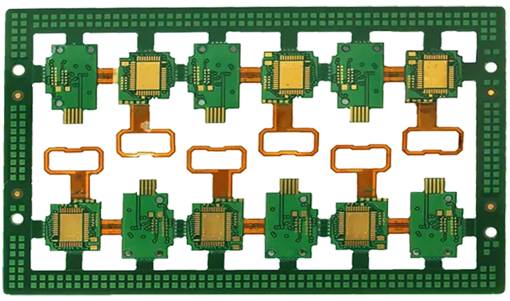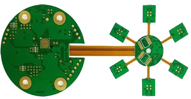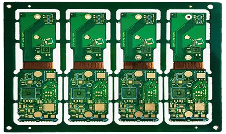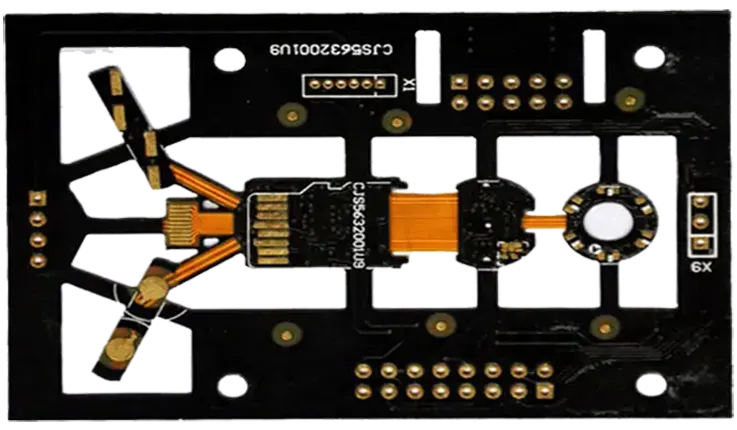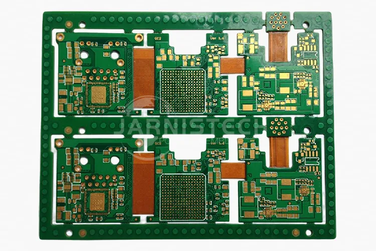
Time to Think Bigger If you’re working on your next project and want to make the leap to a more efficient, reliable, and innovative design, consider using rigid-flex PCBs. They’ll help you streamline the manufacturing process, minimize the risk of connection failure, and reduce overall weight. Plus, they open up new possibilities in space-conscious, high-performance products. So, next time you think about that tricky design problem, think about the power of rigid-flex technology to make your life easier. Your devices will thank you for it.
Rigid-Flex PCBs (Printed Circuit Boards) are revolutionizing the world of electronics by blending the strength of rigid boards with the flexibility of flex circuits. This innovative combination allows for more compact, reliable, and adaptable designs in industries ranging from aerospace to medical devices. If you’re a designer, engineer, or manufacturer, getting a solid grasp on the nuances of rigid-flex technology can seriously elevate your projects and production efficiency. Let’s dive into the details of this powerful solution and see how it’s reshaping the electronics landscape.. Buckle up, and let’s deep-dive into this tech marvel.
Understanding Rigid-flex PCBs Technology
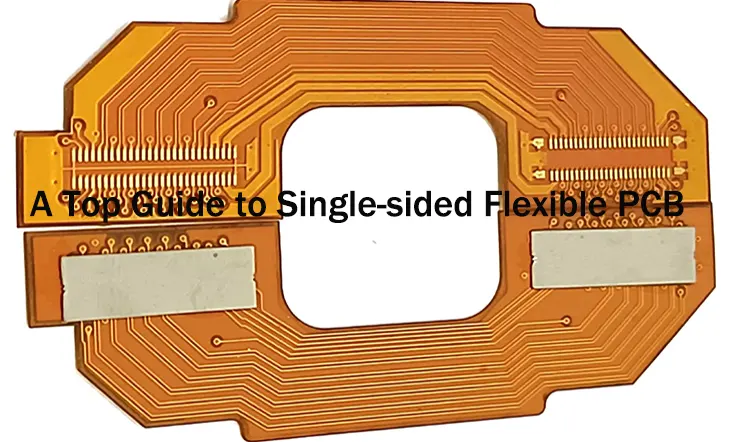
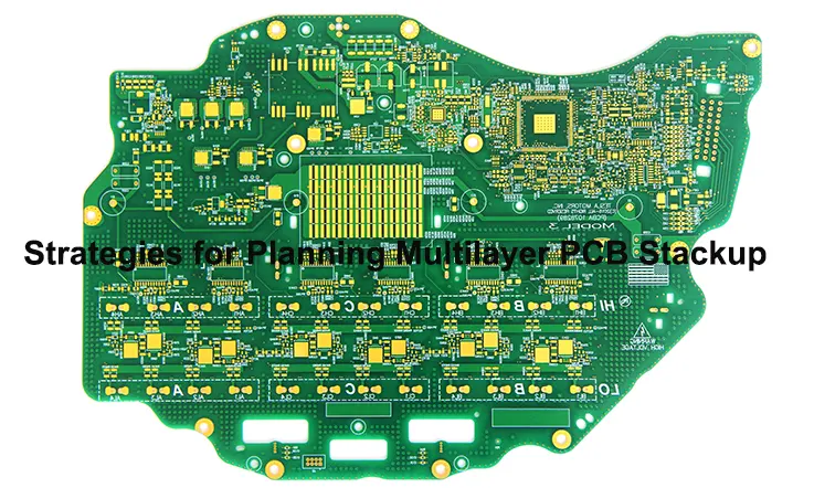
Rigid-flex PCBs are the best of both worlds—combining the durability of rigid circuits with the flexibility of, well, flexible circuits. This makes them ideal for designs that need to perform under tough conditions but still have the flexibility to bend or conform to complex shapes. Whether you’re looking to pack a bunch of components into a small device or design something that can take a beating while remaining functional, rigid-flex PCBs have got you covered.
What Sets Rigid-flex PCBs Apart?
At their core, Rigid-flex PCBs combine the durability of rigid boards with the flexibility of bendable circuits, enabling them to adapt to tight spaces and complex designs without sacrificing strength. This design is highly favored in industries like aerospace and wearables, where the ability to bend and flex without losing performance makes a big difference. Their versatility allows them to meet the rigorous demands of innovative, compact electronics.
Think of it this way: You wouldn’t want a paper-thin cable running through your laptop, right? Same idea here! You’re combining tough, stable pieces (rigid) and flexible connections (flex) that make your device both reliable and durable.
Here’s a quick look at the main differences between rigid and flexible sections of a rigid-flex PCBs:
| Attribute | Rigid Sections | Flexible Sections |
| Material | FR-4 or polyimide composites | Polyimide with copper traces |
| Functionality | Mechanical stability, housing parts | Flexibility for movement or bending |
| Applications | Processors, chips, and connectors | Cable-like functions in tight spaces |
Key Features of Rigid-flex PCBs
Rigid-flex boards are designed to perform under some serious conditions, and that’s why they’re found in critical industries like aerospace, medical devices, and electronics. Let’s take a look at some of the standout features that make rigid-flex PCBs a no-brainer for so many applications:
●Rock-Solid Reliability: Since there are no connectors between the rigid and flexible sections, the risk of failure due to physical stress or heat is minimized. That’s huge for industries like aerospace, where reliability is the name of the game.
●Compact and Sleek Design: These boards combine multiple layers into a single unit, giving designers a lot more real estate to work with without taking up extra space. Less is more when you need to fit a powerful circuit into a tiny device!
●Flexibility for Complex Shapes: Sometimes a device needs to be shaped to fit a specific space, like a wearable health monitor or a medical implant. The flexible nature of the PCB lets you design circuits that can bend and conform to the device’s structure.
How Rigid-flex PCBs Are Revolutionizing Modern Electronics?
Rigid-flex PCBs aren’t just a pretty sight—they’re revolutionizing the tech world across the board. With their ability to blend the stability of rigid circuits with the flexibility of flexible ones, these boards are enabling groundbreaking advances in design and functionality. They’ve unlocked new doors for industries like aerospace, medical devices, and wearables, driving innovations that push the limits of what was previously thought possible. In short, they’re a major leap forward, making it possible to pack more power and versatility into smaller, more efficient packages.
Here are a few industries where Rigid-flex PCBs are really making waves:
●In Aerospace: Picture this: You’re working on a satellite, and every ounce matters. Rigid-flex PCBs help reduce the weight by eliminating bulky connectors and wires, which is a huge advantage when working in space. They also hold up against extreme conditions—temperature changes, vibration, and pressure. Not a big deal for a rigid-flex board.
●In Medical Devices: Think pacemakers, hearing aids, and other implants. These devices have to be both reliable and small enough to fit inside the body. Rigid-flex PCBs pack a punch in both areas, offering the small size and durability needed for critical medical applications.
●In IoT Devices: If you’re tuned into the Internet of Things (IoT), you know the pressure to pack more power into smaller, more dependable devices. From wearables to smart home gadgets and autonomous drones, rigid-flex PCBs are making it possible to fit complex electronics into tight spaces without sacrificing reliability. These boards bring the best of both worlds—rigid and flexible—ensuring that everything stays lightweight, durable, and ready to perform at the highest level. Whether it’s a fitness tracker on your wrist or the latest drone buzzing overhead, rigid-flex PCBs are behind the scenes making it all happen.
To make the idea clearer, here’s a table showing how Rigid-flex PCBs are used across various industries:
| Industry | Application | Benefits |
| Aerospace | Satellites, Avionics | Reduced weight, resistance to harsh conditions |
| Medical Devices | Implants (pacemakers, hearing aids) | Small, durable, biocompatible |
| IoT Devices | Smartwatches, Fitness Trackers | Reliable, compact, multi-functional |
The list goes on, but you get the idea. Rigid-flex PCBs are helping engineers do more with less, and they’re making sure everything works, no matter how extreme the environment. If you’re working on a product that needs to be compact, reliable, and adaptable—rigid-flex PCBs are the way to go.
Materials and Components in Rigid-Flex PCBs
When designing a Rigid-Flex PCB, the materials you choose lay the groundwork for the performance, durability, and flexibility of the final product. These materials not only define the physical structure of your design but also ensure that it can meet the specific requirements of high-tech applications, such as aerospace, medical devices, and consumer electronics. So, let’s take a look at what makes these materials tick and how they contribute to a rigid-flex PCB that can handle the heat and keep on moving.
Flexible Materials for Rigid-flex PCBs Layers
The flexible section of a rigid-flex PCB allows the board to bend while keeping the electrical connections intact. This flexibility is a game-changer for applications in wearables, IoT devices, and compact electronics that demand both durability and adaptability.
Polyimide is the gold standard when it comes to flexible materials. This polymer resin is known for its high-temperature stability and excellent mechanical properties. Essentially, polyimide keeps things in shape, even when things get hot (literally!). This means that it can withstand the kind of heat you’d find in industrial or medical settings without melting or losing its strength.
Another material making waves is adhesive-less laminates. These laminates eliminate the need for traditional adhesives, which can sometimes be a weak link in the design. By using laminates that bond copper to the flexible base material directly, you can achieve stronger, more reliable connections. And when you’re dealing with the intricate designs that often come with rigid-flex applications, this is a big win.
Here’s a quick example: imagine designing a smartwatch where the board has to bend to wrap around the wrist. A flexible material like polyimide ensures that the board doesn’t crack or break while still allowing for complex circuits to fit on the board.
Here’s a table summarizing the main flexible materials used in rigid-flex PCBs:
| Material | Properties | Applications |
| Polyimide | High thermal resistance, flexible, durable | Wearables, flexible displays, medical devices |
| Adhesive-less Laminates | Eliminates weak bonding points, high strength | Aerospace, military electronics, RF devices |
| Other Flexible Materials | Variety of compositions, depending on the needs | Automotive, consumer electronics |
Rigid Layers and Their Roles in PCB Stack-Ups
Now, let’s talk about the backbone of any rigid-flex PCB: the rigid layers. These layers provide the structural integrity needed to house components like microchips, sensors, and connectors. Think of it like the frame of a car — it holds everything in place while allowing the flexible parts to do their thing.
For the rigid portion, FR-4 is often the go-to material. It’s a tried-and-true standard in the PCB world, offering a solid foundation for most applications. It’s tough, cost-effective, and works well in consumer electronics. However, when the requirements call for more performance—think high-frequency signals or environments with demanding thermal conditions—Rogers materials step in. These materials are specifically designed to excel in high-performance applications, like RF circuits or aerospace technologies. They offer superior thermal stability and signal integrity, ensuring your design holds up even under tough conditions.
In a typical rigid-flex stack-up, you’ll find both the flexible polyimide layers and rigid FR-4 or Rogers layers integrated into a single structure. This hybrid structure allows you to take advantage of both worlds—rigid for stability, flexible for adaptability.
Let’s break down the different types of rigid materials commonly used in rigid-flex PCBs:
| Material | Properties | Common Uses |
| FR-4 | Strong, cost-effective, standard option | Consumer electronics, low-frequency circuits |
| Rogers | High-frequency, thermal stability, expensive | Aerospace, RF communication, high-speed electronics |
| Other Rigid Materials | Varied, for specialized applications | Military, high-temperature applications |
Surface Finishes and Conductive Layers in Rigid-flex PCBs
The finishing touches on a rigid-flex PCB are more than just cosmetic; they ensure the board’s longevity and performance. A surface finish protects the PCB from corrosion and oxidation, while also improving its solderability for component attachment.
The go-to options here include ENIG (Electroless Nickel Immersion Gold), HASL (Hot Air Solder Leveling), and OSP (Organic Solderability Preservative). ENIG is the go-to for high-end designs, especially in high-density interconnect (HDI) circuits. It provides a smooth and flat surface that’s ideal for tiny, intricate connections. If you’re looking for something cost-effective, HASL may be your best bet—it’s reliable and gets the job done. On the other hand, OSP is used in more basic applications where you just need a thin coating to protect the copper.
Conductive layers, like copper foils, are typically used to create the pathways for electricity to flow. Copper is the material of choice because of its excellent electrical conductivity, ensuring that signals are transmitted without a hitch, even through the more complex designs of rigid-flex PCBs.
Here’s how it all fits together:
●ENIG is a go-to finish for high-end electronics requiring precision and long-term durability.
●HASL is a great option for standard applications that still need reliability but come with a smaller budget.
●OSP is often used in consumer goods or lower-cost devices where high-end finishes aren’t necessary.
Here’s a quick comparison of the different surface finishes used in rigid-flex PCBs production:
| Finish | Properties | Best For |
| ENIG | Gold plating, smooth, corrosion-resistant | High-frequency, military, aerospace electronics |
| HASL | Solderable, tin-lead coating | Consumer electronics, general applications |
| OSP | Thin protective organic coating | Budget-friendly consumer electronics, lower-cost applications |
Rigid-flex PCBs Design Strategies for Engineers
Designing rigid-flex PCBs comes with its own set of challenges and opportunities. Engineers need to ensure that the boards can not only perform under tough conditions but also have the flexibility needed for specific applications like medical devices, aerospace, or wearables. To make sure your design is robust and efficient, you need to follow a series of guidelines and leverage advanced tools to optimize the layout.
Design Guidelines for Reliable Rigid-flex PCBs
Designing rigid-flex PCBs requires a thoughtful approach, balancing the needs of flexibility and rigidity. The flexible sections must be able to bend without affecting the integrity of the connections, while the rigid portions provide structural stability. Achieving this balance involves careful selection of materials and layouts, ensuring that each part of the board performs its job without compromise. To ensure your rigid-flex PCB works as intended, you need to follow these foundational guidelines:
1.Proper Bend Radius: One of the most common pitfalls in rigid-flex PCB design is underestimating the bend radius. The bend radius is the minimum allowable radius for the flex section of the PCB. Exceeding this can lead to cracking or even breaking of the traces. As a rule of thumb, the bend radius should be at least 5 times the thickness of the flex PCB material. Make sure the material you’re using can handle this without losing integrity.
2.Signal Integrity: In flexible designs, signal integrity can be compromised due to the movement and bending of the board. One method to maintain signal integrity is using controlled impedance traces. Using traces that match the impedance of the circuit ensures that high-speed signals flow smoothly without reflection or noise. Additionally, ensure that the stack-up design properly accommodates the flexible sections and minimizes the risk of signal degradation.
3.Stiffeners and Reinforcements: While the flexible sections of the PCB are often the stars of the show, the rigid sections still require adequate support. Using stiffeners, like polyimide or FR-4 inserts, can help add structural integrity to the rigid areas of the PCB without affecting the flexibility of other parts.
Common Bend Radius Guidelines for Rigid-flex PCBs Design-
| Material | Recommended Bend Radius | Notes |
| Polyimide | 5x Thickness | Common flexible material |
| FR-4 | 8x Thickness | Typically used for rigid areas |
| Copper Foil | 10x Thickness | Consider for high-speed applications |
Advanced Tools for Rigid-flex PCBs Layout Design
Today’s rigid-flex PCB design is not the same as it was a decade ago, thanks to advanced CAD tools and design software. These tools allow engineers to create multi-layered, highly intricate designs that combine both rigid and flexible layers seamlessly. The following design tools are frequently used for optimal rigid-flex PCB layout:
1.CAD Software: Tools like Altium Designer and Autodesk Eagle provide engineers with intuitive interfaces to design complex rigid-flex PCBs. These platforms let you simulate and visualize how your design will behave when bent or twisted. This type of virtual prototyping saves time, prevents costly mistakes, and ensures the board’s reliability long before the manufacturing stage.
2.Layer Stack-Up Tools: Layer stack-up defines how the layers in a rigid-flex PCB are built up to form the final product. Specialized tools like Zuken and Mentor Graphics are designed to simplify the process of planning and reviewing rigid-flex stack-ups. They ensure that the electrical properties, such as impedance and capacitance, remain optimal throughout the design.
3.3D Modeling: For advanced designs, 3D modeling tools allow you to see how the board will bend in a real-world environment. With solidworks integration, for example, you can ensure that the flexible PCB sections will handle stress and movement without compromising their functionality.
Popular CAD Tools for Rigid-flex PCBs Design-
| Tool | Key Features | Best Used For |
| Altium Designer | 3D modeling, multi-layer design capabilities | High-speed, complex designs |
| Autodesk Eagle | Simple interface, large component library | Smaller, simpler designs |
| Zuken | Stack-up analysis, advanced electrical simulations | Complex multi-layer designs |
| SolidWorks | 3D integration, physical stress testing | Mechanical design integration |
Overcoming Common Design Challenges in Rigid-flex PCBs
While rigid-flex PCBs offer great advantages in compact design, there are several challenges engineers must face when creating them. Some of the most common design issues include dealing with Electromagnetic Interference (EMI), handling thermal stress, and ensuring that the flexible and rigid parts integrate seamlessly.
1.EMI Shielding: When designing rigid-flex PCBs, managing electromagnetic interference (EMI) becomes more challenging, especially as more devices rely on wireless communication. One effective way to address EMI in rigid-flex PCBs is by using copper shielding or conductive coatings on the flexible sections. Placing ground planes or signal traces that are far away from sensitive sections also helps reduce the risk of EMI.
2.Thermal Stress: The thermal management of rigid-flex PCBs can be tricky since the flexible part may experience more heat stress due to movement. Using materials with high thermal conductivity, such as ceramic-filled polyimide, and properly placing thermal vias across the board helps mitigate this issue. Additionally, it’s important to ensure that the flexible sections are well-cooled and that thermal expansion is considered during design.
3.Bend Fatigue: Flexible PCBs endure constant bending, so it’s key to select materials that can handle repeated stress without breaking down. Engineers can tackle this challenge by opting for adhesive-less laminates, which improve the PCB’s durability, and by sticking to the recommended bend radius. This approach ensures the board maintains its integrity, even after continuous flexing, preventing any failure down the line.
Materials for Managing Thermal Stress in Rigid-flex PCBs-
| Material | Thermal Conductivity (W/m·K) | Benefits |
| Polyimide | 0.12 | Flexible and durable |
| Ceramic-Filled Polyimide | 0.60 | Enhanced thermal resistance |
| FR-4 | 0.30 | Commonly used in rigid sections |
| Aluminum | 230 | High thermal conductivity for heat dissipation |
Manufacturing Rigid-flex PCBs: Step-by-Step Guide
Manufacturing rigid-flex PCBs is a multi-step process that requires precise control over materials and manufacturing techniques to ensure optimal functionality and performance. These boards are typically designed for industries that demand both high performance and compact size, such as aerospace, medical devices, and consumer electronics. To produce high-quality rigid-flex PCBs, every stage of the fabrication process must be carefully executed.
Fabrication Process for Rigid-flex PCBs
The fabrication of rigid-flex PCBs involves a number of complex steps, from the initial design to the final product. Understanding each of these steps can help you ensure that your design will be successfully manufactured. Here’s a breakdown of the key processes involved:
1.Material Selection: The process begins with selecting the right materials for both the rigid and flexible sections. For the rigid layers, FR-4 or Rogers materials are commonly used, while the flexible sections typically involve polyimide or flexible copper foil.
2.Lamination: After the materials are prepared, they are laminated together using adhesive materials or adhesive-less laminates. The lamination process bonds the layers of copper foil and the flexible base material together, creating the foundation for the PCB.
3.Drilling: Once the material stack is laminated, drilling begins. This involves creating holes for vias and component leads. For rigid-flex PCBs, drilling can be more complex due to the need to create holes in both the rigid and flexible sections. Specialized equipment is often required to drill these holes without damaging the flexible parts.
4.Etching: After drilling, etching is used to remove unwanted copper from the surface to create the desired circuit pattern. This is a delicate process since the flexible layers are more sensitive to heat and chemicals. Advanced etching techniques are used to ensure precision in both rigid and flexible layers.
5.Plating: Following etching, the next step is plating. Electroplating is commonly used to add a thin layer of copper to the vias and traces, ensuring good electrical conductivity. For rigid-flex PCBs, plating must be done carefully to avoid damaging the flexible areas.
6.Final Lamination: After the etching and plating process, the rigid-flex PCB undergoes its final lamination, where heat is applied to bond all the layers together securely. This step is where the real strength of the board comes into play, particularly at the critical points where the rigid and flexible sections meet. The heat press ensures that the materials are fused properly, providing the board with the necessary mechanical toughness to withstand the stresses it will encounter in use. This process essentially locks everything into place, ensuring the PCB’s longevity and functionality.
Common Materials Used in Rigid-flex PCBs Manufacturing-
| Material Type | Properties | Usage |
| Polyimide | Flexible, high-temperature tolerance | Flexible layers |
| FR-4 | Rigid, durable, low-cost | Rigid layers |
| Copper Foil | Conductive, thin | Circuit traces and vias |
| Rogers | High-frequency performance, stable | High-performance rigid layers |
Techniques for Multi-Layer Rigid-flex PCBs Production
For rigid-flex PCBs, one of the more advanced manufacturing techniques is the production of multi-layer boards. These boards require a higher level of complexity due to their layered design and the integration of flexible and rigid materials.
●HDI (High-Density Interconnect) Technology: HDI technology enables the creation of boards with a higher density of circuits in a smaller area. This is achieved by using fine-pitch components and advanced via technology. In rigid-flex PCBs, HDI allows more complex designs while maintaining the flexibility needed for certain applications.
●Blind and Buried Vias: One of the most common techniques used in multi-layer rigid-flex PCBs is the integration of blind and buried vias. Blind vias connect the outer layers to internal layers, while buried vias connect only internal layers, not reaching the outer layers. This allows for more efficient use of space in the design, as well as reducing the overall thickness of the board, which is particularly useful for compact applications.
●Via-in-Pad Technology: Another innovative approach is via-in-pad technology, where vias are placed directly within the pad area for components. This method increases the PCB’s density and allows for more intricate designs. However, it also requires careful management during manufacturing to avoid defects such as poor via filling or plating.
●Sequential Lamination: This process involves layering the PCB multiple times to create a multi-layer rigid-flex PCB. Each lamination step must be done carefully to ensure that the layers align correctly and that the flexible sections are not damaged during the process.
Multi-Layer Rigid-flex PCBs Manufacturing Techniques-
| Technique | Description | Benefits |
| HDI Technology | High-density designs with smaller traces and vias | Smaller footprint, more circuit density |
| Blind Vias | Vias that connect inner layers to outer layers | More efficient use of space |
| Buried Vias | Vias that connect only inner layers | Reduces overall PCB thickness |
| Via-in-Pad | Placing vias within the pads of components | Increased component density |
Quality Control in Rigid-flex PCBs Manufacturing
Ensuring that a rigid-flex PCB meets the required standards involves thorough quality control checks at every step of the process. We need to focus on various aspects, including alignment, layer bonding, and electrical performance to ensure that the final product meets both functional and structural requirements.
●Alignment Check: One of the first steps in quality control is ensuring proper alignment of the rigid and flexible layers. Any misalignment can result in issues like poor electrical contact or mechanical failure during the PCB’s use. Optical inspection systems are often used to confirm the proper alignment of holes, vias, and traces.
●Layer Bonding: The integrity of the layer bonding is another key aspect of quality control. We check to ensure that the layers, particularly the flexible layers, are securely bonded to the rigid sections without delamination. Peel strength testing is often performed to assess the strength of the bond between layers.
●Electrical Testing: Electrical testing is performed to ensure that the rigid-flex PCB performs as expected. This includes continuity testing and impedance testing to confirm that the traces are correctly connected and that the electrical performance meets the design specifications.
●Flexibility Testing: Since rigid-flex PCBs are designed to bend, testing their durability under mechanical stress is a must. To ensure they can hold up in real-world environments, we put them through bend testing and thermal cycling. These tests mimic the constant movement and temperature fluctuations the board will face in its lifetime, checking its performance and ensuring it can withstand both bending and temperature shifts without any issues. By running these tests, you make sure the board is tough enough for the long haul and won’t buckle under pressure.
Common Quality Control Tests for Rigid-flex PCBs-
| Test Type | Purpose | Testing Method |
| Alignment Test | Ensure correct layer alignment | Optical inspection and alignment tools |
| Peel Strength Test | Check the strength of the layer bonding | Mechanical testing of adhesive strength |
| Electrical Continuity | Confirm the traces and vias are electrically connected | Automated continuity and impedance testing |
| Flexibility Test | Evaluate the board’s ability to flex without failure | Bending and thermal cycling tests |
Assembly Processes for Rigid-flex PCBs
Assembling rigid-flex PCBs requires precision and an understanding of their unique structure. These boards combine flexible and rigid materials, making them perfect for compact devices where space and reliability are top priorities. Let’s break down the techniques, testing procedures, and challenges involved in assembling these versatile circuit boards.
SMT and Through-Hole Assembly Techniques
Surface Mount Technology (SMT) and through-hole methods are the primary techniques used to assemble components onto rigid-flex PCBs. The hybrid nature of these boards demands careful handling to prevent damage, especially in the flexible sections.
1.SMT Assembly:
●Process: Components are placed on the rigid sections using automated pick-and-place machines. Solder paste is applied to ensure secure connections during reflow soldering.
●Considerations: Reflow ovens must be programmed with profiles suitable for the board’s flexible layers to avoid thermal damage. Stiffeners are often applied to support the flex sections during assembly.
●Applications: Ideal for dense, compact designs with small components like IoT devices and wearables.
2.Through-Hole Assembly:
●Process: Components with leads are inserted into pre-drilled holes and soldered manually or using wave soldering. This technique is preferred for connectors and larger components requiring mechanical strength.
●Challenges: Proper alignment and support for the flexible regions during soldering to avoid misalignment or damage.
●Applications: Commonly used in high-reliability designs like aerospace systems.
Comparison of SMT and Through-Hole Assembly for Rigid-flex PCBs-
| Aspect | SMT Assembly | Through-Hole Assembly |
| Component Size | Small components | Larger components |
| Automation Level | Highly automated | Semi-automated or manual |
| Use Case | High-density circuits | Mechanical stability and durability |
| Challenges | Heat sensitivity in flex areas | Misalignment during soldering |
Testing Assembled Rigid-flex PCBs for Reliability
Once the assembly is complete, testing ensures that the board performs as intended under operational conditions. With the combination of rigid and flexible sections, rigorous testing is necessary to validate both electrical performance and mechanical durability.
1.AOI (Automated Optical Inspection):
●Used to inspect solder joints and component placement. AOI systems detect defects such as misaligned components or insufficient solder paste.
●Particularly useful for SMT sections where component density is high.
2.X-Ray Inspection:
●Non-destructive testing to check for hidden defects, such as voids in solder joints or poor via connections.
●Essential for multi-layer boards and areas with blind/buried vias.
3.Functional Testing:
●Simulates real-world operating conditions to ensure the board performs as expected.
●Includes electrical testing (continuity and impedance) and mechanical testing (flexibility and thermal cycling).
4.Environmental Testing:
●Involves subjecting the board to thermal shock, vibration, and humidity to confirm durability in harsh conditions.
●When working in industries like aerospace or automotive, ensuring that components can endure the demanding conditions is a must.
Common Testing Methods for Assembled Rigid-flex PCBs-
| Test Type | Purpose | Example Tools/Methods |
| AOI | Inspects for visual defects | Automated inspection machines |
| X-Ray Inspection | Detects internal flaws in solder joints | 3D X-ray imaging systems |
| Functional Testing | Verifies electrical and mechanical performance | Multimeters, thermal chambers |
| Environmental Testing | Ensures durability under stress | Vibration and temperature cycling setups |
Soldering Challenges in Rigid-flex PCB Assembly
Soldering is one of the trickiest steps in assembling rigid-flex PCBs due to the delicate nature of the flexible sections. Heat management, solder joint integrity, and mechanical stress are common challenges.
1.Heat Management:
●Flexible sections are prone to heat damage. Using low-temperature solder alloys and controlled reflow profiles can mitigate risks.
●Stiffeners or fixtures are often used to provide thermal mass and support.
2.Joint Integrity:
●Flexible regions are more susceptible to mechanical stress, which can cause solder joint cracking or failure. Reinforced soldering techniques, such as underfilling, help prevent these issues.
3.Preventing Warpage:
●Rigid-flex PCBs can warp during soldering due to uneven heating. Using proper panelization and thermal profiling minimizes deformation.
4.Flux Residue Removal:
●Residue can accumulate in the flexible sections, leading to long-term reliability issues. Cleaning with appropriate solvents ensures a pristine assembly.
Common Soldering Challenges and Solutions-
| Challenge | Description | Solution |
| Heat Sensitivity | Flexible layers damaged by high heat | Low-temp solder, custom reflow profiles |
| Joint Cracking | Mechanical stress on solder joints | Reinforcement with underfill |
| Board Warpage | Deformation during soldering | Controlled thermal profiles, fixtures |
| Residue Buildup | Flux residue in flex sections | Proper cleaning with solvents |
Quality Assurance and Testing for Rigid-flex PCBs
The reliability of rigid-flex PCBs hinges on thorough quality assurance and testing protocols. From evaluating mechanical durability to ensuring electrical performance, each step contributes to delivering a PCB that meets rigorous industry demands.
Durability Testing for Rigid-flex PCBs
Durability testing is central to determining whether rigid-flex PCBs can withstand harsh operating conditions. These assessments often include:
●Vibration Testing: Simulating real-world mechanical stress to verify the PCB can endure oscillations, common in automotive and aerospace systems.
●Bending Analysis: Examining how flexible regions perform under repeated flexing. For example, in wearables, PCBs endure hundreds of bending cycles daily, requiring robust materials and layouts.
●Thermal Cycling: Exposing boards to fluctuating temperatures to gauge resistance to thermal expansion and contraction. A test might involve 100 cycles between -40°C and 125°C, replicating the conditions faced by outdoor devices.
| Test Type | Purpose | Standard Metrics |
| Vibration Testing | Ensure resistance to motion | Frequency ranges: 20 Hz to 2000 Hz |
| Bending Analysis | Validate flex reliability | Cycle count: ≥10,000 flexes |
| Thermal Cycling | Assess temperature resilience | Transition time: 10°C/min |
Electrical Performance Testing in Rigid-flex PCBs
To ensure reliable data transmission and power delivery, electrical performance tests focus on:
●Signal Integrity Checks: Using Time-Domain Reflectometry (TDR) to detect issues like signal reflections or attenuation, ensuring data transmission remains pristine.
●Impedance Control Verification: Essential for high-speed circuits, this ensures traces meet design impedance requirements. For instance, a mismatched impedance could cause data errors in communication devices.
●Continuity Testing: Verifying electrical connectivity across all traces and vias.
Engineers frequently employ automated test equipment (ATE), reducing manual errors and accelerating the testing phase.
Preventing Common Failures in Rigid-flex PCBs
Failures in rigid-flex PCBs often stem from design oversights or material inconsistencies. Proactive measures include:
●Cracking Prevention: Using materials with high elongation properties and avoiding sharp corners in trace layouts.
●Delamination Mitigation: Ensuring proper bonding between layers through optimized lamination pressures and temperatures.
●Short-Circuit Avoidance: Employing precise soldering techniques and regular inspection to identify and address solder bridges early.
Case Study Example:
A medical device manufacturer reduced short circuits by implementing a double-pass solder inspection protocol, resulting in a 30% improvement in board reliability.
Comparison of Rigid, Flex, and Rigid-flex PCBs
To decide between rigid, flex, and rigid-flex PCBs, it’s crucial to weigh their differences in design, manufacturing methods, and cost. Understanding these factors will help you choose the most fitting option for your project. Let’s dive deeper into these aspects.
1.Design Considerations
| Feature | Rigid PCBs | Flex PCBs | Rigid-flex PCB |
| Flexibility | No flexibility; ideal for static designs. | Fully flexible, enabling 3D designs and dynamic movement. | Combines rigid and flexible sections for hybrid designs. |
| Stack-Up | Simple single or multi-layer designs. | Requires careful layer alignment and stress considerations. | Complex stack-ups integrating rigid and flex layers. |
| Design Tools | Standard PCB CAD software suffices. | Requires specialized CAD tools for flex and dynamic simulations. | Advanced tools needed for hybrid designs, including stress and bending analysis. |
| Applications | Computing, industrial devices. | Wearables, medical implants. | Aerospace, automotive, and medical systems. |
2. Manufacturing Process
| Feature | Rigid PCBs | Flex PCBs | Rigid-flex PCBs |
| Materials | FR-4 and epoxy laminates. | Polyimide and adhesive-less laminates. | FR-4 for rigid sections, polyimide for flex. |
| Fabrication | Standard drilling, etching, and lamination. | Includes unique processes like roll-to-roll fabrication. | Combines rigid and flex fabrication steps, with special lamination techniques. |
| Challenges | Minimal manufacturing complexity. | Precision required for thin layers and bending. | Ensuring proper bonding between rigid and flex layers. |
| Testing | Electrical testing for multi-layer stacks. | Requires dynamic flex testing and strain analysis. | Additional tests for mechanical and electrical integrity. |
3. Cost Analysis
| Aspect | Rigid PCBs | Flex PCBs | Rigid-flex PCBs |
| Material Cost | Lowest due to standard materials. | Higher due to specialized flexible substrates. | Highest due to hybrid material usage. |
| Fabrication | Cost-effective and efficient. | Costlier due to intricate processes. | Most expensive, combining both rigid and flex processes. |
| Production Volume | Scales well for high-volume production. | Economies of scale impact less pronounced. | Small batch production incurs higher costs. |
| Prototyping | Affordable for early design stages. | Relatively higher due to unique requirements. | Prototyping is the most expensive due to complexity. |
Comprehensive Comparison
| Aspect | Rigid PCBs | Flex PCBs | Rigid-flex PCBs |
| Flexibility | None | Full flexibility | Hybrid |
| Material Cost | Low | Moderate to high | High |
| Manufacturing Complexity | Low | Moderate to high | High |
| Prototyping Cost | Affordable | Expensive | Most expensive |
| Applications | Static designs | Dynamic or compact designs | Complex hybrid designs |
How Cost Optimization for Rigid-flex PCBs?
Rigid-flex PCBs, recognized for their toughness and adaptability, come with a distinct cost breakdown shaped by material selection, production methods, and manufacturing scale. To get the most out of your budget while ensuring optimal performance, understanding these factors and applying smart planning strategies is key to hitting the sweet spot.
Factors Influencing Rigid-Flex PCBs Costs
Several variables shape the cost structure of rigid-flex PCBs. Here’s a breakdown of the most impactful factors:
Material Selection-
High-performance materials like polyimide for flexible layers and FR-4 for rigid layers significantly influence costs. Opting for adhesive-less laminates or specific copper thicknesses can also increase expenses. Custom materials with specialized properties, such as high-temperature resistance, typically add premium costs.
Design Complexity-
Multi-layer designs with features such as blind/buried vias and controlled impedance require advanced equipment and extended processing time. This is particularly evident in designs demanding stringent electrical performance for high-frequency applications.
Production Volume-
Unit costs decrease significantly with larger production batches due to economies of scale. However, initial setup charges for custom tooling and design adaptation make smaller runs more expensive per unit.
| Cost Factor | Impact | Examples |
| Material Choice | Higher quality increases costs | Polyimide flex layers vs. standard FR-4 |
| Layer Count | More layers mean higher costs | 10+ layers with blind/buried vias |
| Batch Size | Larger batches reduce unit costs | 1000+ units benefit from volume discounts |
Strategies for Cost-Efficient Rigid-Flex PCBs Production
Cost-efficient production requires a combination of smart design practices and effective communication with PCB manufacturers. Here’s how you can keep costs in check:
1.Collaborate with Manufacturers Early-
Engaging a PCB manufacturer during the design phase can help streamline production. For instance, ensuring the bend radius of flexible sections adheres to manufacturing capabilities avoids costly redesigns.
2.Optimize Layer Stack-Up-
Simplify the design where possible by reducing unnecessary layers or using shared ground planes. Avoid excessive copper usage unless the application specifically demands high current handling.
3.Choose Standardized Materials-
Stick to materials commonly stocked by manufacturers to minimize lead times and costs. Custom materials or exotic specifications often incur surcharges.
4.Batch Prototyping-
Combining prototypes with larger production runs can save on setup costs. A hybrid approach where prototypes are tested for DFM (Design for Manufacturability) before scaling to mass production ensures cost control.
| Strategy | Benefit | Example |
| Early Manufacturer Input | Reduces design revision costs | Adjusting flex area bend radius |
| Layer Optimization | Reduces material usage | Shared ground layers |
| Standard Material Use | Lowers procurement costs | Polyimide stocked by multiple suppliers |
Why Choose JarnisTech as Your Rigid-flex PCBs Partner?
JarnisTech stands out in the PCB industry for its ability to craft high-quality rigid-flex solutions tailored to diverse applications. With a foundation built on advanced technology, customer collaboration, and industry-specific insights, we offer unparalleled manufacturing and engineering expertise.
JarnisTech’s Capabilities at a Glance
Our rigid-flex PCB offerings are designed to meet the unique demands of modern electronics, emphasizing versatility and precision:
| Feature | Rigid PCBs | Flexible PCBs |
| Layer Capacity | Up to 60 layers | Up to 16 layers |
| Specialized Features | Blind and buried vias, advanced stack-ups | Accepts aluminum, PI, FR-4 stiffeners |
| Applications | Aerospace, robotics, medical, military | High-flex applications, wiring harness replacement |
What Sets JarnisTech Apart?
1.Customized Solutions for Demanding Applications-
Our rigid-flex designs are crafted to thrive in extreme environments like aerospace systems or robotic controls, ensuring performance without compromise. For example, circuits intended for medical devices or military hardware require precision that only experienced manufacturers like us can deliver.
2.Engineering Support From Start to Finish-
Our dedicated engineering team works closely with clients from the conceptual phase through to production. Whether you need help optimizing bend radius or integrating stiffeners, we provide guidance to ensure a seamless process.
3.Cost-Effective Alternatives to Traditional Wiring-
By replacing traditional wire harnesses with rigid-flex PCBs, clients achieve significant reductions in weight, complexity, and costs. For instance, a customer in the robotics industry reduced their assembly time by 20% using our custom solutions.
4.Dependable Quality Control-
Every board goes through a rigorous inspection process, from electrical testing to layer bonding analysis, ensuring top-notch reliability. We adhere to global standards and possess certifications to back our claims.
Industries We Serve
●Aerospace: Advanced rigid-flex solutions for lightweight, high-reliability applications.
●Medical: Miniaturized designs for surgical tools and imaging equipment.
●Military: Robust designs for radar systems and unmanned vehicles.
●Robotics: Flexible circuits optimized for dynamic movement.
Ready to Partner With JarnisTech?
Take the guesswork out of your PCB project. Send your files to [email protected], and we’ll provide a tailored solution with a competitive quote. Let’s build the foundation of your next breakthrough together!
FAQs About Rigid-flex PCBs
Can rigid-flex PCB handle high-current applications?
Yes, but it requires careful design to manage heat dissipation, appropriate copper thickness, and effective power distribution.
How do rigid-flex PCB differ in design constraints compared to traditional PCBs?
Designers must account for bend radius, dynamic flex cycles, and material layer compatibility to prevent mechanical failures.
What is the typical shelf life of a rigid-flex PCBs?
When stored in optimal conditions (low humidity and temperature-controlled), rigid-flex PCBs can maintain functionality for up to 10 years.
Are rigid-flex PCB RoHS-compliant?
Yes, most PCB manufacturers offer RoHS-compliant options, ensuring the absence of harmful substances like lead and mercury.
How are flexible sections of rigid-flex PCBs protected during assembly?
Flexible sections are often covered with stiffeners or specialized materials to prevent damage during soldering and handling.
What software tools are recommended for designing rigid-flex PCBs?
Industry-standard tools like Altium Designer, OrCAD, and KiCad provide advanced features tailored for rigid-flex PCB layouts.

