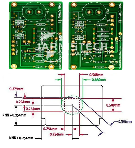
As we know, PCB tolerances are present in every PCB manufacturing aspect. When you design a new product it is done with an exact set of dimensions in your mind. They are also known as nominal dimensions. The tighter or smaller precise the tolerance the greater the price or the longer the time to manufacture will be. In the production of industrial printed boards, There are international standards, and these are in addition used to determine the PCB tolerances.
In the world of high-precision PCB manufacturing, tolerances are far more than a set of numbers—they’re the backbone of quality, reliability, and performance. When designing or producing printed circuit boards, every minute deviation can mean the difference between a flawless product and one that fails to meet the rigorous demands of modern electronics.
The Strategic Importance of Tolerances in PCB Manufacturing
When diving into PCB manufacturing, tolerances are often seen as a behind-the-scenes factor. However, their strategic importance is immense. Whether you’re developing a basic consumer electronics board or a high-frequency application for 5G systems, the precision of your PCB tolerances directly influences everything from production cost to long-term product reliability. As manufacturing techniques evolve, so too do the challenges and opportunities related to these tolerances. By understanding their impact, you can avoid costly mistakes, optimize designs, and create products that meet market expectations faster and more efficiently.
Why Tolerances Matter More Than You Think?
It’s easy to overlook the tolerance aspect of PCB design, especially when you’re focused on aesthetics or functionality. However, a small tolerance deviation can escalate into a major issue that compromises not only your board’s electrical performance but also its manufacturability and overall cost. For example, a hole size tolerance that’s too wide can result in components that don’t fit snugly, leading to unreliable solder joints or component misalignment. On the other hand, too tight a tolerance can increase the manufacturing costs and time-to-market, slowing down production and raising prices.
PCB tolerances affect a wide array of elements such as hole sizes, trace widths, and layer alignment. If your hole sizes aren’t specified correctly, the components could either be too loose or too tight, creating issues during assembly. Similarly, if your trace widths aren’t designed within the right tolerances, current might not flow as expected, which can lead to overheating or signal degradation. The time-to-market is also impacted because tight tolerances often require more meticulous production processes, potentially extending the manufacturing timeline.
For example, when teflon PCBs are involved, ensuring precise tolerances can prevent costly mistakes. Teflon, known for its high-frequency performance, requires exceptional precision to ensure that signal integrity isn’t compromised by manufacturing defects. This is where understanding tolerance helps not only in crafting high-performance boards but also in optimizing production time and controlling costs.
How Tolerances Influence Product Lifecycle and Scalability?
A seemingly minor deviation in PCB tolerances can have lasting effects on a product’s lifecycle and scalability. As PCBs are integrated into larger systems, any tolerance mismatch could result in unexpected failures, impacting everything from signal processing to thermal management. For instance, when trace widths and layer alignment tolerances aren’t followed properly, electrical signals can become distorted, leading to faulty performance and premature failure.
Moreover, Scaling a PCB design from prototype to mass production hinges on precision and consistency in tolerances. . As you move from a prototype to a full-scale production run, any inconsistency in tolerances could disrupt the manufacturing process, leading to increased scrap rates and slower production times. By maintaining the right tolerance values from the outset, we ensure that our products are both scalable and reliable as they move from design to mass production.
Let’s take the example of a high-frequency PCB used in 5G systems. Even a 0.1mm tolerance in trace widths can affect the signal integrity, especially at higher frequencies. For such products, tight tolerances are non-negotiable to ensure the board performs correctly in the final application. This is not just a one-off concern—poor tolerance management affects long-term product lifecycle, potentially requiring redesigns or repairs over the product’s life.
The Intersection of Tolerances and Design Innovation
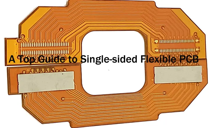
As PCB design advances, tolerance limits are constantly being pushed. Innovations like flexible PCBs or boards for high-frequency applications challenge the traditional tolerance boundaries. Flexible PCBs, for instance, require careful management of layer alignment tolerances to ensure they remain durable and functional when bent or flexed. If the tolerances are off, the board could crack or degrade, significantly affecting its performance.
Moreover, high-frequency PCBs require even more stringent tolerance specifications to preserve signal integrity. For instance, in 5G networks, the signals being transmitted operate at millimeter-wave frequencies that are incredibly sensitive to even minor variations in trace width or spacing. A trace width tolerance that’s too large could disrupt these high-speed signals, leading to data loss or communication failure.
In this today industry, design innovations are increasingly intertwined with tolerance management. PCB designers and manufacturers must work closely to balance design goals with manufacturability, ensuring that cutting-edge designs can still be produced to meet the highest performance standards without exceeding cost and production time constraints.
Impact of Tolerance Variations on PCB Performance and Scalability
| Tolerance Type | Impact of Deviation | Example Applications | Tolerance Range |
| Hole Size Tolerance | Misalignment of components, poor soldering | Consumer electronics, automotive systems | ±0.05mm to ±0.10mm |
| Trace Width Tolerance | Signal degradation, overheating | High-frequency applications, 5G, IoT | ±0.05mm to ±0.2mm |
| Layer Alignment Tolerance | Signal distortion, electrical shorts | Multilayer PCBs, medical devices | ±0.1mm |
| PCB Thickness Tolerance | Bending issues, mechanical failure | Flexible PCBs, wearable tech | ±0.1mm to ±0.2mm |
Pro Tip: As you design and manufacture PCBs with increasingly complex features, keep a close eye on your tolerances. If you’re working on flexible designs or high-frequency boards, even a slight deviation can lead to signal loss or product failure. Always consult with your PCB manufacturer to ensure that the tolerances match the fabrication’s requirements and that both quality and scalability are achieved from the start.
Types of PCB Tolerances in Manufacturing
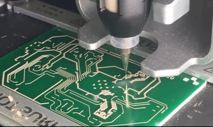
PCB tolerances set the limits for acceptable deviations in parameters like hole sizes, trace widths, and board thickness. These numbers aren’t picked out of thin air—they ensure the board works as intended, whether it’s powering your phone, steering a car, or running medical equipment. Understanding the various tolerances involved is the ticket to building a product that performs well without breaking the bank. Too-tight tolerances can crank up costs and complicate production, while too-loose ones risk throwing performance out the window. Let’s break down the main types of tolerances in PCB manufacturing and how they shape the process.
Hole Size and Drill Tolerances in PCBs
Hole size tolerances are a big deal in PCB manufacturing. They define how much wiggle room is allowed in the diameter of drilled holes used for vias, component leads, and other connections. Even a slight deviation can throw a wrench into the assembly process, leading to loose fits or misalignments that impact the board’s functionality. Keeping these tolerances in check ensures a smooth fit during assembly and reliable electrical connections across the board.
In particular, the via hole tolerance needs to be precise to ensure the proper electrical connection between layers and the effective functioning of the device. Variations can result in weak signals, excessive resistance, and poor component placement, leading to defects that may not be detected until later in the production cycle.
Hole Size and Drill Tolerances in PCBs-
| Hole Size (in mm) | Tolerance Range | Impact of Deviation | Common Applications |
| 0.2 – 0.5 | ±0.05mm to ±0.1mm | Too large: loose components; Too small: improper fit, stress | Through-hole components, vias |
| 0.5 – 1.0 | ±0.1mm | Too large: excess copper plating; Too small: assembly failure | High-frequency circuit boards |
| 1.0 – 2.0 | ±0.2mm | Too large: possible short-circuit; Too small: component misalignment | Power electronics, automotive PCBs |
Trace Width and Spacing Tolerances in High-Density PCBs
When designing high-density PCBs, the management of trace width and spacing tolerances becomes a whole new ball game. With smaller traces and tighter spacing, we can cram more components into a smaller space. But the more compact the design, the more sensitive it becomes to small variations in tolerance. Even the tiniest misstep can lead to electrical issues, short circuits, or manufacturing headaches. So, while pushing the limits of density, it’s key to maintain precision in these dimensions to avoid turning a great design into a costly failure down the line.
Incorrect trace widths or spacing can lead to issues like signal degradation or even failure to pass electrical signals altogether, which could result in a complete system breakdown. Particularly in high-frequency applications like 5G and IoT, maintaining tight trace width and spacing tolerances ensures that the PCB works efficiently and that the signals stay intact.
Trace Width and Spacing Tolerances for High-Density PCBs-
| Trace Width (in mm) | Spacing (in mm) | Tolerance Range | Impact of Deviation | Common Applications |
| 0.05 – 0.1 | 0.05 – 0.1 | ±0.05mm to ±0.1mm | Narrow traces: reduced signal integrity, potential cross-talk | High-frequency PCBs, 5G boards |
| 0.1 – 0.15 | 0.1 – 0.2 | ±0.1mm | Wider traces: loss of signal quality, increased impedance | High-density boards, IoT circuits |
| 0.2 – 0.3 | 0.3 – 0.4 | ±0.2mm | Lowered performance, higher risk of signal reflection | Power systems, automotive applications |
Thickness and Flatness Tolerances for PCB Boards
When it comes to PCB thickness and flatness tolerances, they have a big hand in making sure the board holds up structurally. If the thickness varies too much, it can mess with the mounting of components and throw off the whole performance, especially when dealing with multi-layer designs. Flatness tolerance is no less important—without it, component alignment gets tricky, and there’s a real risk of stress being placed on components when they’re soldered in place. So, getting these dimensions right is more than just a detail—it’s the difference between a flawless build and a board that’s just begging for trouble.
For flexible PCBs, the thickness and flatness need to be especially controlled to maintain the flexibility required for bending and fitting into tight spaces. Boards that are too thick may lose flexibility, and boards that are too thin may lack the strength required for the intended use. Likewise, keeping the flatness in check is key to making sure the board doesn’t warp, ensuring it keeps working like a charm throughout its entire lifespan. Without those tolerances dialed in, you’re looking at a board that just won’t do the job right.
Thickness and Flatness Tolerances for PCB Boards-
| Thickness (in mm) | Tolerance Range | Impact of Deviation | Common Applications |
| 0.2 – 0.4 | ±0.1mm | Too thick: reduces flexibility, difficult assembly; Too thin: weak integrity | Flexible PCBs, consumer electronics |
| 0.5 – 1.0 | ±0.2mm | Too thick: reduced performance in high-speed applications; Too thin: lack of mechanical stability | Automotive, aerospace, medical devices |
| 1.0 – 1.5 | ±0.3mm | Too thick: more difficult to mount components; Too thin: possible breakage | Power distribution boards, industrial systems |
Factors Influencing PCB Tolerances
When designing and manufacturing printed circuit boards, tolerances are not just an afterthought—they’re built into the fabric of the design and production process. These tolerances ensure that each board fits together as intended, from precise hole sizes to trace widths, ensuring the final product is reliable and performs as expected.
Understanding the factors that influence PCB tolerances helps minimize defects, boost product yields, and ensure long-lasting functionality. These factors include material choices, production techniques, and environmental conditions during manufacturing. Each of these elements can affect the precision of the finished product. In the following sections, we’ll explore how each of these factors contributes to the overall quality of your PCB design and manufacturing process.
Material Selection and Its Impact on PCB Tolerances
The material you choose for your PCB is one of the biggest influences on the achievable tolerances. Think about it: when you select a material like FR4 (the most commonly used PCB material), you are setting the stage for the level of precision your board can achieve. Different materials expand and contract at varying rates when subjected to heat and environmental changes, which can affect the overall dimension stability of the PCB.
Take Teflon as an example—it’s known for its high-frequency performance and low dielectric constant, making it ideal for advanced applications like 5G or aerospace circuits. However, Teflon is more challenging to work with, and getting tight tolerances with this material can be trickier due to its unique chemical properties and higher cost. Similarly, flexible substrates present their own challenges: they require specialized processes to maintain tight tolerances, especially when bending or flexing the board.
Material Selection and Impact on Tolerances-
| Material Type | Dielectric Constant | Tolerance Achievability | Applications | Challenges |
| FR4 | 4.5 – 5.0 | ±0.1mm to ±0.2mm | Consumer electronics, automotive | Shrinkage during heat, limited high-frequency use |
| Teflon | 2.1 – 2.3 | ±0.05mm | High-frequency, 5G | Expensive, difficult to handle, shrinkage issues |
| Flexible Substrates | 3.0 – 4.5 | ±0.1mm to ±0.2mm | Wearable tech, bendable boards | Flexing causes dimensional instability |
The Role of Manufacturing Processes in Achieving Tighter Tolerances
When it comes to achieving tighter tolerances in PCB production, the manufacturing process is where the magic happens. From etching to plating, the steps taken to shape and assemble the board directly impact the precision of the finished product.
For instance, in etching, the accuracy with which traces are etched onto the board can affect the trace width and spacing tolerances. If the etching process isn’t fine-tuned, you may encounter issues like trace undercutting or excessive trace width. Similarly, plating can influence hole sizes and their associated tolerances. As copper plating builds up on the walls of the drilled holes, it must be controlled within specific limits to prevent holes from becoming too narrow or uneven, which could result in connection issues.
PCB Manufacturers use high-precision equipment to achieve these tolerances, but even the most cutting-edge technology is still susceptible to human error. Every step—whether it’s etching, plating, or drilling—requires strict attention to detail to maintain consistent, tight tolerances across the entire batch of PCBs.
Manufacturing Processes Impact on PCB Tolerances-
| Process Type | Impact on Tolerances | Challenges | Tools and Techniques |
| Etching | Trace width and spacing | Risk of undercutting or irregular widths | Laser etching, photolithography |
| Plating | Hole diameter and uniformity | Uneven plating, copper buildup affecting hole size | Electroplating, selective plating |
| Drilling | Hole size and alignment | Misalignment, drill bit wear can affect precision | High-speed drilling machines |
Environmental Factors Impacting PCB Tolerances
Environmental conditions can significantly impact PCB tolerances, often in ways that aren’t immediately obvious. Factors like temperature, humidity, and air quality affect the material properties of the PCB, which in turn can alter the dimensions and overall quality of the board. For example, thermal expansion can lead to changes in the size and shape of the PCB during manufacturing, especially when exposed to high or fluctuating temperatures. Understanding these environmental factors helps ensure that the board maintains its integrity and functions as expected, even after it’s been put through various stages of production.
For instance, high humidity can cause the substrate material to absorb moisture, which affects its dimensions and stability. On the flip side, extreme temperatures can cause materials to contract or expand, leading to changes in hole sizes and trace widths. During manufacturing, the reflow soldering process—which involves heating the board to temperatures as high as 250°C—can induce thermal stress. If the cooling process is not controlled properly, the PCB can warp or distort, further affecting the tolerance.
One of the best ways to minimize the impact of environmental factors is through environmentally controlled production facilities, which can maintain consistent temperature and humidity levels throughout the entire manufacturing process.
Environmental Factors and Their Impact on PCB Tolerances-
| Factor | Effect on Tolerances | Mitigation Strategies | Common Impact Areas |
| Temperature | Expansion or contraction of materials | Use of temperature-controlled production areas | Hole sizes, trace width |
| Humidity | Moisture absorption by PCB materials | Use of dehumidifiers, moisture-proof packaging | Material shrinkage, warping |
| Air Quality | Dust and particulate contamination | Cleanroom environments, air filtration systems | Surface finish, etching precision |
Challenges in Maintaining PCB Tolerances
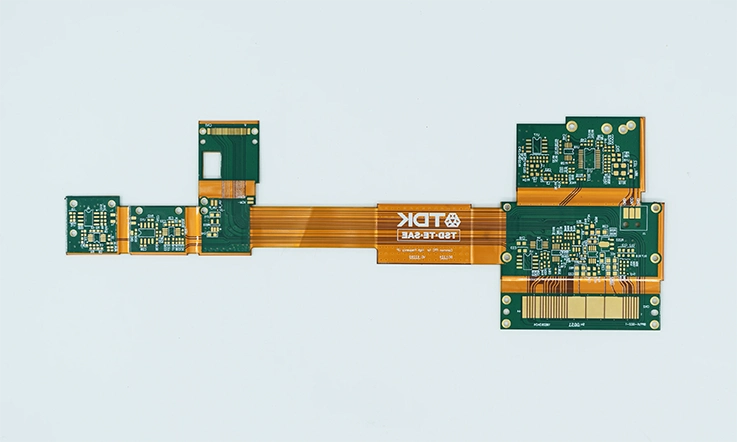
As technology progresses, keeping tolerances tight in PCB manufacturing presents growing challenges. Every stage—from material selection to the assembly process—requires careful attention. A minor misstep in any of these stages can lead to defects or problems with the final product. Understanding how to manage these challenges is a must for creating reliable boards, particularly when working with multi-layer designs, dense layouts, or sensitive components. Precision is a must at every stage to ensure a well-functioning end product.
Thermal Expansion and Warpage in PCB Manufacturing
In high-performance PCBs, particularly those used in 5G or automotive applications, thermal expansion is a major challenge. When temperature fluctuations occur during production or in the operational environment, materials like FR4 and Teflon expand or contract at different rates. This can alter the PCB’s dimensions and, in turn, its tolerances.
Thermal stress during the reflow soldering process, for instance, can cause the board to warp. As the PCB cools, different sections of the board might contract at different rates, leading to misalignment of holes or traces. This warping can seriously affect the signal integrity and reliability of the final product.
PCB Manufacturers often address these challenges by employing controlled thermal environments during the reflow process and using high-precision materials that can withstand temperature changes without significant distortion.
Thermal Expansion and Its Effect on PCB Tolerances-
| Material | Coefficient of Thermal Expansion (CTE) | Impact on Tolerances | Challenges |
| FR4 | 14-16 ppm/°C | Expansion/contraction of traces | Temperature fluctuations causing trace misalignment |
| Teflon | 30-40 ppm/°C | Risk of warping, high-frequency issues | Costlier material with low dimensional stability |
| Polyimide | 10-20 ppm/°C | Possible hole misalignment | Challenging to maintain precision under heat |
Mechanical Stress and the Risk of Tolerance Deviation
Handling and assembly of PCBs can introduce mechanical stress, which is another significant challenge when it comes to maintaining tight tolerances. Whether it’s during PCB testing, component mounting, or final assembly, external forces can bend, flex, or distort the board, leading to deviations in hole sizes, trace alignment, and layer misregistration.
For instance, if a PCB is handled too roughly during testing or assembly, it could cause microfractures in the copper traces or delamination between layers, which compromises the board’s integrity. Even small deviations in mechanical handling can cause a ripple effect, where slight misalignments accumulate into a larger issue down the line.
Proper handling techniques and automated assembly systems that minimize manual contact with the PCB are key to mitigating mechanical stress. Additionally, ensuring that components are mounted and soldered without excessive force is another way to minimize the risk of tolerance issues.
Impact of Mechanical Stress on PCB Tolerances-
| Stress Source | Effect on Tolerances | Common Areas Affected | Mitigation Strategies |
| Handling | Flexing or bending, trace misalignment | Hole sizes, trace width | Use of mechanical handling robots, proper training for assembly teams |
| Soldering | Overheating, uneven cooling | Warping, trace distortion | Precision soldering equipment, controlled temperature processes |
| Assembly Pressure | Compressive stress causing deformation | Component misplacement, via damage | Automated placement machines, lightweight tools for handling |
The Challenge of Maintaining Tolerances in Multi-Layer PCBs
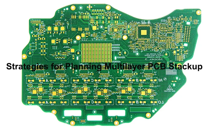
The multi-layer PCB is a marvel of modern electronics, but with its complexity comes the challenge of maintaining precise tolerances. Each layer must align perfectly to ensure the electrical connections between them are accurate and reliable. The more layers you add, the more difficult it becomes to ensure consistency across the board.
For example, in high-density PCBs used in consumer electronics, the thickness and flatness of each layer can vary, leading to misregistration between layers. Small discrepancies can lead to short circuits, open circuits, or signal degradation, especially in high-frequency designs.
We need to implement strict layer-to-layer alignment checks and often use laser drilling or via filling techniques to ensure that every layer is perfectly aligned. The use of advanced inspection tools such as Automated Optical Inspection (AOI) and X-ray inspection can help identify any misalignments early in the process.
Challenges in Multi-Layer PCB Tolerances-
| Layer Factor | Effect on Tolerances | Common Issues | Mitigation Strategies |
| Layer Alignment | Misalignment of vias and traces | Short circuits, open circuits | Automated Optical Inspection (AOI), X-ray imaging |
| Layer Thickness | Inconsistent layer thickness | Uneven conductivity, signal degradation | Use of controlled lamination processes |
| Drilling Precision | Hole misalignment or uneven vias | Poor electrical connections, trace distortion | Laser drilling for precise hole placement |
Industry Standards for PCB Tolerances
As the need for top-tier PCBs grows across fields like telecommunications, automotive, and consumer electronics, industry standards have become more strict to guarantee that PCB tolerances meet both performance and durability benchmarks. These standards not only offer direction to manufacturers but also act as a yardstick to ensure uniformity and high quality. Navigating these standards the right way helps ensure that your PCB designs meet expectations and can perform well for the long haul.
IPC Standards for Tolerances in PCB Manufacturing
The IPC (Institute for Printed Circuits) standards, such as IPC-2221 and IPC-2222, define the essential guidelines for PCB design, manufacturing, and tolerances. These standards outline how boards should be constructed to ensure high performance, minimize defects, and maximize efficiency in production.
●IPC-2221 covers general requirements for designing PCBs and outlines how to calculate tolerances and dimensions for a wide variety of PCB types, including flexible PCBs and high-density interconnect (HDI) designs. It ensures that the design process accounts for material properties, production capabilities, and electrical considerations.
●IPC-2222 provides more specific details for multi-layer PCBs, including the tolerance levels for layer alignment, via placement, and trace widths. The standard also addresses the manufacturing processes needed to achieve these tolerances and the inspection methods that should be used to verify them.
Key IPC Standards for PCB Manufacturing Tolerances-
| Standard | Scope | Key Considerations | Relevant Applications |
| IPC-2221 | General design requirements for PCBs | Tolerances for hole sizes, trace widths, and layers | Single and multi-layer PCBs, HDI, flexible PCBs |
| IPC-2222 | Multi-layer PCB design requirements | Alignment of layers, via placement, and drill tolerances | Multi-layer PCBs, complex electronic devices |
| IPC-6012 | Qualification requirements for rigid PCBs | Reliability testing, thermal shock, and vibration resistance | Rigid PCBs used in automotive, aerospace |
The Importance of UL Certification in Achieving PCB Tolerances
When striving for precision and reliability in PCB manufacturing, UL certification plays an integral part. The Underwriters Laboratories (UL) mark signifies that a product has passed stringent safety and performance tests, ensuring that the PCB meets tolerance and safety standards for its intended applications. A UL-certified PCB not only indicates high manufacturing quality but also assures that the product adheres to safety standards for materials and electrical performance.
●UL 94 is a widely recognized safety standard that ensures flame resistance for PCB materials. For example, FR4 is commonly used in PCB manufacturing due to its flame resistance, and UL certification ensures that the material can withstand various temperatures without breaking down.
●UL also sets standards for the electrical properties of the PCB, ensuring that it performs within the tolerances required for safe electrical operation. This includes considerations like dielectric strength, insulation resistance, and high-frequency performance, all of which influence how tightly tolerances can be held during manufacturing.
UL Certification and Its Impact on PCB Tolerances-
| UL Standard | Description | Impact on Tolerances | Application |
| UL 94 | Flame retardancy of PCB materials | Limits on temperature fluctuations, material stability | Automotive, consumer electronics, aerospace |
| UL 796 | Performance of PCBs in specific environments | Ensures electrical integrity under various conditions | Medical devices, industrial applications |
| UL 1449 | Surge protection for electrical systems | Allows tolerance for transient voltage spikes | Consumer electronics, power supplies |
Best Practices for Achieving PCB Tolerances
Achieving precise PCB tolerances is not just about having good design principles in place; it’s also about executing those principles correctly and ensuring a smooth collaboration between the design team and the manufacturer. The complexity of modern PCB designs—ranging from flexible and high-density to high-frequency boards—demands meticulous attention to detail and a comprehensive understanding of both the design and manufacturing processes. Here, we’ll cover the best practices for designing, creating, and collaborating to ensure your PCB tolerances stay sharp throughout production.
Design for Manufacturability (DFM) to Improve Tolerances
One of the foundational concepts in PCB design is Design for Manufacturability (DFM), which focuses on creating PCBs that are easy to manufacture while still adhering to tight tolerance requirements. By considering manufacturability during the design phase, engineers can reduce the chances of tolerance violations, design errors, and costly production delays.
●Smart Design Choices: When designing a PCB, it’s important to account for the limitations and capabilities of the chosen manufacturing process. For instance, if you’re diving into high-density designs, you need to ensure that the trace widths and spacings aren’t just practical for your design, but also achievable based on the equipment and tech available at the manufacturer’s facility. It’s like trying to bake a cake—if the oven can’t handle a certain temperature or size, you’re gonna have trouble. So, making sure your design matches what’s possible at each step will save you time and hassle down the road.
●Standardized Components and Footprints: Using standardized components can simplify assembly and reduce tolerance drift during the manufacturing process. This ensures that components fit within their designated areas without requiring excessive adjustments during production.
●Optimizing Layer Stackups: A well-designed layer stackup can also influence tolerance control. By ensuring that the layer alignment is well-optimized for your design needs, you help reduce the likelihood of misalignments during manufacturing, which could lead to tolerance issues later.
Key DFM Tips for PCB Tolerance Improvement-
| DFM Tip | Description | Effect on Tolerances | Application |
| Choose standard component sizes | Standardizing components simplifies the manufacturing process | Reduces misalignment and placement errors | Consumer electronics, automotive, telecom |
| Specify achievable trace widths | Ensure trace widths are within the manufacturing capability | Reduces likelihood of trace undercuts or short circuits | High-density designs, mobile devices, IoT |
| Use proper clearance and spacing | Proper spacing between traces and pads to avoid bridging | Minimizes tolerance violations in high-frequency applications | RF circuits, precision machinery |
Advanced Tools for Ensuring PCB Tolerance Precision
The precision of your PCB tolerances is highly dependent on the tools and software you use during the design and manufacturing planning stages. Modern tools allow us to work within increasingly smaller tolerances and simulate how their designs will hold up in real-world manufacturing conditions.
●CAD Software: Tools like Altium Designer, AutoCAD, and Eagle provide us with powerful options for defining and adjusting tolerances. These tools allow for electrical rule checks (ERCs) and design rule checks (DRCs) that can flag potential issues before the design ever leaves the software, giving us the chance to make adjustments.
●CAM Tools for Precision: Once the design is complete, Computer-Aided Manufacturing (CAM) tools come into play. CAM software translates the design files into machine-readable instructions, ensuring that manufacturing tolerances are maintained through every phase of production. These tools help generate the necessary specifications for drilling, etching, and plating, making sure the design transitions smoothly from digital to physical.
●Automated Inspection Systems: To ensure the PCB meets the required tolerances, we use advanced inspection tools like Automated Optical Inspection (AOI). These systems scan the board with high precision to catch any potential defects—such as misalignments, soldering issues, or trace gaps—that could disrupt the design. While human inspectors can do a solid job, these automated systems bring next-level accuracy to the table, helping to maintain exact tolerances, particularly during the final stages of production. They streamline the process, saving time and boosting quality control across the board.
Advanced Tools for PCB Tolerance Precision-
| Tool | Function | Benefit for Tolerance Precision | Applications |
| CAD Software (e.g., Altium, Eagle) | Design, simulate, and check electrical and mechanical rules | Identifies design flaws before production, reducing rework | All PCB designs, particularly high-density boards |
| CAM Tools (e.g., CAM350) | Converts designs into production-ready files | Ensures designs are manufacturable and within tolerance limits | Rigid, flex, and multi-layer PCBs |
| Automated Optical Inspection (AOI) | Scans PCBs during manufacturing for defects | Detects and corrects issues that deviate from design tolerances | Final inspection, high-volume production lines |
How to Work with PCB Manufacturers to Meet Tolerance Requirements?
Even the most carefully designed PCB can encounter challenges if communication with the PCB manufacturer isn’t clear, especially when working with tight tolerances. Close collaboration between designers and manufacturers ensures that the final product meets performance expectations without the risk of costly revisions or delays.
●Early Communication: Before diving into the design process, it’s a good idea to have a conversation with your PCB manufacturer to hash out the tolerance requirements.
Take the time to get a clear picture of their equipment, materials, and manufacturing capabilities. Knowing what they can and can’t handle will help you avoid designing something that pushes the limits of what they can realistically produce. This upfront discussion keeps everything on track, ensuring your design is well within reach of their production process without any surprises down the line. A little pre-planning goes a long way in keeping things smooth.
●Use Tolerance Stacks: A tolerance stack-up involves considering how all of the individual tolerances of each component will accumulate to impact the overall board. Working with the manufacturer to model and review these stack-ups early on can prevent unforeseen issues and avoid the risks of errors compounding during the production process.
●Prototype Testing: Once you’ve finalized the design, prototyping is a must to see how the tolerances measure up in real-world conditions. During this stage, you’ll have the chance to team up with your manufacturer and check the specifics—like hole sizes, trace widths, and layer alignments—to ensure everything lines up correctly. This is your opportunity to fix any issues and make necessary adjustments before you hit the production line. Think of it as a dry run to avoid surprises when it’s time to go big.
Best Practices for Collaborating with PCB Manufacturers-
| Best Practice | Description | Impact on Tolerance Accuracy | Applications |
| Communicate early about tolerance needs | Discuss required tolerances and capabilities up front | Ensures the design stays within feasible manufacturing limits | High-precision electronics, aerospace, medical devices |
| Work with tolerance stack-ups | Analyze how individual tolerances accumulate in the design | Minimizes unanticipated tolerance errors | Complex PCB designs, multi-layer boards, RF designs |
| Prototype and test | Build and test prototypes before full production | Validates design tolerances under real-world conditions | All PCB designs, particularly high-density and high-performance boards |
The Impact of Tight PCB Tolerances on Performance and Reliability
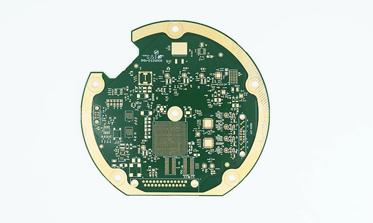
In PCB design, precision isn’t just a technical requirement—it’s central to achieving reliable performance. Especially in high-performance electronics, where factors like speed and signal clarity can’t be compromised, tightly controlled tolerances ensure every aspect of the board works as intended. When those tolerances slip, the results can be severe: degraded signal transmission, improper impedance matching, and a system that just doesn’t hold up under pressure. This section will dive into how fine-tuned tolerances influence things like signal integrity, impedance control, and crosstalk reduction, particularly in designs that push the envelope with high speeds and frequencies. Each millimeter and each calculation matters when every signal is expected to travel without error.
Signal Integrity and PCB Tolerances
Signal integrity (SI) is one of the biggest concerns in high-speed PCB designs, especially when circuits need to handle large amounts of data at lightning-fast speeds. Tight tolerances ensure that the traces, pads, and vias on a PCB are perfectly aligned and sized, avoiding any issues that could cause signal distortion.
●Trace Width and Length Consistency: A tiny change in the width or length of a signal trace can result in impedance mismatch, leading to signal reflections, attenuation, or even complete signal loss. Maintaining tight tolerances means that the signal trace’s impedance stays consistent across the entire length, ensuring that signals travel with minimal interference or degradation.
●Via and Hole Placement: Any misalignment in vias or holes could lead to changes in the electrical characteristics of the PCB, such as increased inductance or capacitance, which can severely affect signal performance. By adhering to tight tolerances, these issues are avoided, ensuring clean signal flow.
●Noise Reduction: The precision in the PCB’s construction ensures that sensitive signal paths are separated from noisy power or ground layers, which is crucial for avoiding signal interference. In high-frequency designs, even the slightest noise can cause data errors or system malfunction.
Table: Impact of Tight Tolerances on Signal Integrity-
| Tolerance Type | Potential Signal Integrity Issue | Effect on Performance | Example Application |
| Trace Width & Length | Impedance mismatch, signal reflections, attenuation | Reduced signal quality, errors, data loss | High-speed data transfer, RF designs, server boards |
| Via & Hole Alignment | Inductance and capacitance changes, signal distortion | Increased signal delay and reduced accuracy | High-performance processors, memory modules |
| Noise Isolation | Signal interference, crosstalk | Unreliable signal transmission, errors in high-frequency circuits | Communication equipment, 5G technology, aerospace |
Impedance Control in High-Performance PCB Designs
For high-frequency applications like RF circuits and telecommunications, managing impedance in PCB design ensures that signals pass through the traces smoothly, without interference or data loss. When impedance isn’t kept in check, problems like signal reflection and data corruption can arise. By adhering to tight tolerances, the design keeps impedance steady, supporting stable performance even at high speeds. This precision helps avoid issues with signal degradation or errors in data transmission, especially when the design pushes the limits of high-speed performance.
●Microstrip and Stripline Designs: In designs where traces are routed on the surface or embedded within layers (microstrip or stripline), the impedance is heavily influenced by the width of the trace and the spacing between layers. Even small deviations in these parameters can lead to impedance mismatches that result in signal reflections, signal loss, or data errors.
●Differential Pair Routing: For high-speed differential signals, such as USB or Ethernet, the relative impedance between the two traces in a pair must be tightly controlled. A variation in trace width or spacing can lead to skew or timing errors, significantly impacting the performance of the entire system.
●Use of Simulation Tools: We often use simulation tools to model impedance control, predicting how trace geometry and material properties will impact impedance. These simulations help ensure that designs stay within the acceptable tolerance range, avoiding any surprises during the manufacturing phase.
Impact of Tight Tolerances on Impedance Control-
| Tolerance Factor | Potential Issue | Effect on Impedance | Impact on High-Speed Systems |
| Trace Width & Spacing | Impedance mismatch, reflection, signal loss | Variations in signal impedance, affecting signal strength | Data transmission errors, signal integrity loss |
| Layer Stackup & Material | Changes in dielectric properties and trace geometry | Deviation from designed impedance, timing issues | High-frequency designs, RF applications |
| Differential Pair Spacing | Skewed signal timing, jitter | Incorrect impedance balance between differential pairs | Communication standards like USB, Ethernet, HDMI |
Reducing Crosstalk Through Precise PCB Tolerances
Crosstalk, or the unwanted coupling of signals between adjacent traces, is a common issue in complex PCB designs, especially when the circuits carry high-frequency signals. Maintaining tight PCB tolerances helps prevent crosstalk, which could otherwise lead to signal degradation, noise, and potential system failures.
●Trace Separation: When traces carrying high-speed signals are too close together, crosstalk can occur, where one signal “bleeds” into another. By carefully controlling the trace spacing through tight tolerances, we can reduce this unwanted interference, ensuring that each signal path remains isolated.
●Layer Isolation: Using a multi-layer PCB design can help reduce crosstalk by ensuring that sensitive signals are placed on layers that are physically separated from high-voltage or noisy layers. Tight tolerances help maintain the proper layer alignment, keeping crosstalk to a minimum.
●Use of Ground Planes: A well-placed ground plane between signal traces can act as a shield, helping to reduce crosstalk. Tight tolerances ensure that the ground plane is continuous and doesn’t have gaps that could lead to unwanted signal coupling.
Impact of Tight Tolerances on Crosstalk Reduction-
| Tolerance Factor | Potential Crosstalk Issue | Effect on Signal Integrity | Example Application |
| Trace Separation | Unwanted signal coupling between adjacent traces | Signal degradation, noise, interference | High-speed digital circuits, RF systems |
| Layer Alignment | Misalignment of signal and ground layers | Increased crosstalk between layers | Multi-layer PCBs, high-performance computing |
| Ground Plane Integrity | Gaps or interruptions in the ground plane | Increased susceptibility to crosstalk and noise | Communication devices, precision instrumentation |
Cost Implications of Tight PCB Tolerances
Achieving high precision in PCB manufacturing isn’t just a technical challenge; it has significant cost implications. While tight PCB tolerances are necessary for ensuring performance and reliability in demanding applications, they also come with a price tag. The key is to strike a balance between precision and cost-efficiency, ensuring that the product remains competitive while still meeting the required quality standards. Let’s explore how tighter tolerances influence costs, and how we can optimize their processes to achieve high-precision PCBs without breaking the bank.
Balancing Tolerance Precision with Production Costs
As PCBs become more intricate and the demand for high-performance electronics grows, the need for tighter tolerances increases. However, this level of precision often means higher costs, driven by several factors.
1.Increased Manufacturing Time: Achieving tight tolerances requires more meticulous work during the fabrication process. For example, controlling the dimensions of holes, trace widths, and spacing can take longer, as the machinery and processes need to be more accurate. The more time spent, the higher the labor costs and equipment usage costs.
2.More Expensive Materials: Certain high-precision applications may require specialty materials or high-quality substrates, which often come at a higher price. Materials such as Teflon, ceramics, or high-frequency laminates are more expensive than standard FR4 substrates, adding to the overall cost.
3.Higher Scrap Rates: Tight tolerances increase the risk of defects. If a PCB doesn’t meet the tolerance requirements during production, it needs to be scrapped or reworked, raising material and labor costs. This is particularly true for multi-layer PCBs, where the risk of defects multiplies with each added layer.
4.Specialized Equipment: Achieving precise tolerances often requires state-of-the-art machinery, such as laser drilling machines, automated optical inspection systems, and high-precision etching machines. The upfront investment in these tools can be substantial and contributes to higher production costs.
Strategies to Balance Precision and Cost-
Despite these added costs, there are strategies that can help balance the cost vs. quality equation:
●Design for Manufacturability (DFM): By designing PCBs that are optimized for production processes, we can reduce unnecessary complexity, which in turn reduces costs. This includes ensuring that trace widths and hole sizes align with the manufacturer’s capabilities.
●Batch Production: When manufacturers produce larger batches, the fixed costs of equipment setup and material procurement are spread across more units, reducing the per-unit cost.
●Supply Chain Optimization: By sourcing materials in bulk and working with trusted suppliers, manufacturers can reduce material costs without compromising quality.
Cost Implications of Tight PCB Tolerances-
| Tolerance Factor | Cost Impact | Possible Strategies to Offset Cost |
| Manufacturing Time | Longer production cycles lead to higher labor costs | Streamline design process, use batch production |
| Material Costs | Premium materials increase overall cost | Use standard materials where possible, bulk purchasing |
| Scrap Rates | Defects lead to wasted materials and labor | Improve quality control, reduce complexity |
| Specialized Equipment | Investment in advanced machinery increases setup costs | Invest in high-precision tools for larger batch runs |
Economical Solutions for Achieving Tight PCB Tolerances
While achieving tight tolerances can be costly, there are ways to optimize the manufacturing process to reduce overall expenses without sacrificing quality. we have developed several cost-effective solutions for producing high-precision PCBs:
1.Standardizing Tolerances: For many products, not every feature needs to be manufactured to the highest precision. By analyzing the design and focusing on areas that require tight tolerances, we can reduce unnecessary costs in less critical sections of the board. For instance, via holes may not need to be as precise as signal traces or component pads.
2.Use of Automated Inspection Tools: Advanced automated inspection systems help us quickly detect defects and ensure compliance with tolerance specifications. These tools can minimize the need for manual inspections, reducing labor costs and the potential for human error.
3.Optimizing Manufacturing Processes: Processes such as laser drilling and automated routing can be adjusted to improve efficiency, making it easier to meet tight tolerances without driving up costs. Optimizing the layer count for multi-layer boards can also significantly reduce the manufacturing complexity and associated costs.
4.Outsourcing: In some cases, it may be more cost-effective to outsource the manufacturing to specialized vendors who have already optimized their processes for tight tolerances. Global supply chains can be leveraged to find the best balance of cost and precision.
Economical Solutions for Tight Tolerances-
| Solution | Cost Reduction Impact | Example Application |
| Standardizing Tolerances | Reduce costs by focusing precision only where necessary | Non-critical vias, general trace routing |
| Automated Inspection Systems | Decrease manual inspection time and error rates | Visual inspection in complex high-density boards |
| Optimizing Manufacturing Processes | Streamline operations, reduce equipment wear and tear | Laser etching, automated drilling |
| Outsourcing | Benefit from vendor economies of scale | Outsourcing to specialized PCB manufacturers |
Scaling Manufacturing While Maintaining Tolerance Precision
As the demand for high-precision PCBs increases, we face the challenge of scaling production while maintaining tight tolerances. Mass production of PCBs is tricky because maintaining high tolerance standards across thousands or millions of units is difficult.
1.Automation: One of the best ways to scale production while ensuring that tight tolerances are met is by incorporating more automation into the manufacturing process. Automated PCB inspection, automated component placement, and automated soldering systems can help ensure that each PCB is manufactured with precision, regardless of scale.
2.Modular Production Lines: we can build modular production lines that allow us to scale up quickly while ensuring that all units are produced under the same conditions. This approach helps maintain consistent tolerance levels and reduces the potential for errors when switching between production runs.
3.Quality Control Systems: Tight tolerance specifications require continuous quality monitoring. Implementing real-time quality control systems that track every phase of the production process helps identify issues before they escalate, preventing costly rework and defects in large production batches.
4.Supplier Partnerships: Building long-term relationships with suppliers that specialize in high-precision components allows us to access cost-effective materials while maintaining high-quality standards.
Scaling Manufacturing with Tight Tolerances-
| Strategy | Benefit | Example Application |
| Automation | Increases throughput while maintaining consistent quality | Automated assembly, automated optical inspection |
| Modular Production Lines | Flexible scaling with minimal compromise on precision | Mass production of consumer electronics, medical devices |
| Quality Control Systems | Early detection of defects reduces waste and improves yield | Continuous monitoring during PCB fabrication |
| Supplier Partnerships | Access to high-precision components at scale | Long-term agreements with high-precision PCB suppliers |
Why Choose Us Manufacturing your PCB Circuits Board?
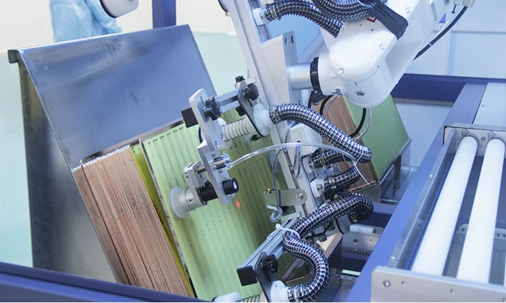
Each PCB manufacturer has its own tolerances for PCBs that impact the engineer’s goal in determining the impedance as well as a pile-up. While it is not required, however, it’s extremely helpful for the designer of the PCB to get in touch with a PCB fabricator as well as the PCB assembly company in the early stages during the layout and design process to obtain an accurate duplicate of PCB tolerance requirements as well as stack-up. One advantage of working with a company such as JarnisTech is that everything is handled in one place – design, Engineering consultations as well as fabrication, component procurement as well as assembly.
Our expertise is offering the best solution for the most difficult design issues and the most demanding of applications, whether that be critical reliability or high-heat standards. We offer these cutting-edge technologies to our customers, which are transforming the way you purchase printed circuit boards. Therefore, With us, clients there’s no longer a need to manage numerous supplier relationships and be accountable for miscommunications on issues such as the overage of components and tolerances.
Please find the following our PCB manufacturing capabilities tolerances:
1.Via (finished) Diameter Tolerances
| Via Type | Via Diameter | Tolerance |
| Plated Thru-hole (PTH) | ≤ 0.8mm | ± 0.08mm |
| > 0.8mm, < 2.5mm | ± 0.1mm | |
| > 2.5mm, ≤ 6.3mm | ± 0.15mm | |
| > 6.3mm | ± 0.2mm | |
| Non-Plated Thru-hole (NPTH) | ≤ 0.8mm, > 0.8mm, ≤ 6.3mm | ± 0.05mm |
| > 6.3mm | ± 0.2mm | |
| Paper-based PCB | ≤ 0.8mm | ± 0.1mm |
| > 0.8mm | ± 0.2mm | |
| PTH Slots | < 10.0mm | ± 0.2mm |
| ≥ 10.0mm | ± 0.3mm | |
| NPTH Slots | < 10.0mm | ± 0.15mm |
| ≥ 10.0mm | ± 0.2mm |
2.Board-dimensional Tolerances
| Dimension | Range | Tolerance |
| Board Thickness (Finished) | ≤ 1.0mm | ± 0.10mm |
| ≤ 1.6mm, > 1.0mm | ± 0.14mm | |
| ≤ 2.0mm, > 1.6mm | ± 0.18mm | |
| ≤ 2.4mm, > 2.0mm | ± 0.22mm | |
| ≤ 3.0mm, > 2.4mm | ± 0.25mm | |
| > 3.0mm | ± 10% | |
| Lamination Thickness | / | ± 8% |
| Board Size (Finished) | / | ± 0.1mm – ± 0.3mm |
3.Mechanical Manufacturing Tolerances
| Item | Specific Aspect | Tolerance |
| Hole Location Tolerances | Drilling | ± 0.18mm |
| Milling | ± 0.15mm | |
| V-cut | V-cut Remain Thickness | ± 0.1mm |
| Bevelling | Bevelling Angle | ± 5° |
| Edge Milling | Ordinary Parts | ± 0.13mm – ± 0.4mm |
| Internal Slot | ± 0.20mm | |
| Card Slot | ± 0.15mm | |
| Countersink / Counterbore | Depth | ± 0.20mm |
| Angle | ± 5° |
Therefore, We a Top PCB Manufacurer in China, JarnisTech gives you up the guidelines for tolerances in-house to ensure quality production of printed circuit boards. Following these tolerances will ensure the proper manufacturing of PCBs. Within these parameters, there’s enough variance to allow us to make the board and allow it to function effectively in your application. Please contact us if you have any concerns or would like to discuss your unique needs.
FAQ & PCB Tolerance
How do PCB tolerances impact the choice of surface finish?
Surface finishes like ENIG ensure uniform flatness, while HASL may cause uneven surfaces, affecting tight tolerances.
What is the relationship between PCB copper weight and trace tolerance?
Heavier copper layers require wider trace spacing due to etching limitations, impacting precision in design.
How do PCB tolerances vary for flexible vs. rigid PCBs?
Flexible PCBs require strict bend radius control, while rigid PCBs focus on thickness and layer alignment.
Can tight PCB tolerances affect assembly processes like soldering or reflow?
Tight tolerances may lead to soldering issues, such as bridging or misalignment, managed through precise stencil design.
What is the impact of PCB tolerances on thermal dissipation?
Inconsistent copper thickness or board flatness can lead to uneven heat distribution, especially in power PCBs.
How do PCB tolerances affect component placement in automated assembly?
Accurate tolerances ensure proper alignment of components, reducing placement errors in high-speed assembly lines.
What role do tolerances play in HDI PCB designs?
HDI PCBs demand precise tolerances for microvias and fine traces, achieved through advanced laser and lamination processes.
Related Posts:
1.Why Aspect Ratio is So Important in PCB Design and Fabrication?

