
As artificial intelligence, 5G infrastructure, and hyperscale data centers demand ever-faster data transmission, optical modules have become the bedrock of modern communication. The Printed Circuit Board (PCB) at the heart of these modules is no longer a simple substrate but a highly engineered system. Designing and producing these complex PCBs presents formidable challenges, requiring a convergence of disciplines—from high-frequency signal integrity and advanced thermal management to micron-level mechanical precision.
This guide serves as an in-depth resource for engineers, designers, and project managers involved in the development of optical module PCBs. It will explore the complete product lifecycle, from design principles and advanced material selection to the intricacies of precision fabrication, electro-optical assembly, and quality validation. The document will delve into practical considerations such as cost optimization, lead time management, the specific requirements of various industry applications, and the value of collaborative engineering support.
Why Optical Module PCBs Are a Unique Engineering Challenge?
Unlike conventional PCBs, those designed for optical modules operate at the intersection of extreme electrical performance, stringent thermal constraints, and microscopic mechanical tolerances. The board itself is an active component in the system, and its design dictates the success or failure of the entire module.
●Extreme Data Rates: As data rates climb to 112 Gbps, 224 Gbps per lane, and higher—driven by advanced modulation schemes like PAM4—the PCB must serve as an almost invisible transmission path. Even the slightest variation in trace shape, material quality, or via design can distort the signal and result in bit error rates (BER) that exceed acceptable limits.
●Intense Thermal Loads: High-performance components like Digital Signal Processors (DSPs), drivers, and TIAs are densely packed, generating significant heat in a tiny, often enclosed, space. The PCB must not only withstand high temperatures but actively participate in the thermal dissipation strategy to prevent component throttling or premature failure.
●Mechanical Precision: The PCB serves as the mechanical foundation for optical sub-assemblies (TOSAs/ROSAs). It requires exceptional flatness and dimensional stability to ensure that lenses and fibers can be aligned with sub-micron accuracy. Any warpage or CTE (Coefficient of Thermal Expansion) mismatch can compromise this alignment.
●Miniaturization and Density: Form factors like QSFP-DD and OSFP demand immense functionality within a constrained footprint. This necessitates the use of advanced High-Density Interconnect (HDI) techniques, including stacked microvias and ultra-fine line/space features, pushing fabrication capabilities to their absolute limit.
Mastering these four interconnected challenges is the essence of creating a successful optical module PCB.
Optical Module PCB Applications and Form Factors
The design philosophy for an optical module PCB is fundamentally shaped by its end application. The performance benchmarks, reliability standards, and physical constraints are dictated by the operating environment.
Data Centers & High-Performance Computing (HPC)
Modern data centers and HPC clusters are built on the principles of maximum density and speed. They process immense volumes of internal traffic where minimal latency is a requirement. Transceivers like QSFP-DD and OSFP, supporting 400G, 800G, and 1.6T, are common in these environments.
●Engineering Focus: The primary objective is to maintain signal integrity. The PCB must function as a clean conduit for signals traveling at 112 Gbps PAM4 and higher.
| Parameter | Target Value / Technique |
| Data Rate | ≥112 Gbps PAM4 |
| Dielectric Loss (Df) | ≤0.002 (e.g., Megtron 7, Rogers 4350B) |
| Conductor Profile | VLP or HVLP copper foil |
| Impedance Tolerance | ±5% (typically 90Ω differential) |
| Thermal Solutions | Copper coins, thermal vias, optimized power planes |
1.Low-Loss Materials: The use of ultra-low-loss materials, like the Megtron or Rogers series, combined with very-low-profile (VLP) copper foils, serves to minimize both dielectric and conductor losses.
2.Impedance Control: Trace geometries are controlled with high precision (e.g., ±5% impedance tolerance) to prevent signal reflections that can degrade performance.
3.Thermal Engineering:The PCB layout incorporates thermal vias, embedded copper coins, and carefully planned power planes to efficiently draw heat away from power-hungry DSPs and towards the module’s heatsink.
●Form Factor Considerations:
1.QSFP-DD/OSFP: These pluggable modules need robust PCBs that withstand numerous insertion cycles. The designs leverage advanced HDI and back-drilling to manage the complex breakout from the high-pin-count edge connector, ensuring signal purity. The larger OSFP format allows for higher power delivery and integrated heatsinks, often necessitating localized heavy copper planes on the PCB.
2.Co-Packaged Optics (CPO): In this architecture, the optical engine is mounted on the same substrate as the switch ASIC. The “PCB” becomes a large, complex organic interposer. This design shortens electrical paths to reduce signal loss but introduces considerable manufacturing and assembly challenges, including co-designing electrical and photonic layers and achieving nanometer-level alignment accuracy.
5G Infrastructure & Telecom Networks
Unlike the controlled climate of a data center, telecom equipment faces the harshest environments. Systems deployed on cell towers or in street-side cabinets must operate flawlessly for decades, enduring extreme temperature swings, humidity, and mechanical vibration.
●Engineering Focus:Long-term operational reliability guides every design choice. PCBs must be built from materials with a high Glass Transition Temperature (Tg>170∘C) to resist warping or delamination during thermal cycling. In these mixed-signal boards, where high-power RF circuits operate alongside sensitive digital logic, preventing Electromagnetic Interference (EMI) is a priority. The layout must carefully isolate different domains to avoid crosstalk and maintain signal purity.
| Parameter | Typical Specification |
| Glass Transition Temp. | >170°C |
| Z-axis CTE | <3.0% (to prevent via fatigue) |
| EMI Mitigation | Guard traces, stitched GND planes, internal shields |
| Conformal Coating | IPC-CC-830B / MIL-I-46058C compliant |
| Operating Temperature | -40°C to +85°C (or wider for outdoor telecom) |
1.High-Tg Materials: Fabrication PCBs from materials with a high Glass Transition Temperature (Tg>170∘C) and a low Z-axis CTE to resist warping and prevent via fatigue failures during repeated thermal cycling.
2.EMI Shielding: These are often mixed-signal boards where high-power RF amplifiers operate alongside sensitive digital logic. The layout must be meticulously planned to isolate different domains using guard traces, ground planes, and internal shielding layers to prevent crosstalk and ensure electromagnetic compatibility (EMC).
3.Conformal Coating: To protect against moisture and contaminants, PCB manufacturer apply specialized conformal coatings that meet stringent industry standards, ensuring the board’s integrity over its service life.
●Form Factor Considerations:
1.SFP/SFP28/SFP56: Used at the network edge, these compact modules demand exceptional miniaturization in the PCB design. Trace routing and component spacing are tightly constrained, and the assembly process requires high-precision SMT placement to integrate all functions within the small footprint.
2.CFP/CFP2: Found in core network routers and DWDM systems, these larger modules feature longer PCBs. The design challenge here is maintaining signal integrity over extended trace lengths while managing the significant power drawn by long-haul optical components like cooled lasers.
Medical Imaging & Biomedical Instruments
In the medical field, precision, safety, and cleanliness are absolute requirements. Devices such as Optical Coherence Tomography (OCT) scanners and photonic biosensors depend on custom optical modules where the PCB serves as a stable mechanical and electrical foundation.
●Engineering Focus: Material purity and process control are foundational.
| Attribute | Specification or Method |
| Cleanroom Level | ISO Class 7 or better |
| Material Outgassing | <1% TML (per ASTM E595) |
| Biocompatibility | ISO 10993 or USP Class VI compliant materials |
| Regulatory Standard | IEC 60601-1 (for safety, spacing, and insulation) |
| Surface Finish | ENIG or ENEPIG (for wire bonding & cleanliness) |
1.Cleanliness & Biocompatibility: Fabrication and assembly often occur in certified cleanroom environments (e.g., ISO 7) to prevent particulate contamination. So selecting materials for their low-outgassing properties to avoid depositing residues on sensitive optics over the device’s lifetime.
2.Safety & Compliance: All designs must adhere to stringent medical safety standards like IEC 60601-1, which dictates choices for insulation, creepage, and clearance distances to protect both patients and operators.
●Form Factor Considerations:
1.Custom Shapes & Rigid-Flex: The PCBs for medical devices are nearly always custom-built to fit a specific optical bench or instrument housing. This can involve high-precision mechanical features, such as machined cavities with exceptionally flat surfaces for mounting lens assemblies, or rigid-flex designs that allow the circuit to conform to the irregular shapes of portable equipment.
Aerospace & Defense
Applications in aerospace and defense (A&D) push the boundaries of reliability. PCBs in avionics, satellite communications, and military-grade sensors must perform flawlessly under extreme g-forces, shock, vibration, and wide temperature ranges.
●Engineering Focus: Uncompromising robustness and traceability are non-negotiable.
| Feature | Standard or Technique |
| Reliability Class | IPC-6012 Class 3/3A |
| Shock/Vibration Endurance | MIL-STD-810G compliant |
| Traceability | Full lot tracking and serialization |
| Component Mounting | Solder + epoxy staking or hardware reinforcement |
| Counterfeit Prevention | Procurement through traceable, authorized sources |
1.High-Reliability Standards: Manufacturing to high IPC standards (e.g., IPC-6012 Class 3/3A), where failure is not an option, includes stringent coupon testing and lot traceability.
2.Component Mounting: Heavy components are secured not just by solder but often with additional staking compounds or specialized mounting hardware to withstand extreme mechanical shock and vibration.
3.Counterfeit Prevention: Supply chain management follows strict procedures to guarantee that every component is genuine and obtained through authorized distributors—an absolute requirement in A&D applications.
●Form Factor Considerations:
1.Ruggedization: Form factors are often custom and built into ruggedized enclosures. The PCB design must account for chassis grounding, thermal transfer to the chassis, and robust connector interfaces designed for harsh environments. Rigid-flex is often employed to reduce weight and increase reliability in dynamic systems.
The Integrated Lifecycle: From Concept to Mass Production with JarnisTech
Creating a high-performance optical module is an interconnected process, not a linear sequence of hand-offs. A design choice made in the first hour can directly impact fabrication yield and assembly reliability weeks later. At JarnisTech, we’ve built our entire operation around this holistic philosophy. Our integrated, under-one-roof approach ensures every stage informs the others, transforming a functional prototype into a robust, mass-producible product.
Stage 1: Collaborative Design & Strategic Simulation
The journey begins with a blueprint engineered for performance and manufacturability. This foundational stage is a delicate balance of physical layout, electrical modeling, and material science.
●Design for Manufacturability (DFM) Review: The process can begin with a collaborative DFM review. Engineers analyze the design files, identifying subtle issues—from via-in-pad reliability risks to soldermask clearances impacting high-speed signals—and provide actionable feedback to improve yields and reduce costs.
●Stack-Up & Material Strategy: The stack-up is the board’s architectural plan. It is designed to actively manage signal behavior, often using hybrid constructions that place high-performance, low-loss materials only where needed, balancing performance and cost. High-Tg materials are selected to ensure stability during high-temperature assembly.
●Predictive Signal Integrity Modeling: Before fabrication, the design is tested in a virtual environment. Using simulation tools, the entire signal path is modeled to optimize for impedance consistency, minimize signal loss (IL/RL), and reduce timing variations (jitter/skew). This predictive analysis helps ensure the design is robust before the first piece of copper is etched.
Stage 2: Precision Fabrication & In-Process Quality Control
This is where the simulated design is translated into a physical product with exacting precision. This stage demands deep fabrication expertise and microscopic process control.
●Advanced HDI & Fine-Line Processes: To accommodate the routing density, advanced HDI methods are utilized. This includes employing processes like mSAP (Modified Semi-Additive Process) for ultra-fine lines down to 25μm, creating perfectly filled and planarized Via-in-Pad structures to shorten signal paths, and using sequential lamination to build complex 3D interconnects with stacked microvias.
●Laser Drilling & Back Drilling: CO2 and UV lasers are used to achieve precise microvia drilling down to 75 μm. For high-speed through-holes, controlled-depth back drilling is applied to selectively remove the unused via stub, which might otherwise behave like an antenna and significantly impact signal integrity at frequencies exceeding 28 GHz.
●Bare-Board Electrical Validation: Before assembly, the bare board must precisely match its intended design. This involves performing Time Domain Reflectometer (TDR) measurements on test coupons to ensure trace impedance remains within strict tolerances (such as ±8%), along with complete netlist verification using flying probe testers to detect any shorts or opens.
Stage 3: High-Accuracy Assembly & Opto-Electronic Integration
This final stage transforms the bare board into a fully functional optical module. It is a delicate process where mechanical precision and thermal management are necessary.
●High-Accuracy SMT Placement: State-of-the-art SMT lines are equipped with machine-vision-guided systems that achieve placement accuracy below 0.1 mm. This level of precision is necessary for mounting large, fine-pitch DSPs and for correctly aligning passive components and optical sub-assemblies (TOSAs/ROSAs).
●Controlled Reflow Soldering: The assembly process often involves multiple high-temperature reflow cycles. By using high-Tg materials selected during the design phase, the board remains dimensionally stable, protecting sensitive components and plated-through-hole integrity.
●Advanced Optical Alignment: For maximum performance, advanced active alignment techniques may be utilized, where optical components are positioned while powered on to achieve optimal light throughput.
Stage 4: Rigorous Validation & Reliability Assurance
A commitment to quality is demonstrated by measurement. A multi-layered validation process is the final arbiter of performance, ensuring every interconnect, signal path, and optical interface functions precisely to specification. This disciplined approach provides the traceability and assurance required for deployment in any system.
●Assembled Performance Validation: Once assembled, the module’s real-world optical performance is validated. Transmitter output power and receiver sensitivity are measured to confirm the module meets its link budget requirements. An Optical Time-Domain Reflectometer (OTDR) can be used to analyze internal reflections that could destabilize performance.
●Structural and Thermal Reliability Testing: Beyond verifying initial functionality, PCBs are engineered to withstand demanding tests such as Thermal Cycling (-40°C to +85°C) and accelerated Thermal Shock. These evaluations help ensure long-term reliability of all solder joints and vias.
●Compliance to International Standards: Our processes and products conform to globally recognized standards. We manufacture to IPC-6012 Class 3/3A for high-reliability applications, are fully compliant with environmental regulations like RoHS and REACH, and design with the principles of Telcordia GR-468 in mind, ensuring our boards withstand the stresses of their intended service environment.
Mastering the Core Challenges of Optical Module PCBs
True expertise lies in mastering the fundamental physics of the PCB. Below, we delve into three core areas where our engineering depth provides a decisive advantage for our clients.
Advanced Material Selection: The Foundation of Performance
The choice of laminate material is arguably the single most important decision in high-speed PCB design. It impacts everything from signal loss and impedance control to reliability and cost.
●Ultra-Low-Loss Laminates:For 112G+ applications, standard FR-4 does not meet performance requirements. A range of advanced materials is used, including options from Isola (Tachyon, I-Tera MT40), Panasonic (Megtron family), and Rogers (RO4000 series). Material selection is guided by the Dielectric Constant (Dk) and Dissipation Factor (Df) at the target operating frequency to ensure optimal signal integrity.
●Copper Foil Selection: At high frequencies, the signal travels on the surface of the copper due to the skin effect. A rough copper surface increases the path length and signal loss. The use of Very-Low-Profile (VLP) and Ultra-Low-Profile (ULP) copper foils can minimize this effect and improve performance.
●Hybrid Stack-ups: To manage cost, it’s not always necessary to build the entire board from the most expensive material. Designs can feature hybrid stack-ups, where low-loss materials are used for the high-speed signal layers, while other layers use more standard materials.. This requires expert control over the lamination process to manage the different CTE properties of the bonded materials.
| Material Type | Dk (10 GHz) | Df (10 GHz) | Tg (°C) | Notes |
| FR-4 (Standard) | 4.5 | 0.020–0.025 | ~135 | Inadequate for >28G |
| Megtron 6 | 3.5 | 0.002 | >180 | Excellent for 56G+ |
| I-Tera MT40 | 3.45 | 0.0035 | 200 | Cost-effective for mid to high speed |
| Rogers RO4350B | 3.48 | 0.0037 | >280 | Superior thermal stability |
| VLP/ULP Copper (μm) | – | – | – | 1–3 μm roughness, improves SI/IL |
Signal and Power Integrity (SI/PI): The Science of High-Speed Design
At data rates exceeding 50 Gbps, traces no longer behave as simple wires but as complex transmission lines.
●Mastering Impedance:2D field solvers are employed to accurately model trace geometries—including width, spacing, and height above the reference plane—in order to achieve tightly controlled target differential impedances (such as 90Ω or 100Ω). This modeling incorporates the specific resin content and pressed thickness of each layer for precise results.
●Controlling Crosstalk: The spacing between differential pairs and from other signals is meticulously managed to minimize crosstalk. Layout guidelines include recommendations for optimizing routing channels, implementing effective ground shielding, and maintaining adequate separation from high-noise signal paths.
●Power Distribution Network (PDN) Design: A stable power supply is fundamental to a module’s performance. The PDN is designed for low impedance across a wide frequency range to supply stable voltage to noise-sensitive components like DSPs and SerDes. This involves strategic placement of decoupling capacitors, use of solid power planes, and ensuring low-inductance return paths. Post-assembly, PDN impedance validation can be performed to ensure real-world performance matches the simulation.
| Parameter | Target / Spec |
| Differential Impedance | 90Ω / 100Ω ±5% (dependent on protocol) |
| Crosstalk Isolation (FEXT/NEXT) | -30 dB or better @ Nyquist frequency |
| PDN Impedance (Z_target) | <50 mΩ up to 1 GHz (typical) |
| Decoupling Cap Placement | Within 1–2 mm of critical IC power pins |
| Power Plane Ripple Target | <5% of nominal voltage |
Thermal Management: A Comprehensive Strategy for Heat Dissipation
With power densities in optical modules continuing to rise, an effective thermal strategy contributes to performance and reliability. The PCB is a part of this strategy.
●Thermal Vias: A common technique is placing an array of thermal vias directly under heat-generating components. These vias act as conduits, efficiently transferring heat from the top of the board to internal ground or power planes, or to the bottom side where it can be dissipated by a heatsink.
●Embedded Copper Coins: For components with extremely high thermal loads, solid copper coins can be embedded directly into the PCB. The component is mounted on the coin, creating a direct, low-resistance thermal path to a heatsink. This technique is effective but requires advanced fabrication processes to ensure a reliable, co-planar result.
●Vapor Chambers & Heat Spreaders: During assembly, advanced cooling structures are integrated with precision. This includes the careful application of Thermal Interface Materials (TIMs) to eliminate air gaps and enhance heat transfer, along with the installation of components such as vapor chambers that leverage phase-change mechanisms to rapidly distribute heat across a broader surface area.
| Cooling Method | Thermal Resistance (°C/W) | Common Application |
| Thermal Vias | ~1.5–3.5 (depending on density) | Under DSPs, FPGAs |
| Copper Coins (Embedded) | <1.0 | High-power ASICs, laser drivers |
| Vapor Chambers | <0.2 | Modules exceeding 15–20W |
| TIMs (e.g., gap fillers) | 0.5–5 W/m·K (conductivity) | Applied between chip and spreader/heatsink |
Advanced PCB Surface Finishes for Optical Modules
The surface finish on an optical module PCB is an interface that impacts signal integrity, assembly yield, and long-term reliability. Choosing the correct finish is an engineering decision that balances performance, cost, and application-specific demands.
ENEPIG (Electroless Nickel, Electroless Palladium, Immersion Gold): The Premier Choice
●Performance: Often called the “universal finish,” ENEPIG offers the highest level of reliability. The palladium layer acts as a robust diffusion barrier, preventing the underlying nickel from migrating into the gold layer. This completely mitigates the risk of “black pad” syndrome, a brittle intermetallic formation that can plague ENIG finishes and lead to field failures. For high-frequency signals, the smooth, dense surface provides excellent performance.
●Applications: It is a suitable choice for applications requiring gold wire bonding and offers exceptional solder joint strength for fine-pitch BGAs. Its chemical stability makes it suitable for multiple high-temperature reflow cycles. While it is a more expensive option, its reliability can be beneficial for certain systems in telecom, data centers, and A&D.
ENIG (Electroless Nickel, Immersion Gold): The Workhorse Finish
●Performance: ENIG has been the industry standard for many years due to its excellent flatness, good solderability, and suitability for fine-pitch components. The thin gold layer protects the underlying nickel from oxidation. However, the potential for phosphorous-rich nickel corrosion (black pad) during the immersion gold process, while significantly reduced with modern chemical controls, remains a non-zero risk.
●Applications: This option offers a balanced solution for a variety of applications where budget constraints exist but strong performance remains necessary. Due to the thin and specific characteristics of the immersion gold layer, it is typically not selected for use with gold wire bonding. Strict process control is applied throughout to ensure consistent, high-quality ENIG deposition.
Immersion Silver (ImAg): The High-Frequency Contender
●Performance: Immersion Silver offers the best performance for ultra-high-frequency signals. Unlike nickel-based finishes, silver has a conductivity very close to copper, and the “skin effect” at high frequencies is minimally impacted. It provides a very flat, solderable surface. Its primary drawback is susceptibility to tarnishing and creep corrosion when exposed to sulfur and humidity, requiring careful handling and storage in controlled environments.
●Applications: Ideal for RF and millimeter-wave applications where minimizing signal loss is the absolute top priority. It is often used in test boards and reference designs. The assembly process must be swift after the packaging is opened to prevent surface degradation.
Immersion Tin (ImSn) and OSP (Organic Solderability Preservative)
●Performance: Both ImSn and OSP are lower-cost alternatives. ImSn provides a flat, solderable surface but is prone to forming tin whiskers over time, which poses a short-circuit risk. OSP is an ultra-thin organic coating that protects the copper before soldering but is consumed during the first reflow cycle, making it unsuitable for processes requiring multiple heat cycles or post-assembly probing.
●Applications: These finishes are generally not recommended for the high-reliability, high-performance demands of most optical modules. They may be considered for low-cost, disposable, or less critical applications where long-term reliability and high-frequency performance are not primary drivers.
Manufacturing Tolerances and Design for Assembly (DFA) for Optical Module PCBs
The flawless performance of an optical module depends on the precise execution of its design, with manufacturing tolerances controlled at the micron level. Designing with these tolerances in mind is fundamental to transforming a theoretical schematic into a reliable, high-yield product. A collaborative approach is used to align the design with advanced manufacturing capabilities for optimal results.
The Anatomy of Tolerance Control:
●Layer-to-Layer Registration: In a multi-layer HDI board, precise alignment between layers is necessary to maintain connection integrity. Misalignment can result in via “breakouts,” where the drill bit misses the center of the target pad, potentially affecting the reliability of the connection. Manufacturing processes are controlled to achieve registration tolerances that meet or exceed IPC Class 3 standards, supporting dependable vertical interconnect structures.
●Drilling Accuracy: High-precision mechanical drills handle through-holes, while advanced UV laser systems create microvias. Accurate drill positioning guarantees vias align exactly with their target pads, and strict diameter control promotes even plating and stable impedance.
●Trace and Space Definition: Replicating the exact trace widths and spacings from the design is fundamental to achieving impedance control. The use of mSAP and other advanced etching techniques enables ultra-fine line definition with minimal undercut, ensuring the final copper geometry closely matches the simulation model.
●Solder Mask Registration: The solder mask defines the solderable areas. Misregistration can lead to solder mask covering a portion of the pad (reducing the solderable area) or, conversely, leaving adjacent copper exposed, creating a risk of solder bridging between fine-pitch component pads. Automated optical alignment systems guarantee accurate solder mask placement.
| Manufacturing Metric | Typical Tolerance (μm) | IPC Class 3 Requirement |
| Layer-to-Layer Registration | ±25 μm | ≤ ±50 μm |
| Mechanical Drill Accuracy | ±30 μm | ≤ ±75 μm |
| Laser Drill Accuracy (UV) | ±15 μm | ≤ ±25 μm |
| Minimum Trace / Space (mSAP) | 35 μm / 35 μm | Varies by fab |
| Solder Mask Registration | ±25 μm | ≤ ±50 μm |
Designing for Assembly (DFA) – A Collaborative Effort:
●Via-in-Pad Protection: When using via-in-pad designs to save space, the via must be properly filled with epoxy and planarized (capped). This practice helps ensure these structures are robust and do not trap solder or outgas during reflow.
●Optimized Pad Geometries: Feedback on BGA and fine-pitch component land patterns can lead to slight modifications to improve solder paste deposition and reflow performance, resulting in higher assembly yields. Adding “teardrops” where traces meet pads can improve the mechanical robustness of the connection.
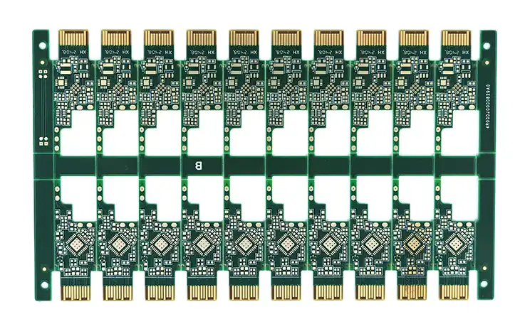
●Panelization Strategy: The arrangement of individual boards on a larger production panel affects both cost and quality. For delicate optical module PCBs, breakaway tabs (“mouse bites”) are often recommended instead of V-grooves to reduce stress on the board during de-paneling. In addition, some PCB manufacturers also work with you to design robust tooling strips on the panel for stable handling through the SMT line.
| DFA Design Element | Standard Practice or Value |
| Via-in-Pad Fill Type | Conductive/Non-Conductive Epoxy |
| Via Planarity Spec | ±10 μm |
| BGA Pad Size Tuning | Based on IPC-7351 / Fab feedback |
| Teardrop Radius | 0.25–0.5 mm typical |
| Panelization – Tab Width | 2–5 mm (mouse bite tabs) |
| Tooling Strip Width | ≥5 mm |
Advanced Quality Control and Testing Methodologies for High-Reliability Optical Modules
At JarnisTech, quality is not a department; it is a philosophy embedded in every step of our process. We believe that trust is earned through transparent, rigorous, and multi-layered validation. Our comprehensive quality control system ensures that every PCB we deliver is a perfect physical manifestation of its design, ready for core deployment.
In-Process Quality Gates:
●Incoming Material Verification (IQC): Quality starts with the raw materials. Every batch of laminate and copper foil is verified against its specification sheet for properties like thickness, dielectric constant, and copper weight before being accepted into production.
●Automated Optical Inspection (AOI): After the inner layers are etched, and again on the outer layers, 100% of the circuitry is scanned by high-resolution AOI systems. These systems compare the etched copper to the original Gerber data, flagging any potential defects like shorts, opens, or incorrect trace widths long before the layers are laminated.
Advanced Inspection and Validation Techniques:
●Automated X-Ray Inspection (AXI): For assembled boards with components like BGAs, where the solder joints are hidden underneath the package, AXI is indispensable. Both 2D and 3D AXI systems enable inspection through the component to detect shorts, opens, voids, and proper solder ball formation, confirming the integrity of these important connections.
●Microsection Analysis (Cross-Sectioning): This is a powerful destructive test performed on representative coupons from every production panel. A technician cuts through a plated hole or microvia, mounts it in epoxy, and polishes it. Under a high-magnification microscope, the technician measures copper plating thickness, checks for layer-to-layer registration, and inspects for any lamination defects. This provides direct, physical evidence of process quality.
Comprehensive Electrical and Performance Testing:
●Bare Board Testing: Beyond a basic continuity check, flying probe and bed-of-nails testers carry out 100% netlist verification to detect shorts and opens. High Potential (Hi-Pot) tests are also performed, applying high voltage between isolated conductors to confirm the dielectric strength of the insulation material, helping to ensure long-term resistance to electrical breakdown.
●High-Frequency Performance Verification: For 56G+ designs, reliance on simulation alone is avoided. A Vector Network Analyzer (VNA) is used to measure the board’s S-parameters (Scattering parameters). This process includes capturing the actual Insertion Loss (S21) and Return Loss (S11) of critical channels, delivering real-world data that confirms the signal integrity performance of the finished product.
Specific Challenges of Rigid-Flex PCBs in Optical Systems
Rigid-flex PCBs offer elegant solutions for creating compact, reliable 3D interconnects in optical modules, but their design and fabrication present a unique set of challenges that demand specialized expertise. Success with rigid-flex technology requires a deep understanding of the interplay between materials, mechanics, and electronics.
Material and Stack-up Complexity:
●CTE Mismatch: A core technical problem lies in laminating materials with vastly different properties. The polyimide used in flexible sections expands and contracts with temperature at a different rate than the FR-4 in the rigid sections. Managing this Coefficient of Thermal Expansion (CTE) mismatch during lamination affects board warpage and internal stress.
●Adhesive vs. Adhesiveless Cores: A designer must choose between traditional adhesive-based flex cores and modern adhesiveless cores. Adhesiveless cores, where the copper is bonded directly to the polyimide, offer superior thermal stability and thinner constructions, making them preferable for high-performance optical applications.
| Property | FR-4 (Rigid) | Polyimide (Flex) | Adhesive-Based Flex | Adhesiveless Flex |
| CTE (Z-Axis, ppm/°C) | 50–70 | 20–30 | 35–45 | 18–22 |
| Thermal Stability (Max °C) | 130–150 | ≥200 | ~180 | ≥250 |
| Thickness per Layer (μm) | ~150 | ~25–50 | ~75–100 | ~50–70 |
| Dielectric Constant (Dk @1GHz) | 4.2–4.5 | 3.2–3.5 | 3.5–3.8 | 3.2–3.4 |
| Preferred Use Case | Rigid sections | Flex/bend areas | Moderate flex use | High-performance, HDI flex |
Designing for Mechanical Reliability:
●The Transition Zone: The area where the circuit board transitions from rigid to flexible is a point of high mechanical stress. Designs must incorporate gradual, smooth transitions. Traces should cross the transition zone at a 90-degree angle to the bend line to minimize stress on the copper. Sharp corners in the outline or traces must be avoided in this area.
●Bend Radius and Routing: Each flex section has a minimum bend radius determined by its thickness and material makeup. Bending tighter than this radius risks damaging the copper traces. It is recommended to route traces in a single layer within the bend area when possible and to use cross-hatched ground planes rather than solid ones to enhance flexibility.
Fabrication and Assembly Nuances:
●Stiffeners and Reinforcements: Many rigid-flex designs require stiffeners (typically made of FR-4 or metal) to be bonded to the flex sections. These are used to support the weight of components or to create a solid, flat area for ZIF (Zero Insertion Force) connectors. The precise placement and bonding of these stiffeners are main assembly steps.
●Coverlays vs. Solder Mask: Flexible sections are protected by a flexible coverlay film, not a liquid photoimageable (LPI) solder mask. The coverlay openings must be precisely defined to expose the solder pads. The entire assembly process requires specialized fixtures and handling protocols to support the flexible parts of the board during SMT placement and reflow.
| Assembly Feature | Standard Specification | Function & Importance |
| Stiffener Material | FR-4, PI, or stainless steel | Adds rigidity for connector or component support |
| Stiffener Thickness | 0.15 mm – 1.5 mm | Depends on application (ZIF vs. general SMT) |
| Coverlay Opening Accuracy | ±50 μm typical | Ensures clean pad exposure for soldering |
| Coverlay Thickness | 25–50 μm | Thinner than LPI solder mask; maintains flexibility |
| Handling Fixture Requirement | Mandatory during reflow | Prevents flex section distortion or tearing |
The Future of the Optical Module PCB: CPO and Next-Generation Substrates
The evolution of optical interconnects is relentless. As pluggable modules approach the physical and thermal limits of copper-based PCBs, the industry is transitioning to a new era of deeper integration where the lines between silicon, photonics, and circuit boards blur.
●The Shift to Co-Packaged Optics (CPO): The future lies in bringing optics closer to the processing chip. CPO, enabled by Silicon Photonics (SiPh), achieves this by placing optical engines directly on the same package substrate as the main switch ASIC. This shortens high-speed electrical paths from centimeters to millimeters, dramatically reducing power consumption per bit and enabling unprecedented bandwidth density.
●New Frontiers in Substrate Fabrication: CPO demands a quantum leap in substrate complexity, far beyond conventional PCB capabilities. This includes line/space features approaching semiconductor levels (e.g., sub-10μm) and managing the significant warpage and CTE mismatch between large organic substrates and silicon dies. Mastering these challenges through advanced materials and Semi-Additive Processes (SAP) is fundamental to the CPO revolution.
●Ultra-Precision Assembly & Optical Coupling: Connecting SiPh chiplets to fiber arrays requires alignment with sub-micron precision—a task impossible for standard SMT equipment. This new reality depends on specialized automated systems that perform active alignment (optimizing light transfer while the device is powered on) and a substrate fabricated with extreme surface flatness to facilitate it.
●Your Partner for the Next Generation: Navigating this transition from board-level to package-level integration requires a partner with deep, cross-disciplinary expertise. JarnisTech is actively developing the process controls and capabilities to solve these next-generation challenges, ensuring we remain your trusted partner in an integrated future.
Your Engineering Partner: Why JarnisTech’s Integrated Approach Matters?
Developing next-generation optical modules requires more than a supplier; it demands a true engineering partner. At JarnisTech, we’ve built our entire process around this principle, providing a seamless, accountable partnership from concept to mass production.
Unmatched Expertise Under One Roof
We manage the entire critical path—from collaborative DFM and fabrication to final assembly and testing—in-house. This integrated model is our core strategic advantage, and it becomes yours.
●Accelerated Development Cycles: By eliminating the communication gaps and logistical delays between separate fab and assembly houses, we significantly shorten your time-to-market.
●Holistic Problem Solving: When a challenge arises, there is no finger-pointing. Our fabrication, assembly, and testing engineers work together in the same facility to diagnose and solve the root cause, whether it’s a design flaw, a process issue, or a material incompatibility.
●Single Point of Accountability: You have a single, dedicated partner responsible for the quality, delivery, and performance of your final product. This simplifies your supply chain and gives you peace of mind.
Optimizing for Cost, Lead Time, and Performance
We understand that technical excellence must align with business reality. Our collaborative approach makes the trade-offs between cost, speed, and performance transparent.
| Optimization Focus | Strategy Employed | Client Benefit |
| Material Stack-Up | Use hybrid stack-ups (e.g., Megtron + FR-4) | Performance where needed, reduced total cost |
| Cost Transparency | Real-time cost modeling based on stack-up | Informed engineering trade-offs |
| Trace Width vs. Yield | Data on yields vs. <50μm traces provided | Avoid over-specification; protect budget |
| Timeline Predictability | Integrated scheduling of fab + assembly | Reliable go-to-market planning |
| Capacity Planning | Clear lead times by stage (see below) | Reduced supply chain risk |
●Material & Stack-Up Strategy: We help you navigate the cost of high-performance laminates by exploring qualified material alternatives or designing intelligent hybrid stack-ups that deliver performance where it’s needed most.
●Predictable Timelines: Our integrated process offers clear, reliable scheduling.
1.Prototypes (Complex HDI): 7–12 working days
2.Pilot Batches (with SMT Assembly): An additional 3–5 days
3.Mass Production: 2–4 weeks after process stabilization
●Data-Driven Decisions: Requirements for ultra-fine traces (<50μm) or exceptionally tight tolerances influence cost. We provide clear data on these trade-offs, helping you make informed decisions that meet both your performance goals and your budget.
Let’s Engineer Your Next-Generation Solution
Your optical module has unique demands. Our team is ready to understand them and build a PCB solution engineered for your specific application. We don’t just build boards; we build partnerships that power innovation.
Reach out today to start a technical conversation with one of our engineers and discover how our integrated approach can de-risk your project and accelerate your success.
FAQs about Optical Module PCB
1.What design files are required to start a project for an optical module PCB?
Required files: Gerber (RS-274X), Excellon drill, a stack-up diagram, Bill of Materials (BOM), and Pick-and-Place data for assembly.
2.Is rework or repair supported for PCBs with already assembled optical components?
Rework is extremely high-risk and not recommended due to high component density and the need for precise optical alignment. Damage to the board or adjacent components is likely.
3.What are the main advantages of using a rigid-flex PCB for an optical module application?
Key advantages include enabling compact 3D designs, improving signal integrity by eliminating connectors, and increasing reliability against vibration and shock.
4.Is it possible to perform laser trimming of passive components on an assembled optical module PCB?
Yes, on-board thin-film or thick-film resistors can be laser-trimmed post-assembly to precisely calibrate circuit parameters. The design must include a clear line of sight for the laser.
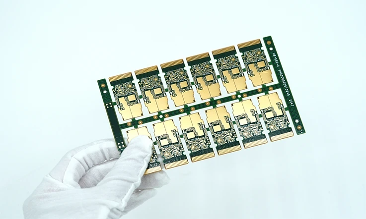
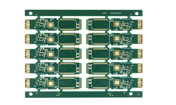
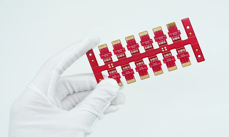
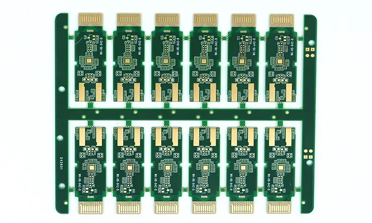
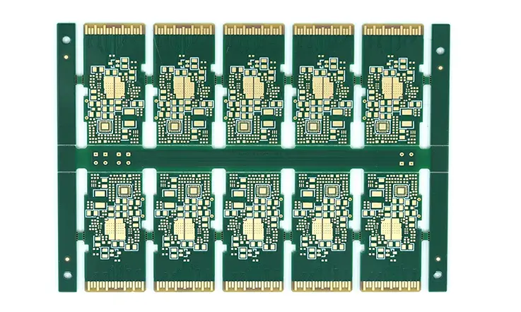
5.How are small optical module PCBs typically panelized for efficient SMT assembly?
Using V-grooves or breakaway tabs (“mouse bites”). Panels include tooling strips for machine handling and fiducial marks on both the panel and individual boards for precise component placement.