Introduction:
When designing a printed circuit board (PCB), the surface finish is often overlooked, yet it directly influences the board’s durability, solderability, and overall assembly process. As the final step in PCB manufacturing, surface finishes protect exposed copper from oxidation, enhance solder connections, and support the board’s long-term functionality under varying conditions.
In this article, we will explore the different surface finish methods used in PCB manufacturing, why they matter, and how to choose the best one for your project. From traditional finishes to cutting-edge technologies, we’ll break down each option, its advantages and disadvantages, and how they fit into various industrial applications.
The Evolution of PCB Surface Finishes: From Traditional to Advanced Methods
PCB surface finishes have evolved significantly over the years, driven by advances in technology, changes in manufacturing processes, and the increasing demand for more reliable, high-performance electronics. What was once a straightforward choice between a few basic finishes has now become a complex decision, with a range of options available. Let’s explore how these finishes have changed over time.
The Traditional Surface Finish Methods
For many decades, Hot Air Solder Leveling (HASL) was the dominant method for PCB surface finishing. The process involves applying a layer of molten solder to the PCB’s copper surface and then leveling it off using hot air, ensuring a smooth, flat finish. This finish was a preferred choice for a wide range of applications due to its low cost and reliable performance.
However, as environmental concerns regarding lead-based solder began to mount, industries demanded alternatives that complied with regulations such as RoHS (Restriction of Hazardous Substances). This shift has led to the rise of lead-free HASL, which, while offering a similar cost-effective solution, eliminates the harmful effects of lead.
Despite the introduction of newer methods, HASL continues to be a practical option for mass production, especially when the PCB design does not require fine-pitch components or high-frequency capabilities. Let’s take a closer look at how HASL has evolved and some of the typical applications:
| Surface Finish Method | Key Characteristics | Typical Applications | Limitations |
| HASL (Lead-Based) | Coated with solder, leveled with hot air | Standard consumer electronics, automotive | Lead contamination, poor for fine-pitch designs |
| Lead-Free HASL | Similar to HASL but uses lead-free solder | Consumer electronics, non-critical devices | Slightly higher cost, limited fine-pitch compatibility |
The Rise of Advanced surface Finishes
Immersion finishes revolutionized PCB manufacturing by introducing a highly uniform coating that provided better protection against oxidation and a more stable soldering surface. These finishes became particularly important as the demand for high-speed, high-density electronic devices grew. Let’s break down the four most commonly used types of immersion finishes and their applications.
1.Immersion Gold (ENIG)-
Immersion Gold (ENIG) involves the deposition of a layer of gold over a nickel layer, which is chemically applied to the PCB surface. It is a popular choice for high-end applications that require superior conductivity and oxidation resistance. ENIG is particularly effective in fine-pitch components and high-frequency applications, such as telecommunication devices, medical equipment, and computing hardware.
| Advantages | Limitations |
| Excellent conductivity and corrosion resistance | Expensive due to the cost of gold |
| Ideal for fine-pitch designs and small features | Risk of gold embrittlement in certain designs |
| High reliability in critical, high-speed applications | Complex and multi-step process |
2.Immersion Silver-
Immersion Silver is often used for low-cost applications that do not require the performance characteristics of ENIG. It provides a smooth finish and offers excellent solderability. Silver’s excellent electrical conductivity makes it an ideal choice for RF (radio-frequency) applications, as well as consumer electronics that require a relatively low-cost but reliable finish.
| Advantages | Limitations |
| Smooth and uniform finish for better solderability | Tendency to tarnish over time, especially in humid environments |
| Cost-effective compared to ENIG | Requires additional protection to prevent oxidation |
3.Immersion Tin-
Immersion Tin is a popular surface finish choice for PCBs used in consumer electronics and automotive applications where budget considerations take center stage and high-frequency performance isn’t a primary concern. This finish stands out for its affordability and strong soldering performance. On the flip side, it falls short in oxidation resistance compared to alternatives like gold or silver, which may limit its shelf life and reliability in more demanding environments.
| Advantages | Limitations |
| Low cost and easy solderability | Susceptible to oxidation, which may impact performance over time |
| Often used for single-sided PCBs and non-critical applications | Less reliable in harsh environments |
4.Immersion Nickel-
Immersion Nickel provides a nickel surface finish that can act as a foundation for other finishes, such as gold or palladium, and is commonly used as a base layer for immersion gold (ENIG). This finish offers good solderability, and reliability, and is often used in hybrid designs where durability is a primary concern.
| Advantages | Limitations |
| Provides a strong base for other finishes | Limited shelf life, can develop “black pad” issues |
| Ideal for hybrid finishes like ENIPIG | Can be more expensive due to multi-step process |
Additional other advanced PCB surface methond (Surface Finish):
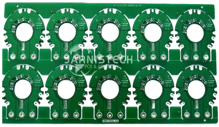
5.Gold Plating PCB Surface Finish-
Gold plating involves the application of a thin layer of gold over the surface of a PCB. This finish is particularly prized for its superior conductivity, corrosion resistance, and long-lasting performance.
Applications:
●High-end electronics: Often used in military, aerospace, and medical applications where performance and durability are non-negotiable.
●High-frequency designs: This finish is a go-to choice for components in data transmission and high-performance computing systems.
| Advantages | Limitations |
| Excellent for durability and conductivity | Higher cost compared to other finishes |
| Ideal for complex, high-frequency circuits | Requires specialized equipment and processes |
6.Nickel Plating PCB Surface Finish-
Nickel plating involves depositing a thin nickel layer over the PCB to improve its durability and resistance to wear. It is often used as a base for other finishes, such as gold plating.
Applications:
●Hybrid finishes: Nickel plating is often used as a base layer in multi-layer finishes, such as ENIPIG (Electroless Nickel Immersion Palladium Immersion Gold), which is seen in high-performance designs.
●Industrial applications: Used in automotive, aerospace, and industrial electronics where durability is key.
| Advantages | Limitations |
| Durable and wear-resistant | Typically needs a secondary finish (gold, palladium) |
| Ideal for heavy-duty designs | More expensive due to multi-step process |
7.Hard Gold PCB Surface Finish-
Hard Gold is used for high-wear applications due to its durability and high corrosion resistance. The gold layer is much thicker than flash gold and is often used in areas that require repeated electrical connections.
Applications:
●Connector pads: Commonly used in connector pads where frequent mechanical wear and tear occur.
●High-frequency electronic devices: Excellent for devices requiring consistent conductivity over time.
| Advantages | Limitations |
| Superior wear resistance | Expensive, due to thicker gold layer |
| Excellent for high-wear applications | Complex and expensive process |
8.Soft Gold PCB Surface Finish-
Soft Gold is often referred to as flash gold and is applied in a thin layer. It provides excellent solderability and conductivity but is not as durable as hard gold.
Applications:
●Fine-pitch PCB designs: Frequently used in fine-pitch components and applications where low wear is expected.
●Luxury consumer electronics: Used in high-end consumer devices such as premium smartphones or headphones.
| Advantages | Limitations |
| Provides excellent solderability | Not ideal for high-wear applications |
| More affordable than hard gold | Less durable than hard gold finishes |
9.Flash Gold PCB Surface Finish-
Flash Gold provides a very thin layer of gold for PCB surface finishing. It’s a cost-effective option for applications where only solderability and low-level performance are required.
Applications:
●Consumer-grade electronics: Often used in low-cost consumer products where solderability is the main concern.
●Prototyping and small-run production: Ideal for prototype boards or low-volume runs where cost is a main consideration.
| Advantages | Limitations |
| Cost-effective | Not durable for high-frequency or heavy-use environments |
| Good for basic electronic needs | Thin layer can result in reduced performance |
10.OSP PCB Surface Finish-
OSP is an organic-based layer that prevents oxidation on copper surfaces. It is applied through a chemical process, leaving a thin protective layer.
Advantages:
●Environmentally friendly and RoHS compliant.
●Inexpensive compared to other surface finishes.
Disadvantages:
●Limited storage life before oxidation sets in.
●Not suitable for high-temperature or high-humidity environments.
Applications:
●Used in consumer electronics, particularly where the PCB has a short lifespan or is shielded from environmental stresses.
OSP PCB Surface Finish Comparison
| Feature | OSP PCB Surface Finish |
| Conductivity | Moderate |
| Corrosion Resistance | Low |
| Thermal Stability | Low |
| Solderability | High |
| Durability | Low |
| Cost | Low |
| Typical Applications | Consumer Electronics |
12.ENEPIG PCB Surface Finish-
ENEPIG (Electroless Nickel Electroless Palladium Immersion Gold) is a multi-layer finish that combines the properties of nickel, palladium, and gold. It offers superior corrosion resistance and excellent solderability.
Advantages:
●Provides a highly durable and solderable surface.
●Extremely effective for fine-pitch components.
●Suitable for high-performance electronics requiring both electrical and mechanical reliability.
Disadvantages:
●More complex and costly process.
●Requires careful control to avoid issues in the gold immersion layer.
Applications:
Used in advanced electronic assemblies like medical devices, telecommunications, and high-frequency circuits.
ENEPIG PCB Surface Finish Comparison
| Feature | ENEPIG PCB Surface Finish |
| Conductivity | Very High |
| Corrosion Resistance | Very High |
| Thermal Stability | Very High |
| Solderability | Very High |
| Durability | Very High |
| Cost | High |
| Typical Applications | Medical Devices, Telecommunication |
Comparing PCB Surface Finish Methods: Performance and Cost
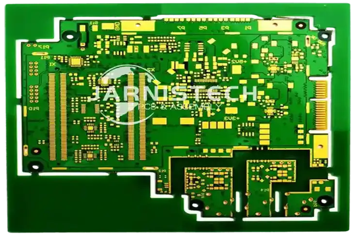
The surface finish you choose for your PCB influences its performance, longevity, and overall manufacturing cost. With 13 widely used surface finish methods available, each providing different benefits, it’s necessary to make an informed decision.. Below, we break down their material properties, cost implications, and best applications to guide you in selecting the optimal finish for your designs.
Material Properties Across 13 Surface Methods
Each surface finish varies in conductivity, thermal resistance, adhesion strength, and durability. The table below highlights these characteristics across 13 methods, helping you identify the best fit for your application:
Material Properties of 13 PCB Surface Finishes-
| Surface Finish | Conductivity | Thermal Resistance | Adhesion | Durability |
| HASL (Lead) | Good | Moderate | Standard | Moderate |
| Lead-Free HASL | Good | Moderate | Standard | Moderate |
| Immersion Gold (ENIG) | Excellent | Low | Superior for fine-pitch | High |
| Immersion Silver | Excellent | Low | Reliable | Moderate |
| Immersion Tin | Good | Low | Moderate | Moderate |
| Nickel Plating | Good | High | Excellent | High |
| Immersion Nickel | Moderate | High | Moderate | High |
| OSP (Organic Solderability) | Good | Low | Suitable for short-term | Low |
| Hard Gold | Excellent | High | Excellent | Very High |
| Soft Gold | Excellent | Moderate | Excellent | Moderate |
| Flash Gold | Excellent | Low | High | Moderate |
| ENEPIG | Excellent | Low | Superior | Very High |
| Gold Plating | Excellent | High | Excellent | High |
Cost Implications of Different PCB Surface Finishes
The cost of PCB surface finishes depends on material requirements and manufacturing complexity. Below is a breakdown of the financial aspects of all 13 methods:
Cost Overview of 13 PCB Surface Finishes-
| Finish | Material Cost | Processing Cost | Overall Cost Range |
| HASL (Lead) | Low | Low | $ |
| Lead-Free HASL | Low | Moderate | $ |
| Immersion Gold (ENIG) | High | High | $$$ |
| Immersion Silver | Moderate | Moderate | $$ |
| Immersion Tin | Moderate | Moderate | $$ |
| Nickel Plating | Moderate | High | $$ |
| Immersion Nickel | High | High | $$$ |
| OSP (Organic Solderability) | Very Low | Very Low | $ |
| Hard Gold | Very High | Very High | $$$$ |
| Soft Gold | High | High | $$$ |
| Flash Gold | Moderate | Moderate | $$ |
| ENEPIG | Very High | Very High | $$$$ |
| Gold Plating | High | High | $$$ |
Insights on Cost-
●Budget-Friendly Finishes: OSP, HASL, and Lead-Free HASL are ideal for cost-conscious designs.
●Premium Solutions: ENEPIG, Hard Gold, and Immersion Nickel target high-reliability applications where cost is secondary to performance.
●Balanced Choices: Immersion Silver and Immersion Tin strike a good balance between affordability and functionality.
Choosing the Right Surface Finish for Your PCB Design
The optimal surface finish depends on the application, environmental factors, and manufacturing priorities. Here’s a guide to help you navigate the decision:
Factors to Consider-
●Design Complexity: For intricate HDI designs, finishes like ENIG, ENEPIG, and Hard Gold ensure precise performance.
●Environmental Conditions: Products exposed to harsh environments, such as high humidity or extreme temperatures, benefit from durable options like Immersion Gold or ENEPIG.
●Lifecycle and Application: OSP is ideal for short-term applications, while Hard Gold is a favorite for wear-resistant needs like edge connectors.
●Budget Constraints: OSP and HASL are suitable for budget-sensitive projects, while ENEPIG and Hard Gold cater to high-end, high-reliability designs.
PCB Surface Finish for High-Density Interconnect (HDI) PCBs
High-Density Interconnect (HDI) PCBs are integral to the miniaturization and advancement of modern electronic devices. HDI technology allows for greater component density, faster performance, and reduced size—attributes crucial for devices such as smartphones, wearables, and automotive electronics. These designs demand precise manufacturing methods, particularly regarding PCB surface finishes. Surface finishes for HDI PCBs must be chosen with care to support the unique challenges that arise from these designs.
Why HDI Designs Require Specific Surface Methods?
The most significant challenge with HDI designs is the creation of smaller features, such as finer traces and microvias. These designs demand more precision in the PCB fabrication process, especially when it comes to the surface finish, as the finish must accommodate smaller components and tighter connections.
●Finer Traces: HDI boards use narrower trace widths to fit more components into a smaller area. This requires surface finishes that can handle these small, delicate traces without introducing resistance or reliability issues. Common finishes for this application include Immersion Gold (ENIG) and Immersion Silver. Both of these finishes offer fine, smooth surfaces that ensure minimal resistance and optimal signal flow across narrow traces.
●Microvias: The smaller via holes in HDI PCBs also require surface finishes that can be applied consistently across both the inner and outer layers of the board. For example, ENIG and Immersion Silver provide a robust surface that can support the intricate microvia connections essential for HDI boards.
●Surface Consistency: The consistency of the surface across all layers of a PCB is a must-have for ensuring solid signal integrity in HDI designs. If the surface finish varies too much, you could run into trouble with poor soldering, increased electrical resistance, and performance issues that could really set things back. A smooth, even surface finish is a must for HDI PCB manufacturing to go off without a hitch, which is why finishes like ENIG are often the go-to choice.
Challenges of HDI Designs and Surface Finish Considerations-
| Challenge | Surface Finish Recommendation | Key Benefits |
| Fine traces | ENIG, Immersion Silver | High conductivity, smooth finish |
| Microvias | ENIG, Immersion Silver | Reliable interconnectivity, uniformity |
| Surface consistency | ENIG, Immersion Gold | Consistent coating, enhanced solderability |
Best Practices for Surface Finish Application in HDI PCBs
ENIG and Immersion Silver for High-Frequency Signals-
For HDI PCBs that handle high-frequency signals, the surface finish is a big deal when it comes to keeping signal loss to a minimum and making sure everything performs at its best. If the surface isn’t up to snuff, you could end up with less-than-ideal signal quality, which is a major setback. Finishes like ENIG and Immersion Silver are often the go-to here, as they help ensure the board can handle those high speeds without any hiccups.
●ENIG (Electroless Nickel Immersion Gold): This surface finish is widely used in high-frequency applications due to its excellent conductivity and uniformity. The nickel layer provides a stable base for the gold coating, ensuring consistent performance across both high- and low-frequency signals. The gold layer also offers superior corrosion resistance and enhanced solderability, making it ideal for small-scale, high-density circuits found in HDI PCBs.
●Immersion Silver: For HDI boards that are used in high-speed applications, Immersion Silver offers a smooth surface that minimizes signal distortion. It provides a highly reflective surface for high-frequency signals, allowing them to pass with minimal loss. This surface finish is often used in RF circuits, automotive applications, and consumer electronics requiring fast signal transmission.
●Other Recommendations: Along with ENIG and Immersion Silver, finishes like ENEPIG (Electroless Nickel Electroless Palladium Immersion Gold) and Immersion Tin are also great choices for HDI designs. These finishes offer the added perk of enhanced adhesion, which can make all the difference when dealing with small features in tightly packed, high-density designs. When you’re working with complex layouts, having a finish that sticks well and performs under pressure is a huge win.
Best Surface Finishes for High-Frequency HDI Designs-
| Surface Finish | Recommended Application | Key Advantages |
| ENIG | High-frequency signals | Superior conductivity, corrosion resistance |
| Immersion Silver | RF, automotive, consumer | Smooth surface, minimal signal distortion |
| ENEPIG | High-density, RF circuits | High reliability, strong adhesion |
| Immersion Tin | High-density interconnects | Reliable solderability, consistent finish |
Addressing Reliability Issues in HDI PCB Finishes
Avoiding Oxidation and Maintaining Surface Consistency-
For HDI PCBs, ensuring reliable long-term performance is a must, especially in high-demand applications like medical devices or automotive electronics. This requires careful consideration of how surface finishes respond to environmental elements such as heat, moisture, and chemicals. The right finish can prevent issues that would otherwise undermine the board’s longevity and performance under tough conditions. Selecting the proper surface finish ensures that your design holds up through the wear and tear of its intended environment.
●Oxidation Resistance: Some surface finishes, like ENIG, offer excellent resistance to oxidation, helping keep the board’s conductivity and solderability in top shape over time. This is especially true for HDI PCBs, where keeping small traces and vias intact is a big deal. A finish like ENIG helps ensure that your design stays in great condition, even under tough conditions, by preventing oxidation that can compromise performance. You want to make sure your small features stay solid, and a solid finish can really make all the difference in the long haul.
●Maintaining Surface Consistency: When designing HDI PCBs with multiple layers and vias, it’s essential to apply a consistent surface finish across all layers. This helps maintain uniform electrical properties and solderability throughout the board. Surface finishes like Immersion Gold and Immersion Nickel offer reliable and uniform coatings that perform steadily over the lifespan of the PCB. By ensuring the surface finish is consistent, you help the board perform without issues, keeping everything aligned with the design’s requirements.
●Wear Resistance: For HDI PCBs used in environments with mechanical stress, such as in automotive or industrial equipment, finishes such as Hard Gold may be needed. Hard gold provides a durable, wear-resistant layer that can withstand harsh conditions and frequent handling.
Addressing Reliability in HDI PCB Surface Finishes-
| Surface Finish | Reliability Aspect | Key Benefits |
| ENIG | Oxidation resistance | Durable, long-lasting, corrosion-resistant |
| Immersion Gold | Surface consistency | Smooth, uniform coating, reliable solderability |
| Immersion Nickel | Wear resistance | Suitable for high-stress environments |
| Hard Gold | Mechanical wear resistance | Highly durable, used in rugged applications |
Technical Insights into PCB Surface Finish (Surface Method) Performance
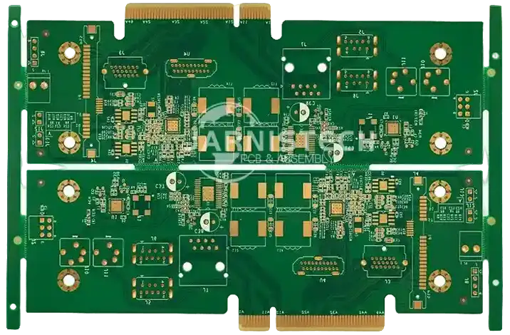
The surface finish of a printed circuit board (PCB) greatly affects its performance in various aspects like solderability, corrosion resistance, and conductivity. A deeper understanding of these technical factors helps reveal how surface finish choices influence the overall quality and dependability of the PCB. From the strength of solder joints to its behavior in high-frequency circuits, the surface finish impacts the lifespan and functionality of the PCB in real-world applications. Selecting the right finish ensures long-lasting reliability and consistent performance throughout the PCB’s service life.
Surface Roughness and Solderability
How Roughness Affects Solder Joint Strength and Reflow Soldering-
Surface roughness is one of the most base factors in determining the solderability of a PCB. It directly influences the adhesion between the solder and the PCB surface, which in turn affects the overall reliability of the solder joints.
●Solder Joint Strength: A smoother surface finish typically leads to better solder joint strength. When the surface finish has a higher roughness, it creates more microscopic gaps where solder can accumulate, improving the mechanical bond. However, excessive roughness can cause uneven solder distribution, leading to weak joints that are prone to failure under thermal cycling or mechanical stress.
●Reflow Soldering Process: Reflow soldering, which is often used for surface mount technology (SMT), requires a surface finish that allows solder to flow evenly across the PCB. A highly polished surface, such as ENIG (Electroless Nickel Immersion Gold), provides a smooth and even surface that helps solder wet evenly across the pads, leading to stronger and more reliable joints. In contrast, rougher finishes may cause uneven solder wetting, leading to cold solder joints that can impact the electrical performance.
●Finishes and Roughness: For finishes like Immersion Tin or Immersion Silver, the roughness is kept relatively low to ensure smooth soldering. While these finishes are not as smooth as ENIG, they are still acceptable for most applications due to their good solderability and uniform coating.
Surface Roughness Impact on Solderability-
| Surface Finish | Surface Roughness | Impact on Solder Joint | Reflow Soldering Effectiveness |
| ENIG | Smooth | High solder joint strength | Excellent wetting, minimal voids |
| Immersion Silver | Low to Medium | Good solder joint strength | Good wetting, minimal cold joints |
| Immersion Tin | Medium | Moderate solder strength | Adequate wetting, some minor issues |
| HASL | High | Moderate to low solder strength | Poor wetting, leads to cold joints |
Corrosion Resistance in Long-Term Applications
Comparing OSP, ENIG, and Immersion Tin Finishes-
Corrosion resistance plays a central part in selecting surface finishes for long-lasting applications, particularly in environments with exposure to moisture, chemicals, or high humidity. For PCBs used in industrial, automotive, or outdoor settings, having resistance to corrosion ensures their durability and continued reliability.
●OSP (Organic Solderability Preservative): OSP is a popular choice for low-cost consumer electronics. It provides a thin organic coating that protects copper from oxidation. While it’s effective at preventing corrosion in the short term, OSP may not be suitable for high-stress or high-humidity environments due to its relatively low durability over time.
●ENIG (Electroless Nickel Immersion Gold): ENIG provides excellent corrosion resistance due to the nickel layer, which acts as a protective barrier against environmental damage. The gold layer on top of the nickel ensures that the surface is not prone to oxidation, making it suitable for long-term and high-reliability applications like aerospace, medical devices, and automotive electronics.
●Immersion Tin: Immersion Tin is also a commonly used finish for PCB applications that require corrosion resistance. While it offers decent protection, it may not be as effective in extreme environments compared to ENIG. However, for standard consumer electronics, immersion tin is an affordable and effective solution for corrosion resistance.
Corrosion Resistance of PCB Surface Finishes-
| Surface Finish | Corrosion Resistance | Best Use Case |
| ENIG | High | Automotive, aerospace, medical |
| Immersion Silver | Moderate | Consumer electronics, RF circuits |
| Immersion Tin | Moderate | Consumer electronics |
| OSP | Low | Low-cost applications |
Thermal and Electrical Conductivity of PCB Surface Finishes
Performance Under High-Power and High-Frequency Conditions-
The thermal and electrical conductivity of a PCB surface finish greatly influences performance in high-power and high-frequency applications. For these applications, the finish must support efficient heat dissipation and reliable electrical signal flow, ensuring the PCB performs properly without overheating or signal loss.
●Electrical Conductivity: ENIG and Immersion Silver offer the best electrical conductivity due to their smooth, uniform surface that minimizes resistance and ensures optimal signal flow. For example, Immersion Silver is often used in RF (radio frequency) applications where signal loss must be minimized.
●Thermal Conductivity: ENIG and Immersion Tin are among the finishes with better thermal conductivity properties. ENIG, with its nickel layer, offers more heat resistance, making it ideal for high-power applications like power supplies and automotive electronics. Immersion Tin, while not as thermally conductive as ENIG, still provides adequate heat dissipation for most consumer electronics.
●High-Power Applications: In high-power applications, such as industrial machinery or power supplies, a robust surface finish that can handle elevated temperatures is necessary. Hard Gold or ENEPIG (Electroless Nickel Electroless Palladium Immersion Gold) finishes are often used for such designs, as they can withstand higher temperatures and maintain signal integrity.
Thermal and Electrical Conductivity of PCB Surface Finishes-
| Surface Finish | Electrical Conductivity | Thermal Conductivity | Best Application |
| ENIG | High | High | High-power, automotive |
| Immersion Silver | Very High | Moderate | RF, high-frequency |
| Immersion Tin | Moderate | Moderate | Consumer electronics |
| Hard Gold | High | Very High | Industrial, power electronics |
| ENEPIG | High | High | Aerospace, automotive |
Common Challenges in PCB Surface Finishing and Solutions
Surface finishing in PCB manufacturing directly impacts the board’s performance and lifespan. However, this process is not free of challenges. Surface finishes can encounter defects that hinder the PCB’s functionality, which may lead to costly delays and rework. Understanding the common problems and how to resolve them is key to producing high-quality boards. Let’s explore some of the most frequent issues with PCB surface finishes and look at the solutions that help tackle them effectively.
Identifying and Preventing Common Defects
PCB surface finishes can suffer from a variety of defects, some of which can be challenging to identify and correct. Among the most common issues are tarnishing, voids, and poor adhesion. Let’s break them down and explore how to tackle these challenges.
Tarnishing-
Tarnishing occurs when the surface finish, particularly finishes like immersion silver or immersion tin, reacts with air or moisture, leading to discoloration and degradation of the finish. This can impact the solderability of the board and cause failures in electrical connections. Tarnishing is a particular concern when handling immersion silver finishes, as silver oxide can form on the surface and interfere with solder joints.
●Solution: To prevent tarnishing, ensure that the boards are stored in a dry, controlled environment, away from exposure to air and moisture. Packaging the PCBs in sealed bags with desiccants can help protect the surface finish during shipping and storage. Additionally, using a gold or palladium finish, such as ENIG or ENIPIG, can minimize tarnishing as these materials are less prone to oxidation.
Voids-
Voids are tiny air pockets that form under the solder joints during reflow soldering. Voids can weaken the electrical connection and cause potential reliability issues, especially in high-density interconnect (HDI) PCBs or when dealing with fine-pitch components.
●Solution: Voids can be reduced by optimizing the soldering process. Ensure that the solder paste is applied evenly and that the reflow profile is carefully controlled. Using immersion tin or immersion silver can help improve the wettability of the solder joints, reducing the chance of void formation.
Poor Adhesion-
Poor adhesion between the PCB surface and the solder mask or component leads can result in delamination, lifted pads, or poor solder joints. This problem is often caused by improper surface preparation, contamination, or issues with the finish itself.
●Solution: Proper surface preparation is the first step in getting a quality PCB surface finish. Before applying any coating, it’s crucial to clean the PCB thoroughly to get rid of any dirt, oils, or other contaminants. This cleaning process ensures that the finish sticks properly and lasts longer. A pre-treatment, like desmearing or plating, can also help by creating a better surface for the finish to bond to. When it comes to surface finishes, options like ENIG (Electroless Nickel Immersion Gold) provide a smoother surface than finishes like HASL, which tend to be more porous. The smoother surface of ENIG helps improve adhesion, making it a solid choice for high-performance applications.
Common Defects in PCB Surface Finishing and Solutions-
| Defect | Description | Solution |
| Tarnishing | Discoloration and degradation of surface finishes | Store in controlled, dry environments, use sealed packaging, or switch to ENIG or ENIPIG |
| Voids | Air pockets under solder joints | Optimize soldering process, use immersion tin or immersion silver |
| Poor Adhesion | Solder mask or component leads lift or peel | Proper surface preparation and pre-treatment, use ENIG for better adhesion |
Optimizing Surface Finish Application Processes
Achieving consistent, high-quality surface finishes on PCBs requires meticulous attention to detail and adherence to best practices throughout the application process. The following best practices can help PCB manufacturers achieve uniform coating, reduce defects, and improve overall finish quality.
Best Practices for Uniform Coating-
●Precision Coating Techniques: To ensure an even coating of surface finish materials, it’s important to use automated systems like selective plating or spraying. These methods control the thickness and uniformity of the coating, preventing issues like uneven plating or excessive buildup in certain areas.
●Process Control: Implementing tight control over the application parameters such as temperature, time, and concentration of plating solutions can significantly reduce defects. For example, in HASL processes, careful temperature control during the solder dipping can prevent over-coating or under-coating, which may result in poor solderability or corrosion.
Material Handling-
●Use of High-Quality Chemicals: The quality of the chemicals used during the surface finishing process can affect both the quality and consistency of the finish. Using high-quality, well-maintained plating solutions will ensure a uniform finish across the entire PCB.
●Cleaning and Preparation: Thorough cleaning of the PCB before applying the surface finish is necessary to remove oils, dirt, and oxidation that can affect the bonding of the finish. Additionally, handling the boards with clean gloves and minimizing exposure to contaminants will help reduce defects in the final finish.
Best Practices for Surface Finish Application-
| Best Practice | Description |
| Precision Coating Techniques | Use automated plating or spraying for even coatings. |
| Process Control | Maintain tight control over temperature, time, and plating solution concentration. |
| Use of High-Quality Chemicals | Ensure the use of high-quality, well-maintained plating chemicals. |
| Cleaning and Preparation | Clean PCBs thoroughly to avoid contamination, and handle with care. |
Storage and Handling of Finished PCBs
Proper storage and handling of finished PCBs ensures the surface finish remains intact and maintains its performance. Improper storage or mishandling can lead to contamination, oxidation, or physical damage, affecting the board’s overall quality. Keeping the PCBs in a clean, controlled environment and taking care during transportation helps to preserve the finish, ensuring the board is ready for optimal performance when needed. With the right precautions, the longevity of the surface finish can be significantly improved.
Tips to Prevent Contamination-
●Sealed Packaging: Finished PCBs should be stored in moisture-resistant bags with desiccants to prevent exposure to humidity. This is especially important for finishes like immersion silver and immersion tin, which are prone to tarnishing and oxidation when exposed to moisture.
●Clean Environment: The storage area should be free of dust, dirt, and any contaminants that could affect the PCB surface. Temperature and humidity control are also crucial to ensure that the PCBs are not exposed to extreme conditions that could degrade the finish.
●Handling with Care: Use clean gloves when handling finished PCBs to avoid leaving oils or residues on the surface. It’s also important to handle the boards by the edges to avoid contaminating or damaging the surface.
Prolonging Shelf Life-
●Shelf Life Considerations: Different finishes have different shelf lives, depending on the material used. Immersion tin and immersion silver finishes have shorter shelf lives and may degrade faster than ENIG or ENIPIG finishes. To extend shelf life, ensure that finished PCBs are stored in optimal conditions and avoid exposing them to extreme temperatures or humidity.
Tips for Storing and Handling Finished PCBs-
| Tip | Description |
| Sealed Packaging | Use moisture-resistant bags with desiccants to prevent oxidation. |
| Clean Environment | Store in a dust-free, temperature and humidity-controlled environment. |
| Handling with Care | Use clean gloves and handle by the edges to prevent contamination. |
| Shelf Life Considerations | Store PCBs in optimal conditions to extend shelf life, especially for finishes like immersion tin and immersion silver. |
Impact of PCB Surface Finish (Surface Method) on Testing and Inspection
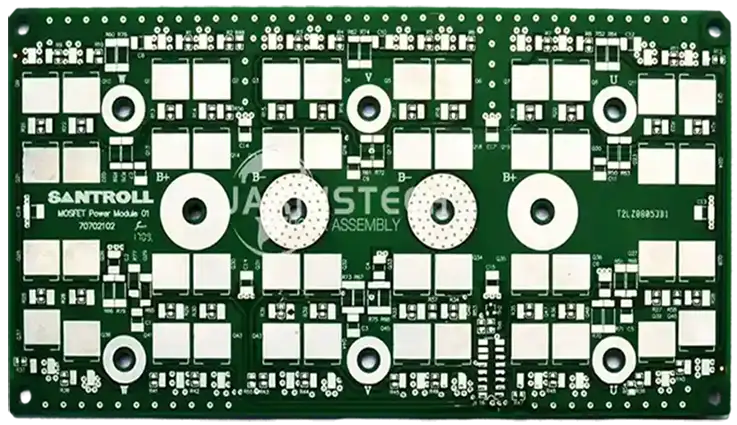
When it comes to testing and inspecting PCBs, the surface finish plays a bigger role than you might expect. Your choice of finish impacts how the board behaves during processes like Automated Optical Inspection (AOI) and In-Circuit Testing (ICT). Different finishes present unique challenges, and you may need to tweak your testing setup to ensure that you get the most accurate results. For example, certain finishes could affect the clarity of the signals detected by the AOI system, or alter the performance of the probes in ICT. Understanding how different finishes interact with your testing equipment is key to getting reliable feedback. Let’s dive into how various surface finishes influence the testing process and what adjustments might be needed for smooth inspection.
Adjusting AOI and ICT for Different Surface Methods
ENIG (Electroless Nickel Immersion Gold) is a commonly used surface finish, but its reflective nature can sometimes make it a headache during testing. The gold layer creates a shiny surface that can interfere with AOI systems, causing glare and making it harder to spot defects.
1.AOI Issues: The shiny finish can mess with the contrast, making it harder for the AOI system to catch small defects, such as misaligned pads. Without adjusting the settings, you might end up with a false pass.
●Solution: Tuning your AOI contrast settings and adjusting the lighting angles can help improve detection. Regular calibration of the AOI system also ensures that it’s able to properly inspect reflective finishes.
2.ICT Issues: When using ICT, the reflective surface can mess with contact impedance and result in inaccurate readings, especially if there’s any gold oxide buildup.
●Solution: Perform a pre-test calibration on the probes and use fixtures that apply more pressure to ensure proper contact, especially on smooth, shiny finishes like ENIG.
Adjustments for AOI and ICT with Reflective Finishes (ENIG)-
| Finish Type | Challenge | Solution |
| ENIG | Shiny surface causes glare in AOI | Adjust contrast and lighting angles, calibrate AOI software. |
| ENIG | Gold plating affects contact impedance in ICT | Perform pre-test calibration, use specialized testing fixtures. |
Ensuring Quality with XRF Analysis and Other Tools
When dealing with surface finishes like ENIG, immersion tin, or immersion silver, it’s necessary to pay attention to factors such as thickness and adhesion. X-ray fluorescence (XRF) analysis is often used to check the consistency of these finishes, particularly regarding thickness. This method provides a reliable way to assess the uniformity of the finish layers, helping ensure that the PCB performs as expected. Monitoring these aspects can help avoid potential issues during the manufacturing process.
1.XRF for Thickness: Using XRF analysis allows you to accurately measure the thickness of the metal layers, ensuring they’re within the required specifications. If the finish is too thin or uneven, it might not offer reliable performance, leading to possible solder joint issues.
●Solution: Regularly check the thickness using XRF tools and take corrective actions if needed. Ensure the finish meets the required standards to avoid performance degradation.
2.Adhesion Testing: Some finishes, like immersion tin, need a strong bond to the copper substrate. Weak adhesion can result in failure, especially during thermal cycling or under stress.
●Solution: Perform adhesion tests like peel tests to verify the strength of the finish and prevent long-term issues.
Advanced Testing Techniques for PCB Surface Finishes-
| Surface Finish | Test Type | Purpose | Tools/Methods |
| ENIG | XRF Analysis | Measure thickness of nickel and gold layers | XRF analyzer |
| Immersion Tin | Adhesion Testing | Ensure adhesion to copper substrate | Peel test, scratch test |
| Immersion Silver | Adhesion Testing | Ensure strong adhesion for reliable performance | Peel test, scratch test |
Common Testing Issues and How to Overcome Them
PCBs don’t always pass the test with flying colors. Surface finishes can lead to issues during functional and environmental testing. Whether it’s poor adhesion, corrosion, or a finish that’s incompatible with the product’s needs, these hurdles can affect performance.
Ensuring Compatibility with Functional and Environmental Testing-
Different surface finishes behave differently in various conditions. For instance, finishes like immersion silver might degrade in high humidity, while HASL can cause problems in high-frequency designs due to its rough surface.
1.Functional Testing Issues: When you’re testing for functionality, an incompatible surface finish can cause issues like poor signal integrity. HASL, for instance, can be uneven, leading to poor electrical contact and potential failures.
●Solution: Choose for finishes like ENIG or immersion silver, which have a smoother surface and are better suited for high-frequency applications. Performing thorough functional testing before mass production ensures that the finish won’t interfere with your design.
2.Environmental Testing Issues: In extreme environments, finishes like immersion tin or HASL can degrade, especially when exposed to humidity, heat, or thermal cycling.
●Solution: Select finishes like ENIG or ENEPIG, which provide better resistance to corrosion and environmental stress. Environmental tests, such as thermal cycling and humidity exposure, should be used to confirm that the finish can handle the intended conditions.
Addressing Common Testing Issues-
| Testing Area | Challenge | Solution |
| Functional Testing | Poor finish causes signal loss or functional failure | Use finishes like ENIG or immersion silver, conduct functional validation tests. |
| Environmental Testing | Surface finishes degrade under harsh conditions | Use ENIG, ENEPIG for better corrosion and oxidation resistance. Conduct environmental tests like thermal cycling. |
Innovations and Hybrid Solutions in PCB Surface Finish Methods
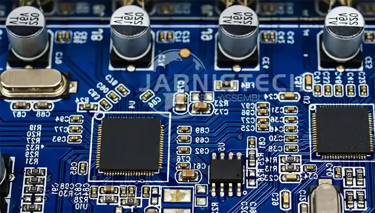
In the constantly evolving world of electronics manufacturing, the need for more durable, reliable, and cost-effective PCB surface finishes has pushed the boundaries of traditional methods. Hybrid solutions and emerging technologies are reshaping the landscape, with innovative surface finishes offering distinct advantages for specialized industries like automotive, aerospace, and medical devices. This section explores these advancements, including hybrid finishes like ENIPIG (Electroless Nickel Immersion Palladium Immersion Gold) and emerging technologies that promise to enhance the PCB manufacturing process.
Emerging Hybrid Finishes: ENIPIG and Beyond
ENIPIG, a hybrid surface finish that combines Electroless Nickel, Immersion Palladium, and Immersion Gold, has emerged as a strong alternative to traditional ENIG finishes. This hybrid finish offers a number of advantages that make it an appealing choice for high-reliability applications, particularly in industries that demand exceptional performance under extreme conditions.
●Improved Solderability: Palladium, the unique element in ENIPIG, enhances the solderability of the PCB surface. It provides a more uniform, smoother finish compared to gold alone. This is especially beneficial for fine-pitch components and smaller, more complex designs, where even the slightest soldering issue could lead to failure.
●Superior Corrosion Resistance: Palladium provides better resistance to oxidation compared to gold, making it a preferred option in environments where exposure to moisture and chemicals is common. This feature helps ensure the long-term reliability of PCBs in challenging conditions. ENIPIG is often selected for demanding applications like automotive, aerospace, and high-frequency communication. These fields require finishes that can handle the rigors of harsh conditions while maintaining dependable performance.
●Cost-Efficiency: While ENIPIG can be more expensive than ENIG due to the use of palladium, the additional advantages it offers in terms of longevity and performance justify the cost for high-end applications. The overall cost can be further optimized by combining ENIPIG with other finishes in a selective finishing process, balancing performance and budget.
Comparison Between ENIPIG and ENIG-
| Surface Finish | Key Features | Best Applications |
| ENIPIG | Palladium enhances solderability, superior corrosion resistance | Automotive, aerospace, high-frequency applications |
| ENIG | Smooth finish with excellent solderability | Consumer electronics, general-purpose applications |
Future Technologies in Surface Finishing
As the electronics industry advances, Artificial Intelligence (AI) and automation are beginning to play a transformative role in PCB surface finishing. AI-assisted inspection systems are already improving the accuracy and speed of the inspection process, helping manufacturers detect defects in the surface finish more efficiently and accurately.
●AI-Assisted Inspection: AI technologies, such as machine learning and computer vision, allow for faster detection of inconsistencies and defects in the surface finishes. These systems can quickly analyze large volumes of PCB data to identify imperfections that would typically be missed during manual inspection, improving both quality control and yield rates. This technology ensures that only the highest-quality boards make it to the next stages of assembly.
●Automated Application Processes: The application of surface finishes is becoming increasingly automated, reducing the likelihood of human error and improving consistency across production batches. Automated dispensing systems can precisely apply the right finish to specific areas of the PCB, particularly in selective finishing processes. This level of precision is necessary for ensuring the integrity of sensitive components, such as those used in medical or high-frequency applications.
●The Future: Looking ahead, robotic systems may completely revolutionize how surface finishes are applied. These systems could work with an unparalleled level of precision, applying multiple finishes to a single PCB based on its design and requirements. Such innovations will streamline the PCB production process, reduce costs, and increase throughput while maintaining high quality.
Future Technologies in PCB Surface Finishing-
| Technology | Description | Impact on PCB Manufacturing |
| AI-Assisted Inspection | Machine learning and computer vision used for defect detection | Faster and more accurate inspections, reduced error rates |
| Automated Application | Precise application of finishes using robotic systems | Increased consistency, reduced labor costs, higher throughput |
| Robotic Systems | Advanced robotic systems for surface finish application | Revolutionizes production processes, increased precision and speed |
FAQ & PCB Surface Finish
Can PCB surface finishes be mixed on the same board?
Yes, different finishes can be applied to different areas of the same PCB depending on the requirements, such as using ENIG for signal areas and HASL for non-critical areas.
What is the lifespan of a PCB surface finish?
The lifespan of a PCB surface finish varies by type. ENIG generally offers a longer lifespan compared to finishes like immersion tin, which can degrade quicker due to environmental factors.
How does surface finish affect environmental performance?
Some finishes, like immersion tin and HASL, may degrade under extreme environmental conditions (like high humidity or thermal stress), while ENIG and ENEPIG offer better corrosion resistance and durability.
Contact Jarnistech for More Information on PCB Surface Finishes
With so many options to pick from, it’s difficult to decide the best one for your specific application. Luckily, JarnisTech will assist you through the entire process.
JarnisTech is a manufacturer of printed circuit boards offering small-batch and large-volume PCBs to people all over the world. As an ISO-9001 certified PCB manufacturer, We have years of experience with printed circuit boards as well as their intricate details. Since PCBs and PCB components are what we specialize in and we are able to answer any you might have about this type of technology.
If you’d like to know more about PCB’s surface finish and to explore the possibilities, contact us today by completing our form or by calling us at 0086-755-23034656

