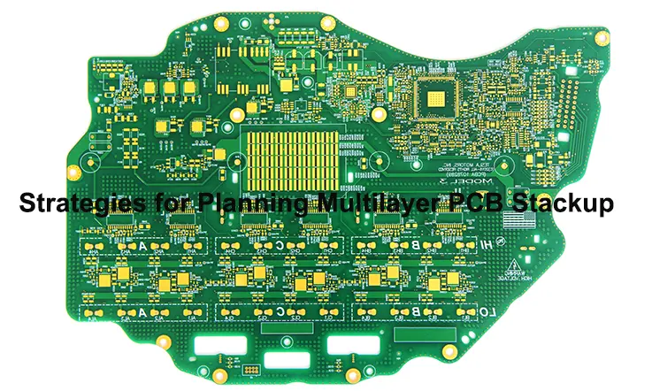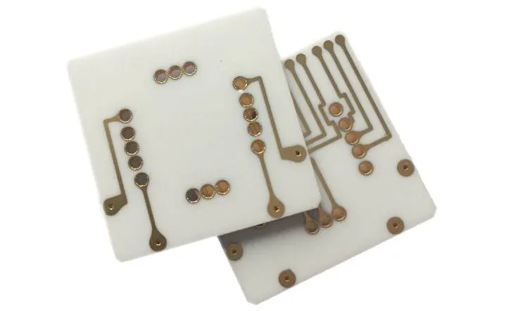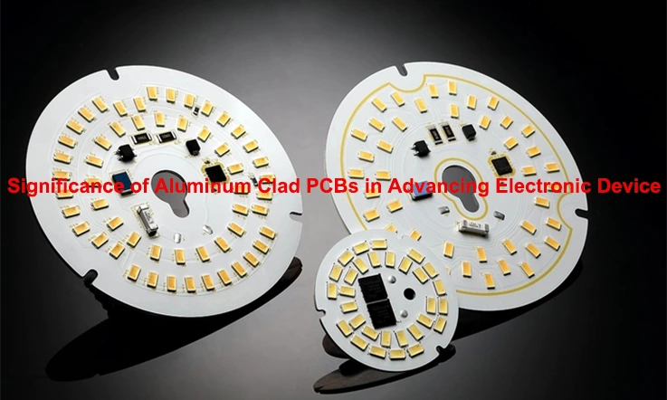
When it comes to designing and producing printed circuit boards (PCBs), there’s no room for error. Whether you’re designing PCBs for consumer electronics, medical devices, or automotive systems, the goal is always the same: ensure reliability, precision, and efficiency. Yet, one of the most overlooked aspects of PCB design and production is the quality assurance (QA) process that ensures a flawless product.
PCB Quality Assurance is the foundation of consistent, reliable production. It ensures that your board not only works but performs optimally in its intended environment. As electronic products become more complex and PCB layouts push the boundaries of miniaturization, QA has evolved far beyond simple defect detection.
With smaller designs and tighter tolerances, there’s more at stake. Quality assurance today is about much more than checking for faults—it’s about making sure every detail is dialed in, so the end product holds up under real-world conditions.
In this article, we’ll break down effective QA techniques, modern inspection methods, and the future of PCB quality control. This isn’t just about inspecting a few components; it’s about implementing a holistic strategy that spans the entire lifecycle of the PCB—from design to testing, fabrication, and assembly. We’ll also touch on industry standards, best practices, and the latest advancements that help PCB manufacturers deliver top-notch, reliable PCBs.
PCB Quality Assurance and its Importance in the PCB Manufacturing Process
PCB quality assurance is a broad term that encompasses a range of inspection and testing procedures designed to ensure that every PCB meets required standards. But let’s break it down—what does this mean, practically speaking?
●The process begins with validating the design. Before any PCB moves into production, it’s important to confirm that the design follows best practices in Design for Manufacturability (DFM). This includes verifying that the design is suitable for efficient fabrication, assembly, and testing. If the design isn’t validated properly, it can lead to problems that snowball throughout the manufacturing stages, making it harder to address quality control issues later on.
●Once manufacturing begins, quality assurance continues with multiple layers of inspection. Automated Optical Inspection (AOI), X-ray inspection, and functional testing all serve to catch defects early before the PCB reaches the final customer. But it’s not just about preventing defects—QA is also about optimizing performance and ensuring that the end product will work as intended in its final application, whether that’s in consumer electronics, medical devices, or automotive systems.
●Each PCB assembly undergoes stringent testing protocols to check for component integrity, electrical continuity, and solder joint quality. This ensures that every component, whether it’s a small capacitor or a complex microprocessor, is securely placed and functioning properly.
The Relationship Between PCB Quality and End-Product Performance
●To understand the full impact of PCB quality assurance, consider the connection between the PCB itself and the final product’s performance. A PCB is more than just a simple circuit board—it’s the lifeblood of the device it supports. When designed and manufactured properly, a PCB ensures that the device operates at peak efficiency, delivering the performance that users expect.
For instance, take the example of medical devices. These products require the highest level of precision, as even the smallest PCB defect can lead to malfunctioning equipment. PCBs in medical devices often carry sensitive signal traces that monitor vital patient data. A defect could result in incorrect readings, causing potentially life-threatening mistakes.
●Similarly, in consumer electronics, where PCBs handle everything from power regulation to signal transmission, the quality of the PCB directly affects the device’s reliability and longevity. If a PCB is made with low-quality components or lacks proper testing, you might see performance degradation over time, such as screen flickering, audio distortion, or even device shutdowns.
A good example is in the realm of smartphones. With an average lifespan of only 2–3 years, if the PCB in your smartphone isn’t built to withstand stress over time, you’ll quickly run into issues with battery performance, signal reception, and overall device durability. However, when the PCB quality assurance process is followed closely, it ensures that each component functions properly and the board can endure continuous use, providing customers with a long-lasting device.
Here’s a the key relationship between PCB quality assurance and end-product performance across various industries:
| Industry | PCB Application | Impact of Quality Assurance |
| Consumer Electronics | Smartphones, Laptops, Tablets | Affects power efficiency, signal integrity, and durability |
| Medical Devices | Pacemakers, Diagnostic Equipment | Ensures precise signal transmission and safety |
| Automotive Systems | Infotainment, GPS, Sensors | Impacts safety features, performance, and longevity |
| Industrial Equipment | Machinery Controllers, Robotics | Affects system reliability, safety, and operational uptime |
How PCB Quality Assurance Ensures High Reliability and Cost-Efficiency in Production?
At first glance, you might think of quality assurance as just an added step—something that increases costs and time. But in reality, it’s a money-saving strategy that prevents the much higher costs associated with defective products, warranty claims, and recalls. Quality assurance helps to streamline the manufacturing process by catching issues early, avoiding production bottlenecks, and ensuring that only the highest-quality PCBs are delivered to customers.
Moreover, investing in preventive maintenance and design validation can eliminate the need for expensive redesigns and rework. By ensuring that PCBs are designed with manufacturability in mind, we can avoid issues such as misaligned components or improper soldering that would require redoing an entire batch. This helps reduce waste and make the entire production process more cost-effective.
Key Elements of PCB Quality Assurance in Manufacturing
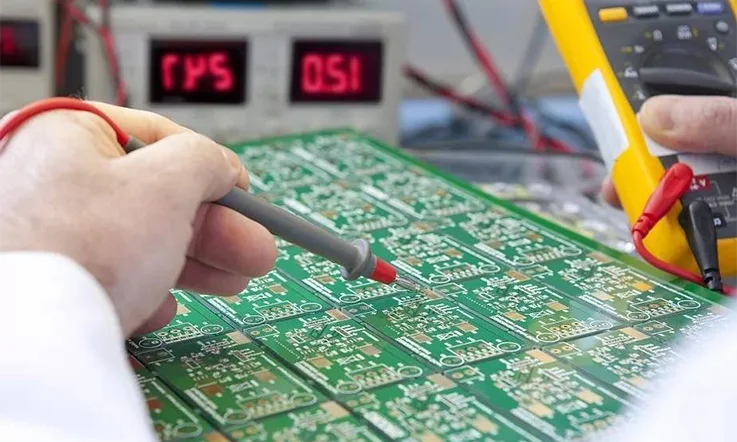
Achieving top-tier PCB quality assurance doesn’t just happen by chance—it involves a thorough process that spans design, fabrication, and assembly. A well-structured PCB manufacturing process includes rigorous checks and quality control at every stage, from design for manufacturability (DFM) to automated optical inspection (AOI). By focusing on these key elements, we can ensure that our PCBs meet the necessary standards for reliability and performance, reducing the risk of failure and increasing customer satisfaction.
PCB Design for Manufacturability (DFM) and Its Impact on PCB Quality Assurance
When it comes to achieving consistent PCB quality, Design for Manufacturability (DFM) is one of the first checkpoints. DFM is a process that ensures the PCB design is optimized for efficient and cost-effective manufacturing, reducing the likelihood of design errors that can lead to defects. When DFM guidelines are incorporated into the design phase, the design team works to create PCBs that are easy to assemble and that comply with industry standards such as IPC-A-600.
How DFM Benefits PCB Quality Assurance-
1.Reduced Design Errors: DFM helps identify potential design flaws early in the process, such as trace width issues, unoptimized component placement, or insufficient clearance between components. By catching these issues before production, we can help our clients save both time and money.
2.Improved Manufacturability: By designing PCBs with manufacturability in mind, our designers can ensure that the boards are easy to produce and assemble, reducing production delays and lowering the chances of defects.
3.Compliance with Industry Standards: DFM helps ensure that PCBs meet industry standards like IPC-A-600 (the standard for PCB quality assurance). These standards define acceptable quality levels for soldering, trace widths, and component placement, ensuring the PCB will function correctly in its final application.
1.Best Practices for Incorporating DFM into the Design Process:
●Early Collaboration: Involve PCB manufacturing engineers and quality control experts early in the design phase to ensure DFM principles are followed.
●Use DFM Software Tools: Use advanced software tools to simulate the manufacturing process and identify potential issues before physical production begins.
●Optimize Component Placement: Ensure components are placed efficiently to minimize the chances of misalignment or other assembly issues.
Understanding PCB Fabrication Standards for Consistent Quality
Fabrication standards form the foundation of any effective PCB manufacturing process. These standards guarantee that each PCB is produced according to the exact specifications, ensuring uniform quality across the board. Key areas of focus include managing tolerances, maintaining proper layer alignment, and controlling trace widths. Each of these factors directly impacts the overall functionality and performance of the PCB, ensuring it meets reliability requirements and performs well in its intended environment.
Defining Fabrication Standards for Consistent PCB Quality Assurance-
1.Tolerance Control: Tight tolerance management ensures that the PCB is within the correct dimensions, preventing issues like misalignment and ensuring the PCB fits correctly in its intended enclosure.
2.Layer Alignment: For multi-layer PCBs, ensuring precise layer alignment throughout the fabrication process is a must. Any misalignment can lead to serious issues like signal loss or electrical faults, which can compromise the performance and reliability of the final product. Maintaining tight tolerances and careful alignment during each step of the process minimizes these risks, resulting in a board that functions as intended without unwanted surprises.
3.Trace Width and Spacing: Ensuring that trace widths and spacings are within acceptable limits is necessary for the board’s performance. Too wide or too narrow traces can cause signal integrity issues or increase the risk of shorts.
1.Why Tight Tolerance Management Matters for PCB Quality:
●Consistency in Performance: Properly aligned layers and controlled trace widths ensure the PCB operates consistently, preventing issues like crosstalk or signal loss.
●Reduced Scrap Rates: With tight tolerance management, there is less waste due to defective boards, which translates into cost savings and more reliable PCBs.
2.Best Practices for PCB Fabrication:
●Use High-Precision Tools: Invest in advanced equipment that guarantees accurate trace widths, tight layer alignment, and superior tolerance management.
●Continuous Monitoring: Implement real-time monitoring during the fabrication process to catch any issues early and adjust before the board moves to the next stage.
Automated Optical Inspection (AOI) for PCB Defect Detection
One of the most effective methods for detecting defects in PCBs is Automated Optical Inspection (AOI). AOI is a powerful tool used during the PCB assembly phase to identify issues such as soldering defects, misalignments, and etching problems. With the help of 3D AOI systems, manufacturers can now detect even the smallest imperfections that might otherwise go unnoticed.
How AOI Enhances PCB Quality Assurance-
1.Detecting Soldering Defects: AOI uses high-resolution cameras to inspect solder joints for defects like cold solder joints or bridging, both of which can cause the PCB to malfunction.
2.Misalignment Detection: AOI systems can also identify issues with component placement, such as misaligned chips or incorrectly placed resistors, ensuring that the PCB meets the specified design.
3.Etching Problems: AOI systems also help detect issues with etching, such as uneven copper traces or missing traces, which can compromise the PCB’s functionality.
The Role of 3D AOI in Improving Yield Rates:
●Real-Time Feedback: AOI systems provide real-time feedback, enabling manufacturers to catch defects early in the assembly process and make quick corrections. This helps reduce the number of faulty boards in the final product.
●Higher Yield Rates: With 3D AOI, manufacturers can inspect PCBs from all angles, ensuring a more thorough inspection and higher yield rates for the production line.
Best Practices for AOI in PCB Manufacturing:
●Integrate AOI Early in the Assembly Process: Start AOI inspections early to catch defects at the earliest possible stage.
●Customize AOI Settings: Tailor the AOI system’s settings to the specific PCB design to ensure more accurate defect detection.
●Combine AOI with Other Inspection Techniques: While AOI is powerful, combining it with X-ray inspection and functional testing can provide a more comprehensive approach to PCB quality assurance.
Advanced Testing and Inspection Methods for PCB Quality Assurance
When it comes to ensuring that PCBs meet the highest standards of quality assurance, advanced testing and inspection methods play an indispensable role. With the growing complexity of modern PCB designs, electrical testing, X-ray inspection, and visual and functional testing are critical components of a robust quality control process. These tests are the detectives of the process—they dig deep to uncover hidden issues, double-check the design, and confirm that the PCB performs like it’s supposed to, even when it’s put to the test in real-world environments.
Electrical Testing: Validating PCB Functionality and Performance
Electrical testing is a fundamental part of PCB quality assurance, ensuring that the PCB functions as expected and aligns with the design requirements. This process involves assessing electrical aspects such as signal integrity, power distribution, and component performance. By carefully evaluating these factors, We can confirm that the PCB will operate reliably when integrated into the final product, minimizing the risk of issues down the line.
In-circuit testing (ICT) is one of the most effective methods for checking the integrity of the PCB and its components. This involves placing test probes on the PCB’s nodes and measuring voltages, currents, and resistances to ensure each component is connected properly and functions within the specified range. With boundary scan testing, additional diagnostic capabilities are provided, allowing for testing without physical contact with the components, especially in cases where the components are hidden beneath the surface.
Automated Testing Systems (ATS), which are commonly used in high-volume PCB production, allow for quick and consistent testing of each board. These systems can automatically detect short circuits, open circuits, and component misplacements, and flag any issues for correction before proceeding to the next stage of production.
1.Best Practices for Electrical Testing-
●Pre-test Validation: Ensure that all PCB designs are verified before electrical testing to catch design issues early.
●Multi-stage Testing: Use a combination of ICT, boundary scan, and ATS to test different stages of the manufacturing process, improving fault detection accuracy.
●Temperature Compensation: Account for temperature variations that can affect circuit behavior during testing.
By adopting these best practices, we can ensure that their PCBs meet the desired performance standards and will operate reliably in the end-product.
X-Ray Inspection: Ensuring Hidden Defect Detection in Multi-Layer PCBs
In today’s world of multi-layer PCBs, traditional inspection methods often fall short when it comes to detecting defects hidden within the layers of the board. That’s where X-ray inspection comes in. X-ray inspection is a non-destructive method used to check internal components and connections, making it especially useful for high-density interconnect (HDI) boards and stacked vias.
One of the most significant advantages of X-ray inspection is its ability to reveal hidden solder joint issues that are not visible with optical inspection. It allows inspectors to view the internal structure of the PCB, such as vias, solder balls, and pad-to-pad connections, ensuring that they are correctly formed and free from defects like cold solder joints or voids. This type of inspection is especially beneficial when dealing with complex designs that feature multiple layers of copper traces, components, and vias.
1.How X-Ray Inspection Works-
●Internal Imaging: X-ray passes through the PCB, capturing detailed images of internal layers and hidden connections.
●Defect Detection: Software analyzes the images for any inconsistencies such as poor solder joints or unfilled vias.
●Real-time Feedback: Inspection results can be immediately provided, allowing manufacturers to address issues before they escalate.
A comparison with other inspection techniques shows how X-ray stands out in cases where other methods, like AOI (Automated Optical Inspection) or visual inspection, might miss defects in internal components.
| Inspection Method | Strengths | Limitations |
| X-Ray Inspection | Detects internal defects in multi-layer boards | Expensive setup, requires specialized equipment |
| AOI (Automated Optical Inspection) | Ideal for detecting surface defects like misalignment and soldering issues | Cannot inspect internal layers or hidden connections |
| Visual Inspection | Quick and simple for surface-level checks | Limited to visible defects, misses hidden issues |
X-ray inspection ensures that even the smallest internal defects are caught early, improving the overall reliability of the PCB and ensuring that the final product meets design specifications.
Visual and Functional Testing for Quality Assurance in PCB Manufacturing
While electrical testing and X-ray inspection are effective methods for spotting hidden defects within a PCB, visual inspection and functional testing ensure the board’s performance in practical scenarios. Visual inspection checks the alignment and soldering quality of components, ensuring that all parts are correctly placed and securely attached. Functional testing goes a step further by simulating real-world conditions to confirm that the PCB operates as expected in its intended environment.
Visual inspection is often one of the first steps in the quality control process. Experienced inspectors utilize high-powered magnification tools or automated optical inspection systems (AOI) to thoroughly check each PCB for potential defects. This includes scrutinizing solder joints, ensuring proper component placement, and verifying trace continuity. Even small imperfections—like a slightly off-center component or a cold solder joint—can throw a wrench in the works, causing performance issues or even complete system failure down the line. A well-executed visual inspection ensures that these issues don’t go unnoticed and that the PCB will hold up under the stresses of its application.
Functional testing, on the other hand, simulates how the PCB will behave in its final application. This could involve powering up the PCB and testing how well it communicates with other systems, how it handles thermal stress, and how it functions under load. For example, oscilloscopes are often used to test the timing of signals, while thermal imaging can identify overheating components that may indicate a design flaw.
1.Best Practices for Visual and Functional Testing-
●Thorough Pre-Assembly Visual Inspection: Ensure all components are correctly placed and oriented before moving forward with functional testing.
●Real-world Simulation: Test the PCB under conditions that closely mimic real-world usage to ensure that the device will perform reliably.
●Comprehensive Functional Checks: Utilize tools like oscilloscopes and thermal cameras to measure electrical signal integrity and detect potential heat-related issues.
Functional testing, coupled with visual inspection, ensures that the PCB won’t just meet design specifications but also perform reliably in its intended environment.
Process Control Techniques for Ensuring PCB Quality Assurance
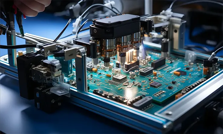
Effective process control methods are at the core of ensuring top-notch quality in PCB manufacturing. By continuously monitoring and tweaking production processes, PCB manufacturers can make sure each board hits the mark in terms of performance and reliability. Process control doesn’t just help spot defects—it’s also a tool for driving continuous improvements that trim costs and boost overall efficiency.
In this section, we’ll break down Statistical Process Control (SPC) techniques, Lean Manufacturing practices, and strategies for ongoing improvement, all of which are elements of modern PCB production quality management.
Implementing Statistical Process Control (SPC) for Quality Management
Statistical Process Control (SPC) is a cornerstone in PCB quality assurance, providing manufacturers with the tools needed to monitor and control production processes to ensure consistency and minimize defects. SPC uses statistical methods to analyze production data and detect any deviations from expected performance. By keeping processes within tolerances, manufacturers can prevent defects before they occur, leading to higher yield rates and better cost efficiency.
How SPC Improves PCB Quality Assurance-
| SPC Tool | Description | Impact on PCB Manufacturing |
| Control Charts | Graphical representations of data points over time | Helps identify trends, shifts, or abnormalities in production |
| Process Capability Indices (Cp, Cpk) | Measures how well a process produces outputs within specified limits | Ensures that manufacturing processes meet customer requirements |
| Six Sigma Techniques | A methodology aimed at reducing defects to less than 3.4 per million opportunities | Improves overall process performance and consistency |
SPC allows PCB manufacturers to catch issues early, adjust production parameters, and continuously improve processes to meet the ever-increasing demand for quality and efficiency.
Lean Manufacturing and Its Effect on PCB Quality Assurance
Lean manufacturing is a philosophy focused on minimizing waste while maximizing value for the customer. When applied to PCB manufacturing, it significantly impacts quality assurance by streamlining operations, reducing unnecessary steps, and improving workflow efficiency. By embracing Lean principles, PCB manufacturers can better focus on value-added activities and reduce production inefficiencies that lead to defects and poor-quality boards.
How Lean Manufacturing Enhances PCB Quality-
| Lean Principle | Application in PCB Manufacturing | Impact on PCB Quality Assurance |
| Kaizen (Continuous Improvement) | Regular small improvements in the PCB production process | Leads to incremental improvements in production efficiency and defect reduction |
| Value Stream Mapping | Visualizing the entire production process to identify and eliminate waste | Optimizes the flow of materials and reduces unnecessary steps that lead to defects |
| Root Cause Analysis | Identifying the source of defects to implement corrective actions | Prevents recurring issues and enhances long-term PCB quality |
Lean manufacturing not only reduces waste but also improves the responsiveness of the manufacturing process, allowing teams to quickly adjust and maintain high-quality standards. By focusing on eliminating non-value-added activities, PCB manufacturers can reduce defects and improve overall product reliability.
Enhancing Process Control through Continuous Improvement
Continuous improvement is at the heart of a solid quality management system. In PCB manufacturing, this approach keeps processes on their toes, helping us adapt to new challenges and exceed expectations over time. With tools like feedback loops, collaborative problem-solving teams, and thorough quality audits, the goal is to ensure that PCB production quality keeps getting better, rather than plateauing. These practices help make sure that the product stays up to snuff and consistently meets higher standards as time goes on.
Key Continuous Improvement Techniques for PCB Manufacturing-
| Continuous Improvement Method | Description | Impact on PCB Quality Assurance |
| Feedback Loops | Gathering input from production staff and customers to make adjustments | Promotes a culture of improvement and helps address issues promptly |
| Problem-Solving Teams | Cross-functional teams that focus on identifying and solving production problems | Ensures the team works together to address root causes and implement solutions |
| Quality Audits | Regular assessments of the PCB quality management system to ensure compliance with standards | Provides data-driven insights into process performance and areas for improvement |
By focusing on continuous improvement, we can ensure that our PCB production processes adapt to evolving customer needs and industry standards. Through consistent evaluation and adjustment, we can keep our production lines running at peak efficiency and minimize defects over time.
International Standards and Certifications for PCB Quality Assurance
In the PCB manufacturing industry, adhering to international standards and certifications is an effective strategy for ensuring consistent product quality and building customer trust. Certification not only validates a PCB manufacturer’s commitment to quality but also provides a structured approach to achieving and maintaining high standards across production processes. In this section, we will explore the significance of certifications such as IPC-A-600, ISO 9001, RoHS, and UL, and how compliance with these standards can enhance your PCB quality assurance program.
Compliance with IPC-A-600 and Other Industry Standards
IPC-A-600, a standard from the Institute of Printed Circuits (IPC), is the leading guideline for evaluating the quality of printed circuit boards. This industry standard focuses on ensuring that the PCB meets design specifications and performs reliably throughout its lifecycle. Adhering to IPC-A-600 helps PCB manufacturers prevent common defects, manage assembly issues, and achieve higher levels of performance.
Key Elements of IPC-A-600 Compliance-
| Standard | Scope | Key Impact on PCB Quality Assurance |
| IPC-A-600 | Sets the criteria for PCB acceptability, covering aspects such as soldering, vias, and trace quality | Ensures PCBs are manufactured to meet design specifications, reducing defects like open circuits and shorts |
| IPC-2221 | Addresses design and fabrication guidelines for PCB manufacturing | Defines crucial fabrication tolerances and design rules for ensuring the PCB’s manufacturability and reliability |
| IPC-6012 | Relates to the performance and qualification of rigid PCBs | Ensures that rigid boards meet performance standards, improving durability and operational reliability |
Maintaining Compliance with industry standards such as IPC-A-600 is an ongoing process. Regular audits, employee training, and updates to equipment and processes are necessary to stay aligned with evolving standards. we that stay on top of these standards can boost our credibility and meet customer expectations, leading to more successful, long-term partnerships.
Achieving ISO 9001 Certification for PCB Manufacturers
ISO 9001 is a globally recognized standard for quality management systems (QMS) that applies to various industries, including PCB manufacturing. The certification demonstrates a commitment to consistent quality in production and operational efficiency. For PCB manufacturers, ISO 9001 serves as a benchmark for implementing robust management practices and ensuring that PCB products consistently meet customer expectations.
How ISO 9001 Drives PCB Quality Assurance-
| ISO Standard | Focus Area | Impact on PCB Quality Assurance |
| ISO 9001 | Focuses on process optimization, risk management, and customer satisfaction | Provides a framework for improving manufacturing processes, reducing errors, and increasing customer trust |
| ISO 14001 | Environmental management and sustainability | Ensures eco-friendly practices, helping meet environmental regulations and reduce waste |
| ISO/TS 16949 | Quality management for the automotive industry | Addresses the specific needs of automotive PCBs, ensuring higher standards for manufacturing processes |
Achieving ISO 9001 certification involves more than just completing a checklist. It requires consistent monitoring of process performance, adherence to standard operating procedures (SOPs), and the implementation of continuous improvement processes. Regular internal audits and the ability to document and respond to non-conformances are essential for maintaining this certification.
Other Certifications Impacting PCB Quality Assurance
Beyond ISO 9001, there are other certifications that can have a significant impact on PCB quality, especially as they pertain to safety, environmental responsibility, and product reliability.
RoHS (Restriction of Hazardous Substances) is a directive from the European Union aimed at limiting the use of certain hazardous materials in electrical and electronic products. For PCB manufacturers, RoHS compliance ensures that the PCBs do not contain materials like lead, mercury, and cadmium, which are harmful to both the environment and human health.
UL Certification, from Underwriters Laboratories, is another important certification for PCBs. UL certifies that PCBs meet safety standards for fire resistance and electrical performance, ensuring the PCB’s safety in a wide range of applications, from consumer electronics to medical devices and automotive products.
Impact of Key Certifications on PCB Quality Assurance-
| Certification | Scope | Impact on PCB Quality Assurance |
| RoHS | Limits hazardous substances in PCB materials | Ensures environmentally compliant production, reducing exposure to harmful substances |
| UL | Focuses on safety and fire resistance of PCBs | Confirms that PCBs meet safety standards, especially for fire resistance and electrical stability |
| ISO 9001 | Quality management system for continuous improvement | Establishes a foundation for consistent quality, performance, and customer satisfaction |
| IPC-A-600 | Defines acceptable standards for PCB appearance and integrity | Ensures PCBs meet performance expectations and minimize defect rates |
Why Certifications Matter for PCB Manufacturers?
Certifications are not just about meeting a set of requirements; they are a strategic way to ensure PCBs meet high standards and are market-ready. When manufacturers achieve certifications such as RoHS, UL, or ISO 9001, they demonstrate that they are committed to quality and sustainability. These certifications also increase customer confidence, as clients are more likely to trust a manufacturer with established quality credentials.
Maintaining Certification-
While obtaining these certifications is an achievement, maintaining them requires ongoing effort. Regular audits, performance reviews, and internal assessments are necessary to ensure that PCB manufacturers continue to meet these standards. Additionally, It’s not just about meeting them once—it’s about staying ahead by adapting to changes in regulations and industry practices. Staying in the loop with updates ensures you’re not left behind and helps maintain a competitive edge.
Identifying and Resolving Common PCB Defects for Better Quality Assurance
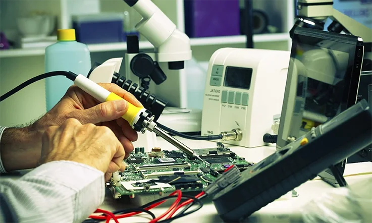
In PCB manufacturing, defects are an inevitable part of the process. Whether dealing with simple single-layer boards or more complex multi-layer designs, issues like open circuits, short circuits, and signal integrity problems can surface at various stages. Tackling these defects swiftly is the step to boosting PCB quality and ensuring the final product meets the required performance and reliability standards. By addressing these issues early in the process, we can prevent costly errors and improve overall production efficiency.
In this section, we’ll dive into several key techniques for identifying and solving common PCB defects. From troubleshooting basic issues like open circuits and short circuits to managing more complex challenges in high-speed designs, you’ll find practical insights to improve your manufacturing processes.
Troubleshooting and Preventing Open Circuits and Shorts
Open circuits and short circuits are two of the most common electrical faults that can undermine the functionality of a PCB. These problems are often rooted in issues like poor soldering, incorrect component placement, and manufacturing defects. The challenge lies in detecting and fixing them without impacting the overall PCB production timeline.
1.Open Circuits-
An open circuit occurs when there is an unintended break in the electrical path, preventing current from flowing through the desired path. This can happen due to issues like poor soldering, component misplacement, or trace damage.
Preventive Measures:
●In-Circuit Testing (ICT): This testing method verifies the continuity of the electrical path and can quickly identify open circuits.
●Automated Optical Inspection (AOI): AOI systems help detect visible open circuits by examining solder joints and PCB traces.
●X-Ray Inspection: X-ray imaging can be useful in inspecting internal layers of multi-layer PCBs, especially to detect hidden open circuits.
| Defect | Causes | Testing Methods | Solution |
| Open Circuit | Poor soldering, misaligned components | In-circuit testing, AOI, X-ray inspection | Rework soldering, inspect trace continuity |
| Short Circuit | Excess solder, contaminated PCB | Visual inspection, electrical testing, AOI | Clean the PCB, rework solder joints |
2.Short Circuits-
Short circuits occur when unintended electrical connections form between two paths, allowing current to bypass components and potentially causing malfunctions. These faults can result from excess solder, poor cleaning, or misplaced components.
Preventive Measures:
●Visual Inspection: A manual or automated visual inspection is the first line of defense against solder bridges that could create short circuits.
●Electrical Testing: Using tools like continuity testers and automated test equipment (ATE) helps detect electrical shorts during or after assembly.
3.Best Practices for Preventing Defects-
●Ensure solder paste application is precise to prevent excessive solder that can lead to bridging.
●Optimize reflow oven profiles to achieve proper solder joint formation and minimize the risk of cold joints or solder bridges.
●Conduct regular automated visual inspections throughout the assembly process to catch defects before they impact the final product.
Managing Signal Integrity and High-Speed PCB Defects
As PCBs evolve to handle high-speed applications, maintaining signal integrity becomes increasingly complex. Issues like trace impedance mismatches, crosstalk, and reflection can seriously degrade the performance of high-speed designs, causing data loss or communication failures.
Signal Integrity Issues in High-Speed Designs-
●Trace Impedance: Improperly routed traces can lead to impedance mismatches, causing signal degradation and reflection.
●Crosstalk: Close traces that carry high-frequency signals can cause interference with one another, distorting the signals.
●Signal Reflection: This occurs when there’s a mismatch in the impedance between the transmission line and its termination point, leading to signal loss or echo.
| Signal Integrity Issue | Cause | Solution |
| Impedance Mismatch | Trace width or spacing inconsistencies | Use controlled impedance routing techniques |
| Crosstalk | Traces placed too close to one another | Implement proper trace spacing, use ground planes |
| Signal Reflection | Inconsistent termination or long traces | Use termination resistors and minimize trace lengths |
Techniques for Preventing Signal Integrity Issues-
1.Controlling Trace Impedance: Ensure that trace widths and spacing follow impedance-controlled routing guidelines to prevent signal reflections and losses. This can be verified using a TDR (Time Domain Reflectometer).
2.Crosstalk Mitigation: Maintain a sufficient distance between signal traces, and use ground planes to isolate sensitive paths from each other.
3.Termination Techniques: Properly terminate long traces using resistors to prevent reflections that could distort high-speed signals.
Advanced Tools for Signal Integrity Testing:
●Signal analyzers and oscilloscopes are essential for analyzing high-speed signals and assessing the quality of waveforms. These tools help evaluate the integrity of electrical signals, ensuring precise performance and identifying any potential issues.
●Network Analyzers are used to assess the S-parameters of high-frequency components and ensure impedance is controlled.
Root Cause Analysis for PCB Manufacturing Defects
When defects persist despite implementing best practices, it’s time to dig deeper. Root cause analysis (RCA) is a problem-solving approach that identifies the underlying causes of defects in the manufacturing process. By implementing RCA, PCB manufacturers can not only fix current issues but also improve their overall quality management system to prevent future defects.
Root Cause Analysis Methods-
1.5 Whys: The 5 Whys technique involves asking “Why?” repeatedly (usually five times) to identify the underlying cause of a defect. This method helps us break down complex issues into simpler components.
2.Failure Mode and Effects Analysis (FMEA): FMEA is a proactive approach to identifying potential failure modes in the design or manufacturing process and assessing the risks associated with each.
3.Pareto Analysis: Based on the 80/20 rule, Pareto analysis helps prioritize issues based on frequency and severity, allowing manufacturers to focus on the most impactful defects.
| Root Cause Analysis Method | Purpose | Benefits |
| 5 Whys | Identify the root cause by iterative questioning | Helps uncover hidden causes of defects |
| FMEA | Identify potential failure modes and assess risks | Allows proactive mitigation of risks |
| Pareto Analysis | Prioritize defects based on frequency and severity | Focuses efforts on the most pressing issues |
Using Process Data for Defect Tracking:
●Data Analytics: Leverage process data, including temperature profiles, soldering times, and machine performance metrics, to identify patterns that lead to defects.
●Real-Time Monitoring: Real-time monitoring tools can track production and quality assurance metrics, providing immediate feedback on any abnormalities or deviations from the expected process.
Benefits of Root Cause Analysis:
●Prevention: By identifying the root causes of defects, we can implement corrective actions to prevent recurrence.
●Process Improvement: Root cause analysis can also reveal process inefficiencies that, once addressed, can improve overall PCB production quality.
●Cost Savings: By resolving defects early in the production process, we can avoid costly rework and reduce scrap rates.
The Future of PCB Quality Assurance: Emerging Technologies and Trends
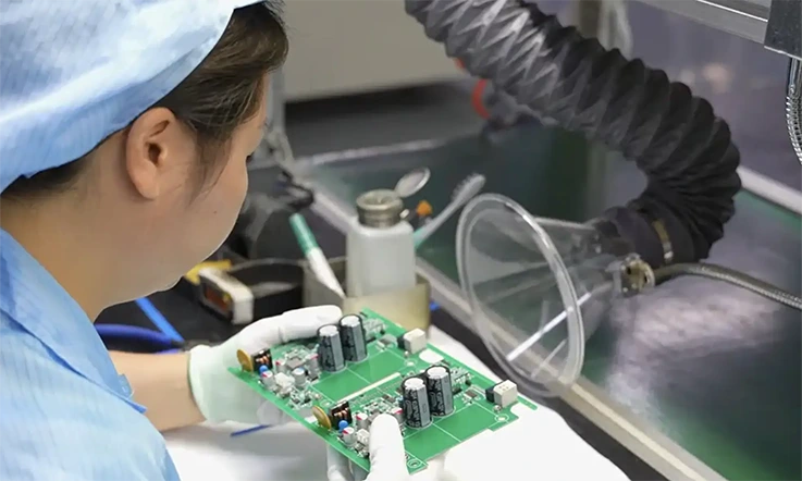
As the PCB manufacturing landscape continues to evolve, new technologies and manufacturing processes are dramatically shaping the way companies ensure product quality. From AI-driven inspection systems to the introduction of advanced materials like flex PCBs and HDI PCBs, the integration of these innovations into PCB quality assurance practices is setting the stage for a more efficient, accurate, and sustainable future. Below, we explore how emerging trends are redefining PCB quality management and pushing the boundaries of what’s possible in the industry.
The Role of Artificial Intelligence in PCB Inspection
Artificial Intelligence (AI) is rapidly making its mark in PCB manufacturing, offering groundbreaking advancements in automated inspection and defect detection. By incorporating machine learning algorithms into the inspection process, we can predict defects before they even occur, significantly improving the quality assurance process.
How AI is Revolutionizing PCB Inspection-
●Automated Defect Detection: Traditional methods of visual inspection are being replaced with AI-powered systems that can analyze images of PCBs in real-time to identify defects such as soldering errors, misalignments, and trace damage.
●Predictive Quality Control: AI algorithms analyze production data to predict areas most likely to develop defects, allowing us to implement corrective actions before problems arise. This is particularly useful in high-volume production, where human inspectors may miss subtle issues.
●Yield Optimization: By continuously learning from previous inspection data, AI models optimize production processes, reducing scrap rates and improving yield rates. AI can also adjust machine settings automatically to maintain consistency and reduce variability.
| Technology | Impact on PCB Quality | Benefits |
| AI in Inspection | Real-time defect detection, predictive defect analysis | Increased defect detection accuracy, reduced rework |
| Machine Learning | Optimizes production processes by analyzing data | Enhanced process efficiency, reduced downtime |
| Automated Defect Prediction | Prevents defects before they occur | Higher yield rates, better quality control |
AI in PCB manufacturing is also driving real-time data collection, making it easier for us to perform continuous process improvements. This capability allows us to meet the increasing demand for high-reliability PCBs with greater precision and fewer defects.
New Materials and Manufacturing Processes Shaping PCB Quality
The introduction of advanced materials and new manufacturing processes is significantly influencing PCB quality assurance. These innovations not only improve the performance and flexibility of PCBs but also bring about new challenges in terms of quality control and production techniques.
1.Flex PCBs, HDI PCBs, and 5G PCBs-
●Flex PCBs: These flexible printed circuits are gaining popularity due to their lightweight and adaptable nature, making them ideal for applications like wearables and mobile devices. However, ensuring consistent quality in flex PCB manufacturing requires specialized techniques to handle the bending and shaping of the circuits without damaging delicate components.
●HDI PCBs: High-Density Interconnect (HDI) PCBs allow for more complex circuits in a smaller footprint. However, HDI boards require fine-pitch components and microvias, making defect detection more challenging. Manufacturers must adopt high-precision techniques like laser drilling and automated optical inspection (AOI) to ensure quality.
●5G PCBs: As the demand for 5G technology increases, we must ensure that PCBs used in 5G devices meet strict signal integrity requirements. These boards must handle higher frequencies and more data, requiring advanced materials and fabrication techniques to prevent issues like signal loss, crosstalk, and interference.
2.Additive Manufacturing (3D Printing)-
●3D printing is making strides in PCB manufacturing by enabling rapid prototyping and customization. With 3D printing, manufacturers can produce complex geometries and integrate multi-materials in the PCB structure, opening up new possibilities for design and functionality.
●Material Innovation: The use of additive manufacturing is also driving new materials for PCBs, such as conductive inks and printed electronics, which offer more flexibility and reliability than traditional PCB materials.
| Technology/Material | Impact on PCB Quality | Challenges |
| Flex PCBs | Lightweight, adaptable, ideal for flexible electronics | Maintaining consistent quality during manufacturing |
| HDI PCBs | Smaller, denser circuits for complex designs | Difficulty in defect detection, fine-pitch components |
| 5G PCBs | High-speed, high-frequency performance for 5G tech | Signal integrity challenges, material complexity |
| Additive Manufacturing | Enables rapid prototyping and custom designs | New techniques required for consistent quality |
The shift towards flexible and high-density PCBs will likely continue to challenge quality assurance teams to adapt new inspection techniques and more precise manufacturing processes.
Automation and IoT for Smarter PCB Quality Assurance
The integration of Automation and the Internet of Things (IoT) into PCB manufacturing is reshaping the landscape of quality assurance. These technologies streamline processes, reduce human error, and provide real-time data, enabling smarter and more efficient production lines.
How IoT is Enhancing PCB Manufacturing-
●Real-Time Data Monitoring: IoT-enabled devices allow us to track every stage of the PCB manufacturing process, from assembly to inspection. Sensors and connected devices continuously monitor factors like temperature, humidity, and machine performance, ensuring optimal conditions for each step.
●Predictive Maintenance: Using IoT sensors to monitor machine performance can help predict equipment failures before they happen. This approach, known as predictive maintenance, reduces downtime and ensures consistent production quality. By avoiding sudden machine malfunctions, we can maintain high-quality standards throughout the entire production process.
●Smart Manufacturing: The integration of smart manufacturing systems enhances process automation, allowing for more precise control of production variables. Automated systems adjust machine settings based on real-time data, ensuring that manufacturing defects are minimized, and quality assurance processes are enhanced.
| Technology | Impact on PCB Quality | Benefits |
| IoT Devices | Real-time data collection and monitoring | Improved process control, reduced defects |
| Predictive Maintenance | Prevents unplanned downtime and machine failure | Increased machine uptime, better production consistency |
| Smart Manufacturing | Optimizes production processes based on data | Reduced human error, higher consistency |
Automation significantly reduces variability in PCB production by streamlining both assembly and testing processes. With robotic assembly lines and automated testing systems in place, human error is drastically minimized, ensuring that every board meets the highest standards. This leads to consistent, high-quality output with less downtime, which helps our clients keep pace with growing demand. Automated systems also enable faster production cycles, improving overall efficiency while maintaining rigorous quality control. As a result, we are able to consistently meet tight deadlines without compromising on the reliability or performance of the final product.
Why Choose Us Manufacturing Your PCB Circuit Boards?
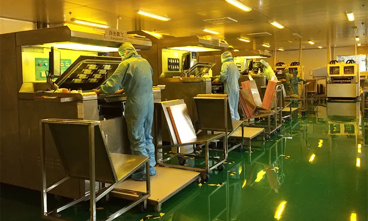
At JarnisTech, we take immense pride in delivering high-quality PCBs that meet your exact specifications, every time. Our PCB manufacturing and assembly services are designed to provide peace of mind through a rigorous quality control process, ensuring that each product is produced with precision and reliability. Whether you’re in need of rapid prototypes or custom-designed PCBs, our system guarantees that all products are made to the highest standards.
All PCBs Are Guaranteed To Be Manufactured to Your Specifications
Our approach to PCB assurance extends well beyond a mere promise written on paper. We implement a comprehensive system that ensures the manufacturing process is rigorously followed, from material procurement to the final inspection. Here’s how we maintain absolute control over your PCB production:
1.Clear Specification Documentation: We work with you to establish precise PCB design requirements, ensuring we understand every aspect of your project needs—whether it’s a custom trace layout, material selection, or layer count.
2.Defined Process Management: Each PCB undergoes a systematic flow from design verification, material sourcing, fabrication, and assembly. All steps are outlined and followed according to a strict quality assurance protocol.
3.Comprehensive Verification: Our process includes in-process inspections, automated testing (like AOI and X-ray inspection), and final testing to validate that the finished PCBs conform to your exact specifications.
This multi-layered approach assures that your PCB is manufactured within a clearly defined environment, minimizing risk and providing you with confidence that your boards will perform as expected from the first prototype to full-scale production.
| Step | Process Detail | Outcome |
| Specification Documentation | Detailed review of all customer requirements | Full alignment of design and production specs |
| Process Management | Defined workflow from sourcing materials to assembly | Controlled, repeatable production process |
| Verification | In-process inspections, automated testing, final QA checks | Assurance of conformance to specifications |
JarnisTech Manufactures PCBs Professionally at Competitive Prices
As a China-based PCB manufacturer, JarnisTech offers a full suite of PCB assembly and fabrication services at highly competitive prices. Whether you need quick-turn prototypes or large-volume production runs, we deliver a quality product without the hefty price tag. Here’s what makes our offerings stand out:
●Cost-Effective Manufacturing: By leveraging our advanced production facilities and streamlined supply chain, we are able to offer lower pricing compared to many other suppliers without sacrificing quality. Our location and process optimization allow us to pass on cost savings directly to you.
●Comprehensive PCB Solutions: We cover the entire PCB lifecycle, from design and prototyping to final assembly. Our factory handles all aspects of PCB manufacturing, so you don’t need to juggle multiple vendors.
●Global Standards Compliance: We ensure that all PCBs are manufactured to meet international standards, such as IPC-A-600 and ISO 9001, which guarantees consistent quality, reliability, and traceability.
Our 100% satisfaction guarantee means you can trust us to deliver exactly what you need, every time. If your order doesn’t meet your standards, we’ll work with you to make it right—no hassle, no headaches.
| Service | Detail | Benefit |
| Cost-Effective Production | Competitive pricing with no compromise on quality | Lower costs for high-quality products |
| Comprehensive Solutions | End-to-end PCB services from design to assembly | Seamless process with a single supplier |
| International Standards Compliance | Meeting global manufacturing standards | Assurance of high-quality, reliable PCBs |
PCB Quality Assurance FAQs
What types of PCB defects are typically found during quality assurance?
Common defects include open circuits, short circuits, soldering issues, misaligned components, and trace defects such as insufficient or excessive trace width.
How do you manage component placement accuracy in PCBs?
We rely on automated pick-and-place machines and perform in-circuit testing (ICT) to verify component placement, ensuring they meet the design specifications and are aligned correctly.
What testing methods do you use to verify PCB functionality?
We conduct electrical tests (such as ICT and boundary scan) to verify signal integrity and the functionality of the PCB, ensuring it operates as intended within its electrical limits.
How do you maintain PCB quality in high-volume production?
We apply statistical process control (SPC) to monitor the production process, continuously improving with real-time data analysis to maintain consistency and identify defects early.
What certifications should a PCB manufacturer have to ensure quality?
Look for certifications such as IPC-A-600 for visual inspection standards, ISO 9001 for quality management systems, and RoHS for environmental compliance, which guarantee adherence to industry standards.

