The journey from an abstract electronic concept to a tangible, high-performance device is one of immense complexity and precision. At the heart of this transformation lies the printed circuit board prototype. It is the physical manifestation of digital intent, the canvas where intricate circuit architecture meets the laws of material science and physics. A successful prototype is not a matter of chance; it is the outcome of a meticulously planned, holistic process where every variable, from the substrate’s dielectric constant to the micron-level accuracy of a laser-drilled via, is deliberately managed.
This guide navigates the complete lifecycle of prototype development. The exploration begins with the foundational principles of Design for Manufacturability (DFM) and the decisive task of material selection, establishing the groundwork for a robust and reliable build. From there, the discourse delves into core fabrication capabilities—exploring high-layer-count and HDI structures, complex via technologies, and the stringent quality assurance systems that verify their integrity. The narrative extends to integrated assembly, quick-turn solutions, and the economic factors at play. Ultimately, this document serves as a detailed map for engineers and innovators navigating the path to a flawless, production-ready design.
What is a PCB Prototype and Why is it Mission-Critical?
Before a design is committed to the vast expense and logistical scale of mass production, it must first prove its merit in the real world. A PCB prototype is that proof. It is a limited-quantity fabrication of a circuit board, produced not for the end market, but for the exacting scrutiny of its creators. Its existence allows engineers to hold their digital creation in their hands, to test its functions, and to uncover hidden flaws that no simulation could ever predict.
Defining the Prototype: More Than Just a Sample
A prototype transcends the definition of a simple “sample.” It is an engineering instrument, a tool for deep validation. Each one is purpose-built to answer specific questions about a design’s performance and manufacturability.
●An Engineering Instrument: Think of it as a high-fidelity model that allows for direct, empirical testing of electrical characteristics, mechanical fit, and thermal behavior. It moves the design from the theoretical realm of software into the physical domain.
●A Validation Checkpoint: The prototype serves to confirm that the layout integrity is sound, that components fit as intended, and that the chosen stack-up design performs under electrical load. It is the final checkpoint before committing to expensive production tooling.
●A De-Risking Mechanism: Identifying a design flaw at the prototype stage might cost hundreds or thousands of dollars to rectify through a board respin. Identifying that same flaw after a production run of ten thousand units could spell financial disaster and catastrophic project delays. The prototype is a powerful de-risking strategy.
The Core Purpose: Validating Your Design Before Mass Production
The fundamental objective of prototyping is verification. It provides tangible, measurable feedback on aspects of the design that are otherwise left to assumption. This verification process is multifaceted and addresses numerous design dimensions.
●Real-Time Performance Evaluation: It facilitates the direct assessment of trace routing, impedance path behavior, and signal phase alignment in high-speed or RF circuits. Issues like signal reflection, crosstalk, or unexpected attenuation become immediately apparent.
●Manufacturing Tolerance Checks: No manufacturing process is perfect. Variations in surface finish thickness, solder mask registration, and drill-to-pad accuracy can be measured on a prototype and refined before they impact yield in large-scale production.
●Material Interaction Testing: A prototype allows for stress-testing under controlled conditions. This can reveal potential issues like the thermal stability of dielectric layers during reflow soldering or the delamination risk in the flexible zones of a rigid-flex board.
●Physical Integrity Verification: It supplies clear feedback on panel warpage, bow, and twist, especially on boards with more than six layers or those using hybrid dielectric systems. Factors like copper distribution and stackup symmetry, which influence these mechanical properties, can be properly evaluated.
Key Prototype Types for Every Application
PCB prototype services accommodate a wide array of fabrication scenarios, each tailored to specific technical evaluations based on board structure, layer count, and signal requirements.
Comparison of Prototype Board Types:
| Type | Layer Count | Key Technologies | Applications |
| Single/Double Layer | 1–2 | Through-hole, basic SMT | LED drivers, power modules, sensors |
| Multilayer | 4–16+ | Blind/buried vias, plane layers | Routers, IoT gateways, FPGA boards |
| HDI | 4–10+ | Microvias, via-in-pad, laser vias | Smartphones, wearables, BGA-based designs |
| Flex / Rigid-Flex | 2–10+ | Polyimide, bend/fold zones | Aerospace, robotics, medical tools |
| RF / High-Speed | 2–12+ | Hybrid stackups, low-Dk materials | Radar, 5G, high-frequency comms |
●Single-Layer and Double-Layer PCBs: These are used for straightforward applications like simple power supplies, LED drivers, sensor modules, and basic analog controls. Their simplicity allows for exceptionally rapid turnarounds using standard FR-4 materials.
●Multilayer Boards (4–16+ Layers): These are deployed in designs where dense signal routing, complex power distribution networks, and electromagnetic interference (EMI) shielding are necessary. They provide dedicated ground and power planes, which are fundamental for signal integrity in digital and mixed-signal systems. Advanced techniques like blind and buried via drilling support their construction.
●High-Density Interconnect (HDI) Prototypes: Characterized by microvias, via-in-pad designs, and laser drilling, HDI boards are built for miniaturized electronics. Wearable devices, advanced medical sensors, and smartphone modules depend on this technology to accommodate fine-pitch components like BGAs and to reduce board size and weight.
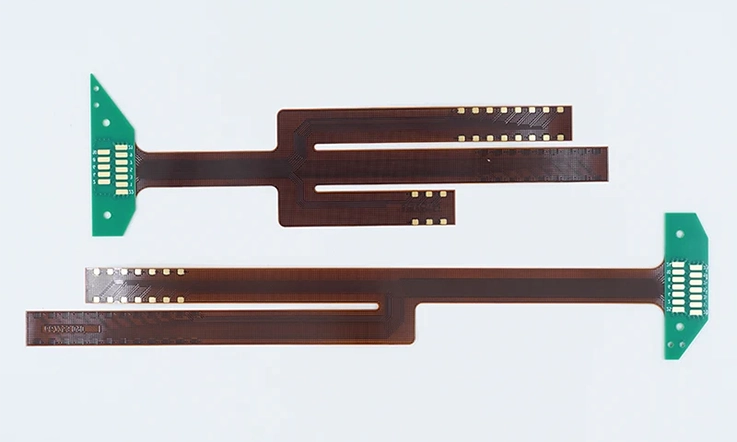
●Flex and Rigid-Flex Prototypes: These constructions combine dynamic, bendable sections with rigid, component-bearing sections in a single, integrated build. Manufactured with polyimide films, they are designed for applications requiring tight bend-radius compliance and three-dimensional assembly, such as in aerospace, robotics, and medical endoscopes.
●RF and High-Speed Prototypes: These prototypes often incorporate hybrid material stackups (e.g., FR-4 combined with Rogers or other low-loss dielectrics) to validate impedance matching and signal transmission in controlled dielectric zones. They are indispensable for developing telecommunications equipment, radar systems, and high-frequency data links.
The Foundation of Success: Design and Data Preparation
Predictable electrical performance and fabrication stability begin long before the first sheet of laminate is cut. They originate at the design stage. When working on prototypes—particularly those involving multilayer configurations, HDI layouts, or controlled impedance routing—details such as via approach, copper patterning, and stackup arrangement must reflect what the fabrication facility can support. A successful design is one that translates smoothly from the CAD tool to the physical board, respecting the realities of lamination, routing, and material processing.
Mastering DFM, DRC, and Stackup Optimization
Before sending a design out for fabrication, it should be reviewed against what the facility can handle to avoid process interruptions. . This involves preparing clear drill plans, balanced copper distribution, precise soldermask geometry, and accurate mechanical outlines.
●DFM (Design for Manufacturability):
This step focuses on confirming that the design details are compatible with current manufacturing capabilities.. This includes checking that trace widths and clearances meet the imaging system’s resolution, that BGA fanouts are achievable with the specified via technology (e.g., via-in-pad or microvia laser drilling), and that annular ring sizes are sufficient for the drill tolerances.
●DRC (Design Rule Check):
This automated check applies layer-specific spacing and width rules based on copper weight and prepreg characteristics. For boards with over six layers, special attention should be given to verifying through-hole annular rings and the clearances for anti-pads on internal planes. A well-configured DRC is the first line of defense against common fabrication defects.
●Stackup Definition:
For any impedance-controlled or RF design, the stackup must be precisely defined, specifying dielectric heights, prepreg types, and copper thicknesses. Using symmetrical stackups, where the layer sequence above the center is a mirror image of the sequence below, is a standard practice to reduce the risk of warpage during the high-temperature lamination process. For rigid-flex designs, defining adhesive layers and bending zone keep-outs early prevents fracturing and delamination issues.
Critical Layout Strategies for High-Speed, RF, and Impedance-Controlled Designs
For high-performance boards, maintaining a clean transmission path is fundamental to the design’s success. This extends beyond simple pad sizes and touches every aspect of the layout.
●Differential Pair Management: These pairs, used for high-speed data transmission, demand meticulous attention. The trace width and spacing must be kept uniform along the entire electrical path to maintain a constant differential impedance. Any deviations, copper voids on a reference plane, or stubs near trace transitions can introduce reflections and degrade signal integrity.
●RF Signal Zones: For frequencies extending above 1 GHz, layout practices become even more stringent. Using dedicated reference planes is a must, and maintaining clear, uninterrupted ground return paths directly beneath the signal traces minimizes inductance. Via stubs, the unused portion of a through-hole via, act as resonant antennas at high frequencies and must be avoided or removed through back-drilling.
●Copper Control and Balancing: Uniform copper fill should be used across all layers. This practice not only aids in preventing warpage but also ensures balanced plating thickness. Thinner outer layers can be over-etched, altering the final trace geometry and affecting impedance values. Copper thieving or patterning in sparse areas helps create a more uniform plating distribution.
●Flex and Rigid-Flex Specifics: The flexible sections of these boards introduce unique challenges. It is advisable to keep these areas free of impedance discontinuities by maintaining smooth, curved traces rather than sharp 90-degree bends. Differential pairs should be routed away from fold zones, and the transition from BGA escape routing on rigid sections to the microvia structures on the flexible interconnects must be designed to minimize stress.
Preparing Your Data Package: Gerber, BOM, and Beyond for Flawless Execution
Accurate design files are the bridge between your concept and a physical board. Supplying complete and aligned data is the single best way to ensure a smooth and error-free fabrication process.
●Gerber Files (RS-274X or X2): Confirm that layer alignment is perfect across all copper, mask, paste, and drill files. Board outlines should be closed polygons. For flex PCBs, the data package must include bend definitions, stiffener locations, and keepout zones on dedicated mechanical layers.
●Bill of Materials (BOM): For any project that includes assembly, a detailed and accurate BOM is indispensable. Providing exact manufacturer part numbers (MPNs), descriptions, and placement designators allows the assembly team to source the correct components and program pick-and-place machines without delay or ambiguity.
●Netlist or ODB++: Including a complete electrical netlist (in IPC-356 format) or a comprehensive data package like IPC-2581 or ODB++ helps the fabrication house perform advanced cross-checks. This allows them to compare the graphical Gerber data against the logical netlist to detect potential mismatches, opens, or shorts before production begins.
●Readme / Stackup Description: A simple plain-text readme file or a detailed PDF is invaluable. It should explicitly confirm the intended materials, copper weights for each layer, final board thickness, the desired surface finish, and any special instructions. This removes ambiguity and serves as a final specification check.
Material Selection: The DNA of Your PCB’s Performance
The substrate you choose for your PCB is a foundational decision that dictates its thermal, mechanical, and electrical behavior. While the copper layout determines the signal paths, a board’s durability during lamination, drilling, and assembly is governed by the underlying material. Each resin system interacts differently with processing heat and high-frequency signals. An improper material choice can introduce debilitating issues like delamination, excessive warpage, or signal performance degradation from the very start.
A Spectrum of Substrates: From Standard FR-4 to Advanced Laminates
A capable prototype service must accommodate a diverse range of substrates, as each material presents a unique profile of mechanical stability, thermal resilience, and electrical properties.
●FR-4 (Standard Epoxy Glass): A versatile and cost-effective choice, FR-4 is the industry workhorse for general-purpose multilayer boards. It performs well in most consumer and industrial test environments, with a thermal limit (Glass Transition Temperature, Tg) of around 130°C to 140°C.
●High-Tg FR-4: With a higher glass transition point (typically ≥170°C), this material offers enhanced thermal durability. It is well-suited for prototypes that will undergo the higher temperatures of lead-free assembly processes or for applications in demanding automotive or industrial systems where operating temperatures are elevated.
●Polyimide: Specified for high-heat applications in aerospace, defense, or power electronics, this substrate maintains its structural integrity at temperatures that can exceed 250°C. It provides excellent resistance to delamination and is the material of choice for most flexible and rigid-flex circuits, but it requires precise lamination process control.
●Rogers and PTFE-Based Materials: For high-frequency circuits where minimizing signal attenuation (low Dissipation Factor, Df) and maintaining a stable Dielectric Constant (Dk) are primary concerns, these low-loss dielectrics are the intended solution. They deliver stable performance for RF and microwave designs but require special handling during drilling and etching due to their softer, often ceramic-filled, resin content.
●Flex and Rigid-Flex Laminates: Built on polyimide films, these laminates allow circuits to bend and fold without fracturing. A successful design must carefully account for the properties of the coverlays, adhesives, and stiffeners to avoid creating brittle zones or compromising the circuit’s dynamic performance.
Common PCB Substrate Material Comparison:
| Material Type | Tg (°C) | Dk @ 1GHz | Df (Tanδ) | CTE (Z-axis ppm/°C) |
| FR-4 (Standard) | 130–140 | ~4.5 | 0.02–0.025 | ~220 |
| High-Tg FR-4 | ≥170 | ~4.3 | 0.015–0.020 | ~180 |
| Polyimide | >250 | ~4.2 | 0.01–0.015 | ~60–70 |
| Rogers 4350B | ~280 | 3.48 | 0.0037 | ~50 |
| PTFE (e.g., RT/duroid) | >300 | 2.2–2.6 | <0.001 | <30 |
| Flex Polyimide Laminates | >250 | 3.2–3.6 | 0.002–0.005 | ~12–30 |
Matching Material Properties to Your Application
Material selection goes deeper than just choosing by label. It involves examining detailed performance parameters and matching them to what the application requires in practice.
●Glass Transition Temperature (Tg): The temperature at which the material transitions from a rigid state to a softer, more pliable state. A higher Tg indicates better thermal stability. High-Tg FR-4 is recommended for boards that will experience multiple soldering cycles, thermal shock, or high-temperature operation. Standard Tg FR-4 is suitable for low-speed digital circuits or power boards where thermal stress is not a design driver.
●Dielectric Constant (Dk): This property affects signal propagation speed and impedance. For high-speed designs, a lower Dk is often desirable. Even more so, the stability of the Dk across a range of frequencies is a defining characteristic of high-performance materials. Rogers or Taconic materials are engineered for stable Dk in circuits operating above 2 GHz or where phase stability is a requirement.
●Dissipation Factor (Df or Tanδ): This measures how much signal energy is lost as heat within the dielectric. A lower Df is indispensable for maintaining signal integrity in very high-frequency or long-trace applications. Materials like PTFE and advanced ceramics offer exceptionally low Df values.
●Coefficient of Thermal Expansion (CTE): This measures how much the material expands when heated. A lower CTE, particularly in the Z-axis, is desirable to reduce stress on plated through-holes during thermal cycling, which can lead to barrel cracking and reliability failures. Polyimide and some advanced composites offer superior CTE performance compared to standard FR-4.
Performance Properties and Application Guidelines:
| Property | Ideal Value Range | Material Examples | Best Suited Applications |
| Tg (Glass Transition) | 170–250+ °C | High-Tg FR-4, Polyimide | Lead-free soldering, high-temp environments |
| Dk (Dielectric Constant) | 2.2–3.5 (stable range) | Rogers 4000 series, PTFE | RF, microwave, high-speed digital |
| Df (Dissipation Factor) | <0.005 | PTFE, Rogers 3000 series | GHz-range signal paths, low-loss data transmission |
| CTE (Z-axis) | <70 ppm/°C | Polyimide, ceramic hybrids | High-reliability multilayer and flex designs |
Balancing Performance, Cost, and Manufacturability
The material selection process is an exercise in engineering trade-offs. It directly affects prototype cost, manufacturing yield, and lead time. An reliable choice requires balancing several practical factors.
●Cost and Availability: PTFE and ceramic-filled laminates offer superior electrical properties but often come with longer lead times and significantly higher material costs. Polyimide substrates are typically more expensive than FR-4 but can reduce the risk of failure in complex, multi-lamination builds. Checking your supplier’s in-stock list for your chosen materials is a simple step that can prevent unexpected project delays.
●Manufacturing Considerations: The chemical and mechanical compatibility of adhesive and prepreg layers in rigid-flex stackups is fundamental to preventing warping or delamination. Drilling high aspect ratio holes is more challenging in some softer materials than in FR-4; thicker specialty laminates may require different processing steps, such as peck drilling or laser ablation.
Core Manufacturing Capabilities: Where Precision Engineering Comes to Life
Delivering a precision circuit board requires more than just an accurate layout file; it demands a synergy of advanced machinery, engineering expertise, and tightly controlled processes. A capable prototyping facility must navigate high-layer counts, ultra-thin cores, and complex via architectures while holding strict mechanical tolerances. For today’s consumer electronics, medical devices, and telecom modules, manufacturing advanced structures like rigid-flex boards or HDI with stacked microvias is a baseline capability.
Multilayer, HDI, and Rigid-Flex: Building Complexity with Confidence
While many prototypes start as multilayer boards, advanced applications require capabilities that go far beyond simple layering.
●Multilayer PCB Builds (up to 36 layers): These constructions enable dense routing for complex, high-pin-count components like FPGAs and BGAs. Success depends on stable lamination under immense pressure and heat, a symmetrical stackup to prevent warpage, and precise layer-to-layer registration (often within ±50µm) to ensure that drilled holes correctly intersect their target pads on all inner layers.
●HDI PCB Support: This technology, defined by IPC-2226, includes laser-drilled microvias, stacked or staggered via-in-pad designs, and sequential lamination. These techniques allow for much tighter component placement, shrinking board size while effectively isolating signals for high-speed components like CPUs and memory controllers. An HDI build may involve multiple lamination cycles, adding complexity to the process.
●Rigid-Flex PCB Construction: These designs seamlessly blend the stability of rigid FR-4 sections with the versatility of flexible polyimide layers. Special attention is given to bond-ply adhesion, defining precise bend radii to prevent trace cracking, and aligning coverlays to protect exposed circuitry without compromising flexibility. The transition zone between the rigid and flex sections is a point of high mechanical stress and requires careful design and process control.
Advanced Via Structures: Blind, Buried, Stacked, and Microvias
The ability to implement complex via configurations directly impacts a board’s routing density, potential for miniaturization, and signal integrity.
●Blind Vias: Connecting an outer layer to one or more inner layers, these vias free up valuable routing space on dense boards without passing through the entire structure. The precision of the depth-controlled mechanical drill or laser drill, along with the subsequent plating process, is foundational to their reliability.
●Buried Vias: These connect only inner layers, leaving the outer surfaces completely uninterrupted for component placement in HDI designs. Proper resin fill and a thorough desmear process (to remove drill debris and resin smear from the inner-layer copper) during fabrication are necessary to prevent voids or open circuits.
●Microvias: Typically formed with UV or CO2 lasers and measuring less than 150µm (6 mils) in diameter, these are necessary for the fine-pitch BGA packages found in modern smartphones and IoT modules. Their formation requires precise laser depth control to ensure a dependable electrical connection to the target pad without damaging underlying layers.
●Stacked Vias: In the most advanced HDI designs, microvias can be stacked on top of each other through multiple layers (e.g., a microvia from layer 1-2 is stacked on a microvia from layer 2-3). This requires multiple sequential lamination and plating cycles and represents a pinnacle of fabrication capability, demanding exceptional process control to ensure a continuous, reliable connection through the stack.
The Art of Precision: Drilling, Etching, and Soldermask Application
The difference between a functional prototype and one that fails often lies in microscopic fabrication details that are invisible to the naked eye.
●Drilling Systems: A combination of high-speed mechanical drilling and high-precision laser drilling is used to create everything from large mounting holes to sub-100µm microvias. The quality of the hole wall, the positional accuracy of the drill hit (registration), and the integrity of the subsequent via metallization process all contribute to the final board’s connectivity and long-term reliability.
●Etching Precision: This process directly defines the final geometry of impedance-controlled traces. High-resolution direct imaging (LDI) and carefully controlled chemical etching processes are used to produce clean, straight trace sidewalls and meet tight width and spacing requirements, sometimes down to 2-3 mils.
●Soldermask Application: Far more than just a colored coating, the LPI (Liquid Photoimageable) soldermask is fundamental for high-yield automated assembly. Precise registration of the soldermask dam between fine-pitch pads prevents solder bridging during reflow and ensures that BGA balls make proper contact with their pads, directly impacting the success of the assembly stage.
Turnkey Solutions: Integrating PCB Assembly (PCBA) for Speed and Efficiency
A bare, unpopulated circuit board is only a partial solution. To truly validate a design, it needs to be assembled with its intended components and tested as a functional system. By integrating professional PCB assembly (PCBA) into the prototype phase, you receive a board that is ready for immediate power-up, testing, and firmware validation. This streamlined, single-source approach eliminates logistical headaches and accelerates the entire development timeline.
Why a Single-Source Partner for Fabrication and Assembly Matters?
Coordinating between a separate fabrication house and an assembly provider introduces complexity, potential for miscommunication, and delays. A single-source, turnkey solution offers compelling advantages.
●Elimination of Logistical Bottlenecks: There is no need to ship bare boards from one facility to another, saving valuable time and shipping costs. This also removes the risk of boards being damaged in transit between vendors.
●Seamless Data Transfer: The same engineering team that validates your Gerber files for fabrication can use your BOM and centroid data for assembly. This ensures perfect alignment between the physical board and the assembly program, reducing the risk of component placement errors.
●Accountability and Problem Solving: If an issue arises, there is a single point of contact. There is no finger-pointing between a board fabricator and an assembler regarding issues like pad solderability or dimensional inaccuracies. Problems are identified and solved efficiently under one roof.
●Accelerated Timelines: The transition from the final step of bare board fabrication (e.g., electrical testing) to the first step of assembly (solder paste printing) can happen in minutes, not days. This compressed schedule is a massive benefit for projects with aggressive deadlines.
Our PCBA Capabilities: SMT, THT, and BGA Expertise
A comprehensive assembly service must be equipped to handle the full range of modern electronic components, from tiny surface-mount devices to large through-hole connectors.
●Surface-Mount Technology (SMT): High-speed, automated pick-and-place machines accurately place a vast array of components, from small 0201 or 01005 passive components to large, high-pin-count Quad Flat Packages (QFPs) and Ball Grid Arrays (BGAs). Precise solder paste application and carefully controlled multi-zone reflow ovens are used to create reliable solder joints.
●Through-Hole Technology (THT): While SMT dominates modern electronics, THT components like connectors, large capacitors, and power transistors are still common for applications requiring mechanical strength. Both manual soldering by skilled technicians and automated selective soldering processes can be employed to ensure robust connections.
●BGA and Fine-Pitch Placement: Placing and soldering BGAs, where the connections are hidden underneath the component package, demands exceptional precision. Automated 3D X-ray inspection (AXI) is used after reflow to inspect the solder joints for voids, shorts, and proper formation, guaranteeing the integrity of these complex connections.
From BOM Scrubbing to Component Sourcing: A Seamless Process
A significant portion of a project’s timeline can be consumed by issues with the Bill of Materials (BOM) and component availability. Proactive management of the supply chain is a hallmark of a mature turnkey service.
●BOM Analysis and Scrubbing: Before any parts are ordered, the BOM is “scrubbed” by a procurement specialist. This involves verifying manufacturer part numbers (MPNs), checking component footprints against the PCB layout, identifying potential long-lead-time or obsolete parts, and suggesting suitable alternatives.
●Component Sourcing: Leveraging established relationships with a global network of authorized distributors, the service can source high-quality, authentic components efficiently. This mitigates the risk of receiving counterfeit parts, which can cause catastrophic field failures. For quick-turn prototypes, having an in-house stock of common passive components can further accelerate the process.
●Kitted vs. Turnkey: You have the flexibility to either supply the components yourself (a “kitted” assembly) or have the provider handle all procurement (a “full turnkey” assembly). Full turnkey is the most streamlined option, offloading the entire sourcing and logistics burden from your engineering team.
The Result: A Functional, Test-Ready Board, Faster
The ultimate outcome of an integrated turnkey service is speed and confidence. You receive a fully assembled prototype, often inspected and even functionally tested if requested, that is ready for your engineers to begin the work they do best: developing firmware, validating system performance, and pushing the project forward to the next milestone. This transforms the prototype from a collection of parts into a working piece of hardware in the shortest possible time.
Quality Assurance as a Standard, Not an Option
A precision-built prototype demands measurable and verifiable quality. From copper integrity and via continuity to high-voltage insulation, quality cannot be an assumption; it must be engineered into every step of the process. This is achieved through a robust system of standards, inspections, and repeatable process controls that are integral to the fabrication capabilities. These benchmarks aren’t just labels—they reflect the documented processes behind every panel that is pressed, drilled, and plated.
Adherence to Industry Standards: IPC Class 2/3, ISO 9001, and UL
The foundation for dependable output begins with adherence to traceable industry frameworks. When developing prototypes for use in telecommunications, medical, or industrial environments, the baseline quality levels must reflect the realities and pressures of operational conditions.
●IPC Class 2 and Class 3 Compliance: Fabrication can be offered to meet the stringent requirements of these IPC standards. IPC Class 2 is the standard for most commercial electronics. IPC Class 3, required for high-reliability applications like aerospace and life-support medical devices, imposes much tighter tolerances on aspects like annular ring integrity (minimum breakout is not allowed), solder mask alignment, hole wall plating quality, and plated via aspect ratios.
●ISO 9001 Certified Quality System: An ISO 9001 certification ensures that documented, process-level procedures are followed across all lamination, drilling, and final inspection workflows. This commitment to process control delivers consistent and traceable results from one order to the next.
●UL Recognition: The use of UL-recognized materials with certified flammability classes (like 94V-0) is available to support products that require high-temperature operation and verified dielectric strength for safety compliance.
Rigorous Inspection and Testing: AOI, Flying Probe, and ICT
The inspection protocol should combine advanced imaging with real-time electrical validation. While optical inspection confirms physical geometry, only direct electrical testing can guarantee via continuity, net isolation, and freedom from opens or shorts.
●Automated Optical Inspection (AOI): Performed on every layer, including the inner cores before lamination. AOI systems use high-resolution cameras to compare the etched layer against the original Gerber data, verifying trace continuity, layer registration, and fine-pitch etching quality.
●Flying Probe and E-Test Fixtures: These systems perform 100% electrical checking on every net of the bare board. A “flying probe” tester uses two or more robotic probes to move from pad to pad, checking for continuity between all points on a net and for isolation from all other nets. This ensures all connections match the netlist perfectly.
●In-Circuit Test (ICT) Support: For assembled prototypes, support for ICT fixture development can be provided. This allows for the verification of component-level electrical performance after parts are soldered, confirming that the board functions as intended.
●Time-Domain Reflectometry (TDR): For impedance-controlled boards, TDR measurements are performed on test coupons fabricated on the same panel as the boards. This test sends a high-speed pulse down a trace and measures the reflections, providing a precise, real-world measurement of the trace’s characteristic impedance.
Full Traceability and Compliance: Your Guarantee of Quality
For every prototype run, the ability to trace materials, process cycles, and test results provides transparency and verification. This commitment to compliance is a baseline for trust.
●RoHS-Compliant Builds: Full support for lead-free manufacturing is a modern necessity. This includes using standard and high-Tg cores that are compatible with lead-free processes and offering compliant surface finishes like lead-free HASL, ENIG, and immersion silver.
●Full Traceability: Traceability coding, including panel numbers, inner layer registration codes, or laser-engraved unique board IDs, can be implemented where specified. This allows every board to be traced back to its specific production lot and material batches.
●Process Records and Controlled Environments: Lot-linked press and imaging records should be retained, providing valuable data for future production runs or comparative analysis. Cleanroom processes and anti-static handling are employed for sensitive designs that have low contamination or specialty dielectric requirements. This level of documentation provides full transparency and ensures process reproducibility.
From Board to System: Troubleshooting Common Prototype-Level Failures
Even the most carefully designed prototype can present unexpected challenges during validation. Identifying the root cause of a failure—whether it lies in the design, the materials, or the fabrication process—is a defining skill for an engineer. A high-caliber prototyping service acts as a technical ally in this process. Understanding common failure modes provides a framework for diagnosing issues quickly and preventing them in future design iterations.
Diagnosing Electrical Performance Issues
These are often the most complex failures, manifesting as poor signal integrity, incorrect timing, or outright functional failure.
1.Impedance Mismatch:
●Symptom: High signal reflection, ringing, or poor eye diagrams in high-speed nets.
●Potential Causes: Deviation in trace width or dielectric height from the design specification; incorrect material (Dk) used; unexpected variations in copper thickness after plating.
●Diagnosis & Solution: Use a Time-Domain Reflectometer (TDR) on test coupons from the same panel to measure actual impedance. The solution involves a tight feedback loop with the fabrication house to adjust the stackup model based on their specific process capabilities, ensuring the final product matches the simulation.
2.Excessive Crosstalk:
●Symptom: Unwanted noise induced on a quiet trace from a nearby switching trace.
●Potential Causes: Traces routed too closely together for too long a distance; inadequate reference plane causing a wide field projection.
●Diagnosis & Solution: Analyze nets with an oscilloscope. In the design, increase spacing between aggressive nets, decrease the dielectric height to a closer reference plane, or use guard traces. A prototyping house can offer DFM feedback on routing density to flag high-risk areas.
3.Power Delivery Network (PDN) Noise:
●Symptom: Unstable voltage rails, jitter in high-speed clocks, or random logic errors.
●Potential Causes: Insufficient decoupling capacitance, poorly designed power planes (e.g., split planes creating long return paths), high plane inductance.
●Diagnosis & Solution: Measure rail noise with a high-bandwidth oscilloscope. The design fix involves adding more decoupling capacitors closer to the IC power pins and ensuring solid, continuous power and ground planes.
Identifying and Preventing Mechanical Failures
These failures relate to the physical structure of the board and its ability to withstand thermal and mechanical stress.
1.Delamination or Blistering:
●Symptom: Layers of the board separating or forming bubbles, typically after reflow soldering.
●Potential Causes: Trapped moisture within the laminate; an improper lamination cycle (incorrect pressure or temperature profile); significant CTE mismatch between materials in a hybrid stackup.
●Diagnosis & Solution: Visual inspection, often after thermal stress. Prevention is design- and process-based: ensure the fabrication house bakes materials to remove moisture before lamination, use symmetrical stackups to balance stress, and select materials with compatible CTEs.
2.Via Reliability Failures (Barrel Cracking):
●Symptom: Intermittent or total open circuits in a plated through-hole, especially after thermal cycling.
●Potential Causes: High Z-axis CTE of the material places stress on the plated copper barrel; poor quality or insufficient thickness of the copper plating.
●Diagnosis & Solution: Cross-sectioning (micro-sectioning) the via to visually inspect for cracks. To prevent this, select low Z-axis CTE materials, and ensure the fabrication process uses high-ductility copper plating and adheres to IPC Class 3 standards for plating thickness.
3.Pad Cratering or Lifting:
●Symptom: A pad lifts off the surface of the PCB, sometimes taking a chunk of the laminate with it (cratering).
●Potential Causes: Mechanical stress during assembly or rework, often exacerbated by the brittleness of some lead-free solder alloys.
●Diagnosis & Solution: Visual inspection under magnification. Design-level prevention includes using non-soldermask defined (NSMD) pads for BGAs, which are less prone to stress concentration, and ensuring via-in-pad structures are properly filled and plated to avoid weakness.
Mitigating Common Assembly Defects
These issues arise when components are soldered to the prototype board, often pointing to an interaction between the board finish, component type, and assembly process.
1.BGA Soldering Faults (Voids, Head-in-Pillow):
●Symptom: Open connections or unreliable performance from a BGA component.
●Potential Causes: The “head-in-pillow” defect occurs when the solder ball and solder paste melt but fail to coalesce, often due to board warpage. Voids are gas bubbles trapped in the joint.
●Diagnosis & Solution: Automated X-ray Inspection (AXI) is the only way to see these defects. Prevention includes using a highly planar surface finish like ENIG, controlling board warpage through symmetrical design, and using an assembly provider who can create an optimized reflow profile for the specific board and components.
2.Solder Bridging:
●Symptom: An unwanted electrical short between two adjacent pads.
●Potential Causes: Inaccurate solder paste stencil printing; poor registration of the soldermask, leaving an insufficient soldermask dam between pads.
●Diagnosis & Solution: Visual inspection or electrical test. This is almost always a process- or fabrication-level issue. A high-quality prototype will have precise soldermask registration, and a good assembly process will use 3D solder paste inspection (SPI) to verify paste deposits before component placement.
Meeting Your Deadlines: Our Quick-Turn Prototyping Services
When hardware validation windows are tight, accelerated prototyping services can make the difference between project momentum and costly delays. A rapid fabrication process can deliver complex stackups and diverse materials with precise layer registration, all while maintaining the integrity of your design intent. This focus on controlled speed enables you to get functional boards into the hands of your engineers faster, allowing for earlier debugging and more confident project decisions.
Express Fabrication: From 24-Hour Builds to Complex Multilayers
High-speed and multilayer designs can be fabricated within compressed timeframes, often in one to two working days, provided that the design files are fully verified and the specified materials are in stock.
●24-hour and 48-hour services are typically offered for double-sided, 4-layer, and select 6-layer designs that can leverage standardized production cycles and materials.
●Boards with up to 20 layers can be produced within 72 hours or slightly more when using in-stock laminates like high-Tg FR-4.
●The quick-turn process utilizes pre-configured tooling templates for inner layer imaging, lamination press programs, and drilling routines, which minimizes setup delays between jobs.
●Even on these accelerated timelines, strict process control for impedance-sensitive and RF-compatible prototypes is maintained, including all standard quality checks. Fast delivery does not mean a reduction in standards.
Quick-Turn Fabrication Timeframes by Board Complexity:
| Board Type | Typical Layers | Turnaround Time | Material Availability Requirement |
| Double-sided FR-4 | 2 | 24–48 hours | Standard FR-4, 1oz Cu |
| 4-layer standard board | 4 | 48 hours | Standard FR-4, high-Tg optional |
| 6-layer digital board | 6 | 48–72 hours | In-stock high-Tg FR-4 |
| 8–12 layer prototype | 8–12 | 3–4 working days | Pre-stocked materials preferred |
| HDI / RF / hybrid stackup | 8–20+ | 4–7 working days | Rogers/PTFE may require longer lead time |
How Speed is Achieved Without Sacrificing Quality?
Accelerated builds are not the result of cutting corners. They are the product of a fine-tuned and highly efficient manufacturing logic that prioritizes workflow and minimizes idle time.
●Process Optimization: Quick-turn lines are often dedicated and optimized for high-mix, low-volume work. This means machine setups are streamlined, and the flow from one station (e.g., drilling) to the next (e.g., plating) is designed for maximum velocity.
●Digital Integration: A fully digital front-end process, from quoting to CAM tooling, allows a verified design to enter the fabrication queue almost instantly. There are no manual data entry or conversion delays.
●Maintained Quality Checks: All standard quality verifications, such as AOI scanning of inner layers, X-ray inspection for layer alignment, and final flying probe electrical testing, remain integral parts of the quick-turn process. The speed comes from efficiency, not from omission.
Balancing Speed, Cost, and Complexity: Making the Right Choice
While rapid turnarounds offer a clear advantage in a development race, balancing speed with cost and board complexity is a mark of sound engineering judgment. Here are some practical tips for optimizing a quick-turn order.
●Use Standard Board Sizes and Common Materials: Designs that use common materials (like 1.6mm FR-4 with 1oz copper) and fit efficiently onto standard production panels can be routed through the most efficient production paths.
●Avoid Non-Essential Complex Features: Features like blind/buried vias or multiple lamination cycles add manufacturing steps and time. Unless they are absolutely necessary for the prototype’s function, omitting them can significantly speed up the build.
●Align with Quick-Turn DFM Standards: Adhering to slightly more generous design rules for trace/space widths, via aspect ratios, and ensuring balanced copper distribution can allow the design to proceed without holds or engineering questions.
●Factor in the Premium: Rush builds naturally command a premium price because they require dedicated machine time and often disrupt the standard production schedule. This premium increases with board complexity (e.g., for designs involving microvias or sequential lamination). Evaluating these trade-offs upfront allows you to leverage the benefits of speed while ensuring the performance and reliability of your prototype.
Speed-Cost-Complexity Trade-off Matrix:
| Factor | Low Complexity Build | Moderate Complexity Build | High Complexity (HDI, RF, etc.) |
| Standard Turnaround Time | 2–3 days | 3–5 days | 5–7+ days |
| Rush Fee Premium (Estimate) | +20–30% | +40–60% | +80–150% |
| Typical Design Rule Tolerance | 6/6 mil trace/space | 4/4 mil or finer | ≤3/3 mil, microvias |
| Preferred Material | FR-4 (1.6mm, 1oz Cu) | High-Tg FR-4, basic polyimide | PTFE, Rogers, hybrid stackups |
Understanding the Investment: Key Cost Drivers in PCB Prototyping
Understanding what drives the cost of a PCB prototype gives you far more control than simply comparing final quotes. In circuit board fabrication, every design parameter—from the layer stack to the board’s outline—influences the manufacturing route, tooling setup, and material usage. Recognizing these variables is a matter of design intelligence, allowing you to find cost efficiencies without compromising performance or reliability.
How Layer Count, Materials, and Finish Impact Your Budget?
Boards with higher layer counts, specialized materials, or advanced surface finishes require more manufacturing steps and tighter process controls, which in turn affects the final cost.
●Layer Count: The relationship between layer count and cost is not linear; it is exponential. Builds with two or four layers generally use simpler, single-step lamination setups. Designs with six or more layers often require more complex pressing cycles, and HDI designs with blind/buried vias demand multiple sequential lamination steps, each adding significant time and process risk.
●Material Type: FR-4 serves as the cost-effective baseline. High-TG and polyimide materials command a higher price due to the raw material cost and the longer, more controlled lamination cycles they require. Low-loss substrates like Rogers or Megtron are specialty materials that involve higher costs and specialized handling and surface preparation logistics.
●Surface Finish: Lead-free HASL is a common, cost-effective option but offers less surface planarity. Finishes like ENIG or immersion silver provide a flatter surface that is better for fine-pitch components but involve additional chemical processing steps and precious metals, increasing the price.
The Economics of Panelization and Order Size
How an individual board design fits onto a large fabrication panel directly impacts material waste and the per-unit cost. Even a well-designed circuit can be inefficient to produce if its layout is not optimized for standard panel formats.
●Panel Utilization: Fabrication facilities process large panels of material (e.g., 18″ x 24″). The number of your boards that can fit onto one of these panels determines the material efficiency. Designs with regular, rectangular shapes that can be tightly nested on a panel result in less wasted material and lower per-unit costs.
●Order Volume: Low-quantity builds carry a higher per-unit cost because the one-time setup charges (NRE – Non-Recurring Engineering) for tooling and programming are amortized over fewer pieces. Mid-size batches (e.g., 50–500 units) typically offer a much better cost-to-volume ratio as the NRE becomes a smaller fraction of the total cost.
●Depanelization Method: The method used to separate individual boards from the panel also affects cost. Straight-line V-scoring is generally the most material-efficient and fastest method. Tab-routing, which leaves small tabs connecting the board to the panel frame, requires additional CNC machine time and introduces more waste material.
The Value Proposition: Domestic vs. Offshore Prototyping
While geography influences prototype budgeting, the decision involves more than labor rates. The modern trade-off balances lead time, logistics, and the quality of engineering communication against the base unit price.
1.Local (Domestic) Fabrication Benefits:
●Benefit from faster and more predictable cycle times for urgent design validation.
●Enjoy easier, real-time communication in the same time zone for any design clarifications or adjustments.
●Avoid potential international shipping delays, customs uncertainties, and tariffs.
●Often provides a higher degree of intellectual property (IP) protection.
2.Offshore Fabrication Considerations:
●May present a lower unit price, especially for high-volume or low-complexity boards where labor is a larger cost component.
●Carries the risk of extended delivery times and less flexibility for mid-production changes due to time zone and language barriers.
●Requires thorough verification of material standards and process control capabilities to ensure you are not receiving substandard or counterfeit materials.
For rapid design sprints or complex prototypes requiring close collaboration, domestic production often provides a total value that offsets the price difference. For simpler, high-volume builds where timelines are flexible, offshore production can be a viable option.
Getting Started: Our Streamlined Ordering and Production Workflow
Moving a PCB prototype from concept to shipment is a structured, traceable process. This section outlines a workflow designed to translate your design into a physical board with precision and transparency at every stage. A well-defined process ensures the integrity of every lamination, via, and trace, resulting in a reliable, high-quality prototype.
Step 1: Secure File Submission and Online Quoting
The process begins when you provide a complete and accurate design package. Modern online quoting tools are designed to translate your specifications into an accurate quote while validating key parameters in real-time.
A complete package for a turnkey fabrication and assembly project includes:
●Gerber files (RS-274X or X2) for all copper, soldermask, silkscreen, and paste layers.
●Drill files (Excellon format) with tool sizes and locations clearly defined.
●A stackup drawing indicating materials, thicknesses, and copper weights for each layer.
●A detailed Bill of Materials (BOM) for component sourcing.
●Centroid (XY placement) data for automated assembly machines.
An advanced online quoting system provides:
●Real-time price adjustments for different quantities, layer counts, materials, and finishes.
●Accurate impedance modeling for various high-speed materials.
●Automatic recognition of advanced structures like blind/buried vias to correctly calculate the required number of lamination cycles.
Step 2: In-Depth Engineering Review and CAM Approval
Once an order is placed, an engineering team begins a detailed manufacturing review. This CAM (Computer-Aided Manufacturing) validation ensures your design is fully compatible with the chosen fabrication processes, especially for complex, high-density builds.
Key Engineering Checkpoints:
●Verifying minimum annular ring against drill tolerances to ensure via reliability.
●Correlating copper thickness to the required trace width precision after etching.
●Checking for copper plane balance across the stackup to prevent board warpage during lamination.
●Optimizing drill paths and tool selections to reduce machine time and ensure excellent hole quality.
Final CAM approval signifies that your digital design is fully verified and ready for physical production. This step confirms that all tolerances can be met and potential manufacturing issues have been proactively resolved.
Step 3: Transparent Production, Tracking, and Post-Delivery Support
The final stage is to ensure your valuable prototypes are protected during transit and supported after delivery.
Professional Packaging and Logistics:
●All boards are vacuum-sealed in ESD-safe packaging to prevent oxidation and static damage.
●Boards are protected with rigid edge guards or custom foam during transit to prevent mechanical shock.
●Shipments include full tracking information from major carriers like FedEx, UPS, or DHL.
Documentation and Post-Delivery Support:
●Batch-specific documentation can be provided upon request, such as impedance test coupons, board thickness verification reports, or Certificates of Conformance.
●Each board can be marked with a scannable ID for full traceability back to its production lot.
●A technical team should be available to answer any questions regarding the fabrication or assembly of your delivered prototypes.
Why Choose JarnisTech for Your PCB Prototype Manufacturing Services?
Selecting a fabrication and assembly house is a defining decision for any engineering project. It’s a choice that extends beyond a simple transaction; it’s about entrusting your innovation to a capable steward. At JarnisTech, we understand this responsibility. Our entire operation is built around delivering not just a physical product, but also confidence, predictability, and technical excellence.
Uncompromising Quality as a Baseline
Quality at JarnisTech is not a feature to be inspected at the end of the line; it is engineered into every step of our process. It begins with sourcing premium raw materials from globally recognized suppliers and is maintained through a rigorously documented, ISO 9001 certified quality management system. We offer fabrication that meets the demanding criteria of IPC Class 2 and Class 3, ensuring that every via, trace, and pad conforms to the highest standards of reliability. Through advanced inspection methodologies like Automated Optical Inspection (AOI) on every layer and 100% electrical flying probe testing, we ensure that the board you receive is an exact, flawless representation of your design.
Optimized Cost-Effectiveness, Not Just a Low Price
True value is found in the balance between cost and outcome. Our approach focuses on delivering superior cost-effectiveness by optimizing every aspect of the manufacturing process. Through intelligent panelization algorithms, we maximize material utilization to reduce waste. Our proactive DFM engineering support identifies and resolves potential manufacturability issues before they lead to costly respins and delays. By offering integrated, turnkey assembly services, we eliminate the hidden costs and logistical friction of coordinating with multiple vendors. The price you are quoted reflects a streamlined, efficient process designed to deliver a successful outcome on the first pass.
Predictable and Expedited Delivery
In today’s development cycles, time is a non-renewable resource. Our operational model is built for speed and predictability. For standard specifications, our quick-turn services can deliver high-quality prototypes in as little as 24 hours. This velocity is not achieved by cutting corners, but by a highly integrated digital workflow, optimized production scheduling, and dedicated high-mix manufacturing lines. From instant online quoting to real-time order tracking, you maintain full visibility throughout the process, ensuring your project timelines are met with confidence.
Service Grounded in Engineering Expertise
We view every project as a technical collaboration. Our service extends far beyond order taking. It is delivered by a team of experienced engineers who speak your language. When you submit a design, it undergoes a thorough DFM review to identify potential risks and opportunities for optimization. If you are navigating complex challenges like impedance control, hybrid stackups, or via-in-pad designs, our specialists are available to provide expert consultation. This collaborative approach ensures that potential problems are solved proactively, saving you invaluable time and resources.
Advanced Capabilities to Realize Ambitious Designs
Your most ambitious designs require a fabrication house with equally ambitious capabilities. JarnisTech is equipped to bring complex electronic concepts to life. Our expertise spans high-layer-count multilayer boards, intricate HDI structures with stacked microvias, and challenging rigid-flex constructions. We handle a wide spectrum of advanced materials, from high-frequency RF laminates to robust high-Tg substrates suitable for extreme environments. Whether your design demands laser drilling, back-drilling, heavy copper, or adherence to the strictest industry certifications, our facility has the technology and the expertise to execute it with precision.
Your next innovation is ready to take physical form. Begin the process by uploading your files to receive an instant, detailed quote for your prototyping and assembly needs.
FAQ & PCB Prototype Services
1.How does HDI PCB prototyping help with complex designs?
HDI offers higher density and smaller designs, perfect for compact, complex applications.
2.How does customer support improve PCB prototyping?
It ensures guidance and quick solutions throughout the design and prototyping process.
3.Why should I choose PCB prototype services online?
Online PCB prototype services provide convenience, lower costs, and faster delivery compared to traditional methods.
4.What is HDI PCB prototyping and how does it benefit my project?
HDI PCB prototyping uses high-density interconnect technology for compact, complex designs, ideal for small and high-performance devices.
5.What factors should I consider when selecting a PCB prototype service provider?
Consider technical expertise, delivery speed, quality assurance processes, and customer support when choosing a provider.