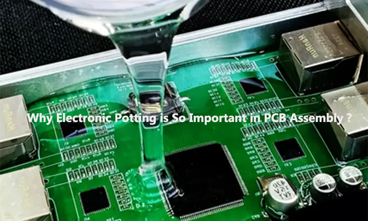
Electronic potting, also known as encapsulation or potting, is a process used to protect electronic components from environmental stress such as moisture, vibration, and shock. The process involves placing the electronic components into a potting material, which is then cured to create a hard, protective barrier around the components.
Electronic potting is commonly used in various industries, including aerospace, automotive, marine, and medical, to protect electronic components from harsh operating conditions. The process helps to increase the durability and reliability of electronic devices, ensuring they perform optimally and have a longer lifespan.
In this article, we will explore the electronic potting process, the materials used, and the benefits it provides. We will also discuss the different types of electronic potting materials available and the factors to consider when selecting the right potting material for a specific application.
What is Electronic Potting ?
In the field of electronics, potting is a process that involves filling an entire electronic assembly with a solid or gelatinous compound to protect it against shock, vibration, and moisture. While the transition from mechanical to electronic solutions has reduced the wear and material fatigue associated with moving parts, solid-state technology still faces challenges that can impact its reliability.
One such challenge is the issue of moisture in electronics, which can lead to false alarms, faulty operation, micro-corrosion, and ultimately, component and system failure. Accelerated aging is another concern, resulting from air pockets, gaps, and exposure to corrosive agents. Although these issues can be addressed by using suitable enclosures to protect vulnerable components and systems, this can increase cost and add size and weight.
Potting offers an alternative solution to mechanical encapsulation. The process involves encapsulating electronic components in suitable enclosures and compounds, similar to stabilizing the root system of a plant by placing it in a pot and filling it with soil. This method provides protection against shock, vibration, moisture, and corrosive agents, ensuring that vulnerable electronic components remain unharmed.
How Does Electronics Potting Work ?
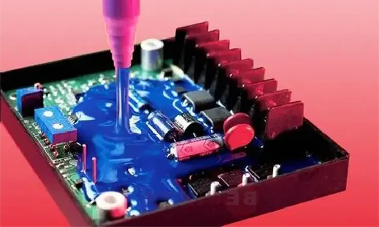
Electronic potting is a process that involves encapsulating electronic components in a specialized container, typically made of epoxies, polyurethanes, or silicones. These materials have thermal insulation and adhesive structural properties that protect the electronics from harsh environmental conditions and physical damage.
Potting can be achieved by creating a mold or cast that is removed once the potting compound has hardened, or by dipping components into the compound to encapsulate them. This process is highly flexible and can be applied to specific high-risk parts and components or to complete boards and assemblies.
The advantages of potting electronics are numerous. Potting materials are available in a variety of formulations that address conductivity, electrical and thermal isolation, and protection against various environmental conditions and threats. This flexibility allows designers and manufacturers to choose the best materials for their specific application needs.
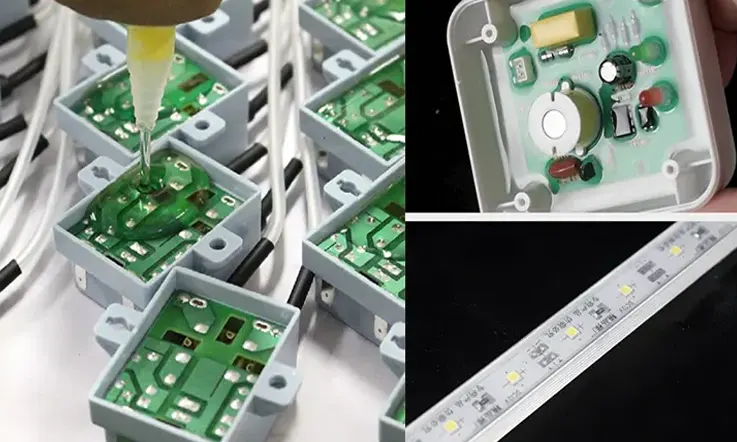
The Electronics Potting Process
The electronics potting process is a method of protecting electronic components and devices from environmental factors such as moisture, vibration, and shock. Potting involves encapsulating the electronic components in a protective material, typically a thermosetting polymer, to create a durable and long-lasting seal.
The process typically involves the following steps:
1. Preparation: The electronic components are cleaned, dried, and prepared for potting.
2. Mixing: The potting material is mixed according to the manufacturer’s instructions. This may involve combining two or more components, such as a resin and hardener.
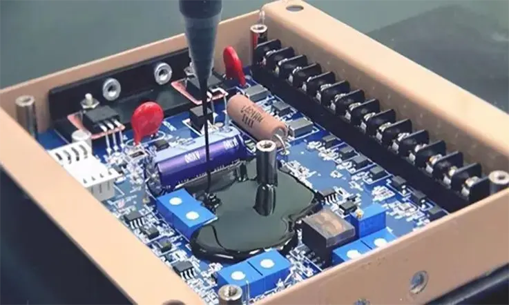
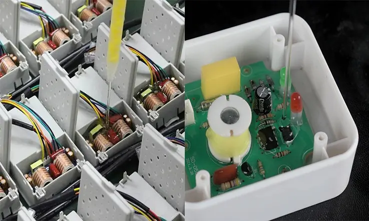
3. Potting: The mixed potting material is poured or injected into the enclosure or housing containing the electronic components. The potting material fills all the voids and covers the components completely.
4. Curing: The potting material is allowed to cure or harden, typically at room temperature or with the help of heat.
5. Finishing: After the potting material has cured, any excess material is trimmed or removed, and the electronic device is ready for use.
The potting material used can vary depending on the application and the desired properties. Common materials include epoxy resins, polyurethanes, and silicones. The material chosen should have good adhesion to the components and housing, provide a good seal, have good electrical properties, and be resistant to the expected environmental conditions.
The Benefits of Electronic Potting
Electronic potting is a highly effective method for protecting electronic devices and components, offering a range of benefits, including:
Environmental Protection: Potting materials act as a barrier against moisture, dust, dirt, and other environmental factors that can damage electronic components, ensuring optimal performance and longevity.
Durability Enhancement: Potting materials provide a protective layer around electronic components, making them more resistant to physical damage from vibration, impact, and shock, thereby increasing their durability.
Thermal Management Improvement: Many potting materials have excellent thermal conductivity properties, which can help to dissipate heat generated by electronic components, resulting in improved thermal management.
Increased Reliability: Potting helps to prevent corrosion and oxidation of electronic components, reducing the risk of failure and increasing device reliability.
Electrical Insulation Enhancement: Potting materials can enhance the electrical insulation properties of electronic components, reducing the risk of electrical shorts and other problems, thereby improving safety.
Customization Flexibility: Potting materials can be customized to meet specific design requirements, such as color, hardness, and flexibility, providing design flexibility to meet various application needs.
Overall, electronic potting is a valuable process for protecting electronic devices and components, and its benefits make it an essential consideration for many electronic design and manufacturing applications.
Electronic Potting Types
There are several methods of electronic potting, each with its own advantages and disadvantages. Here are some common electronic potting methods:
Manual potting: In this method, the potting material is poured or injected by hand into the enclosure or housing containing the electronic components. Manual potting is suitable for low-volume production runs or for prototyping, but it can be time-consuming and may not provide consistent coverage or quality.
Vacuum potting: In this method, the electronic components are placed in a vacuum chamber, and the potting material is injected under vacuum. This method helps to remove air bubbles and ensure complete coverage of the components, but it requires specialized equipment and can be expensive.
Pressure potting: In this method, the electronic components are placed in a pressure vessel, and the potting material is injected under pressure. Pressure potting helps to remove air bubbles and ensure complete coverage of the components, but it also requires specialized equipment and can be expensive.
Transfer potting: In this method, the potting material is poured into a potting tool or mold, and the electronic components are placed into the tool or mold. The potting material is then cured around the components. Transfer potting can provide consistent coverage and quality, but it requires specialized equipment and molds.
Injection molding: In this method, the potting material is injected into a mold containing the electronic components. The mold is then heated and cooled, and the cured potting material is removed from the mold. Injection molding can provide consistent coverage and quality, but it requires specialized equipment and molds.
In a words, the choice of electronic potting method depends on several factors, including the volume of production, the complexity of the electronic components, and the desired quality and consistency of the potting material.
How Does Potting Compare to Other Protective Solutions ?
Electronic potting is one of several protective solutions available for electronic components and devices. Here’s how it compares to other popular methods:
Conformal coating: Conformal coating involves applying a thin layer of protective material, such as epoxy or silicone, to the surface of a printed circuit board (PCB) or other electronic component. While conformal coatings can provide some protection against moisture and contaminants, they may not offer the same level of protection as potting, particularly against physical damage from vibration and shock.
Enclosures: Enclosures are physical structures that encase electronic components and devices, protecting them from environmental factors. While enclosures can provide a high level of protection, they may be bulky and may not be suitable for all applications.
Gasketing: Gasketing involves using a sealant or gasket to create a tight seal between electronic components and their housing. While gasketing can be effective in preventing moisture and dust from entering the enclosure, it may not offer the same level of protection as potting against vibration and shock.
All in all, while each protective solution has its own advantages and disadvantages, electronic potting is a highly effective method of protecting electronic components and devices from harsh environments and ensuring their long-term reliability.
What Are Materials Used in Electronic Potting and Encapsulation ?
JarnisTech Solutions provides a selection of materials suitable for electronic encapsulation and potting requirements, including epoxy, silicone, urethane, and acrylic coatings. Our range of coatings is tailored to meet the specific demands of your application, ensuring optimal protection and performance.
Epoxy coatings are a robust solution for harsh environments and physical security protection. We customize our epoxy coatings to meet your unique requirements, including high voltage or thermal concerns, ensuring that your assemblies are well-protected.
Silicone coatings are an excellent choice for superior protection against moisture exposure. Our silicone potting and encapsulation process uses a more forgiving material that guards assemblies against stress while allowing for movement.
Urethane coatings are also ideal for extreme environmental conditions, but their softer composition places less physical stress on protected assemblies.
Silicone potting and encapsulation process provides excellent resistance to environmental contaminants and direct pressure washing. This method also acts as a cushion or support system for LED components.
Acrylic coatings are a fast-drying solution that provides protection from moisture and environmental factors for printed circuit assemblies. At JarnisTech Solutions, we offer quality materials and customizable solutions to meet your electronic encapsulation and potting requirements.
How to Select the Best Compounds for Your Project ?
When selecting a potting compound for your application, there are several factors that you must consider. These factors include hardness, viscosity, color, and thermal conductivity. Each of these factors plays a crucial role in determining the suitability of a potting compound for a particular application.
Hardness is an essential factor when it comes to selecting a potting compound. Harder compounds are typically more resistant to weather and abrasion, making them ideal for applications that require robustness and durability. Epoxy and urethane are excellent selections for applications that require a hard and rigid compound, thanks to their hardness of up to 80D. On the other hand, silicon’s hardness ranges from 10A to 60A, making it a highly flexible yet hard enough option.
Viscosity is another critical factor to consider when selecting a potting compound. Most potting applications require low-viscosity compounds due to their flowability and self-leveling properties. Standard potting compounds are designed to meet these requirements. However, it is possible to request higher viscosity compounds if necessary.
Color is also an essential factor to consider, particularly if the color and visibility of the final product are critical. In such cases, it is essential to select the right potting compound color. However, a dark opaque color is sufficient for applications where color is not critical. It is worth noting that LEDs require transparent compounds for visibility.
Finally, thermal conductivity is a crucial factor to consider when selecting a potting compound. The ability to manage and dissipate heat generated by electronic devices is essential for their longevity and performance. Fortunately, silicone, epoxy, and urethane all offer excellent thermal conductivity, with silicone being the best option. Therefore, always opt for the potting compound with the highest thermal conductivity to ensure optimal heat management.
Factors to Consider When Choosing Electronic Potting Materials
When choosing electronic potting materials, there are several factors that need to be considered. These factors include:
Compatibility: The potting material must be compatible with the electronic components and the substrate. It should not react with the components or cause any damage to them.
Thermal Conductivity: Electronic components generate heat, and the potting material should have good thermal conductivity to dissipate the heat. This helps to prevent overheating and damage to the components.
Curing Time: The curing time of the potting material can be critical in certain applications. Some potting materials cure quickly, while others take longer. The curing time should be compatible with the production process and application requirements.
Chemical Resistance: The potting material should be resistant to chemicals that may come into contact with the electronic components. This is particularly important in harsh environments or applications where the potting material may be exposed to chemicals.
Mechanical Properties: The potting material should have suitable mechanical properties, such as flexibility, hardness, and strength. These properties are important in ensuring that the potting material can withstand the stresses and strains of the application.
Electrical Properties: The potting material should have good electrical insulation properties to protect the electronic components from electrical interference. It should also have suitable dielectric properties to prevent electrical breakdown.
Environmental Factors: The potting material should be able to withstand the environmental conditions of the application. This includes exposure to temperature extremes, humidity, and UV radiation.
Cost: The cost of the potting material is an important consideration in any application. The potting material should be cost-effective and provide good value for money, while still meeting the required performance criteria.
Why Choosing JarnisTech for Electronic Potting ?
20+ Years of Experience in Electronic Potting
JarnisTech is a trusted provider of electronic potting services with over 20 years of experience in the industry. Our extensive knowledge and expertise enable us to offer the best solutions to our customers.
Various Materials Available
We offer a wide range of materials for electronic potting, including epoxy, silicone, urethane, and acrylic. This diversity of materials ensures that we can handle diverse projects with ease. Our team of engineers and workers are proficient and professional, with in-depth knowledge of designing electronic potting solutions and operating them correctly.
The First-class Facility
We boast a first-class facility and continuously upgrade our potting machines to ensure high precision and homogeneous mixing of potting materials. Our industry-leading equipment helps increase production efficiency, enabling us to provide electronic potting services with short turnaround times.
High Efficiency
Efficiency is a core value at JarnisTech. Our experienced staff quickly understands the needs of customers, and our scientific internal processes and efficient communication with customers promote work progress and efficiency. We provide electronic potting services 24/7 to ensure that our customers receive the best service possible.
In summary, JarnisTech is a reliable and experienced provider of electronic potting services. Our diverse range of materials, expert team, state-of-the-art facility, and commitment to efficiency make us the ideal partner for any electronic potting project.
Applications of Electronic Potting
In today’s modern world, the widespread use of electronics has become commonplace in various industrial and daily life applications. However, electronic components are often exposed to harsh environmental conditions, including dirt, liquids, moisture, vibration, and extreme temperatures, which can lead to premature aging and failure. In this regard, potting has emerged as an essential technique to safeguard the optimal performance of electronic systems.
The automotive sector is a prime example of an industry that relies on numerous sophisticated electronic parts and systems. These components may be exposed to harsh environmental conditions, including moisture, heat, and vibration. By potting strategic parts and components, such systems can be protected from damage, premature aging, and failure, thus significantly enhancing their reliability.
Likewise, forklifts and other construction vehicles are frequently subjected to pressure washing at the end of their shifts, necessitating suitable electronic systems and conduits for reliable operation. In this context, potting can help protect critical components from the adverse effects of water and other environmental factors, ensuring their optimal performance and longevity.
In addition to the automotive and construction sectors, infrastructure electronics, including traffic lights, switches, power supplies, and sensors, are all critical components that depend on sealed enclosures for proper operation. However, aging, thermal and mechanical stress, UV exposure, and other factors can compromise the effectiveness of these enclosures, leading to a reduced lifespan and higher maintenance costs. Potting of strategic components can significantly increase the reliability of such systems, minimizing the need for costly repairs and replacements.
As a result, electronic potting is a crucial tool for ensuring the long-term reliability and performance of sensitive electronic systems exposed to harsh environmental conditions. Whether in automotive, construction, or infrastructure applications, potting can help protect vulnerable components from the detrimental effects of moisture, temperature, and other environmental factors, ultimately enhancing their lifespan and reducing maintenance costs.
Summary
In various applications, such as those involving printed circuit boards (PCBs) and electronic assemblies, protection against environmental factors such as dust, moisture, water, and other forms of physical damage is crucial. Electronic potting, which involves encapsulating the electronic components in a polymer resin, is a common method of achieving this protection. However, the effectiveness of the potting process is heavily dependent on the proper preparation and application of the potting compound.
Fortunately, a fundamental understanding of the potting process can help ensure successful outcomes. It is imperative to follow proper procedures for mixing and degassing the potting compound to prevent issues such as air bubbles and incomplete curing. The application process should also be carried out meticulously to ensure that the potting compound completely covers the electronic components and any potential gaps or voids are eliminated.
Overall, electronic potting is a critical process that demands attention to detail and adherence to proper protocols. By implementing the correct techniques, manufacturers can achieve optimal protection for their electronic assemblies and PCBs.
Related Posts:
- Mixed PCB Assembly Technology Services For Your Next New Project
- What Is Printed Circuit Boards Assembly?
- A Full Guide to Electro mechanical Assemblies
- Cable and Wire Harness Assembly
- Electronics Components PCB Assembly
- China:The Best PCB Consignment Assembly Services At JarnisTech
- PCB Box Build Assembly
- Nine Method of Save Cost PCB Assembly Production
- How Many Types of Turnkey PCB Assembly?