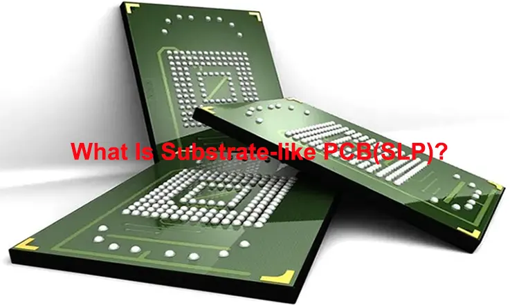
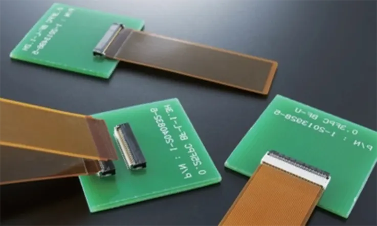
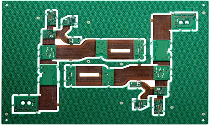
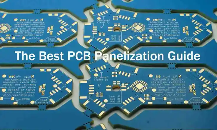
Substrate-like PCBs (SLPs) have emerged as a game-changing technology in the field of PCB design and manufacturing. With their unique characteristics and capabilities, SLPs are transforming the industry by enabling smaller chipsets, accommodating more components in limited space, and offering faster production cycles.
What Is SLP?
Substrate-like PCB (SLP) is essentially a high-end HDI board. From a manufacturing perspective, SLP is more similar to IC substrates used in semiconductor packaging, but it has not yet reached the level of IC substrates in terms of specifications. The core competitive advantage of SLP lies in the integration of board technology and HDI technology, which is reflected in the optimization capability of equipment and production lines, yield rate, and cost control. Its main difference from ordinary HDI lies in the minimum line width and spacing and the manufacturing process (mSAP – semi-additive process). SLP can be considered as an any-layer HDI board (interconnections on any layer) using the mSAP method.
Where Are Substrate-Like PCBs Used?
Substrate-like PCBs have emerged as a significant driving force in the PCB industry, primarily due to the rapid growth of the mobile device market. The continuous advancements in tablet, smartphone, and wearable technologies have necessitated more sophisticated device constructions and internal PCB designs. This trend has led to the development of smaller chipsets, allowing for the integration of an increasing number of features within a limited space. Furthermore, the demand for sleeker enclosures and larger batteries has compelled manufacturers to reduce the size of the PCBs.
A notable illustration of this trend can be observed in the recent implementations by industry giants Samsung and Apple. These companies have successfully incorporated substrate-like PCBs with linewidth/spacing dimensions of 25/25 μm and 30/30 μm in their devices. By employing these advanced PCBs, smartphones can now accommodate twice as many electronic components compared to traditional HDI boards within the same spatial constraints. This achievement is primarily attributed to the smaller linewidth of substrate-like PCBs. Additionally, the components utilized in these devices have become increasingly diminutive, with simpler components and chips now available in highly compact fine pitch BGAs packages.
Another noteworthy development is the integration of System-on-Chips (SoCs) within these devices. These SoCs are not only capable of performing multiple functions but also possess higher I/O density. Consequently, the need for numerous peripheral components that were traditionally present in such devices has been eliminated. It is worth mentioning that prominent Chinese smartphone manufacturers, including Oppo, Huawei, and Xiaomi, are expected to follow suit and adopt substrate-like PCBs in their product offerings.
The adoption of substrate-like PCBs in the mobile device market has revolutionized the PCB industry. The ability to accommodate more components in a smaller area, coupled with the integration of advanced chipsets, has paved the way for enhanced device capabilities and improved user experiences. As the market continues to evolve, we can anticipate further advancements and wider adoption of substrate-like PCB technology across various electronic devices.
SLP Manufacturing Technology
Currently, there are three main process technologies used in printed circuit board (PCB) and substrate manufacturing: subtractive process, additive process, and semi-additive process.
Subtractive Process:
The subtractive process is the earliest and most mature manufacturing technique for PCBs. It typically involves using photosensitive etching materials to transfer the circuit pattern and protect the areas that do not need to be etched. Then, an acid or alkaline etching solution is used to remove the unprotected copper layer.
Additive Process (SAP):
The additive process involves using an insulating substrate with photosensitive catalyst. After exposing the substrate to the circuit pattern, selective chemical copper deposition is used to create the conductor pattern.
Semi-Additive Process (MSAP):
The semi-additive process addresses the challenges of both subtractive and additive processes in creating fine circuit patterns. In this process, a chemical copper layer is formed on the substrate and a resist pattern is created on top. Through electroplating, the resist pattern is thickened and then removed. The excess chemical copper layer is removed using flash etching. The areas that were not thickened due to the resist protection are quickly removed during differential etching, leaving behind the desired circuit pattern.
Although SLP belongs to the category of printed circuit boards, its fine line width and spacing of 20μm/35μm cannot be produced using the subtractive process. Therefore, MSAP process technology is also required for SLP production.
SLP Tech vs. Standard PCB & IC Substrate: Differences
Substrate-like PCBs (SLPs) offer a fast and efficient solution for PCB fabricators to enable system designers to bring their systems to market quickly and with high yields. This is achieved through a carefully designed process that takes into account various critical factors, including component type, geometry, die-substrate mismatch, assembly steps, temperature ramp-up, cleaning, and electrical tests. These production details are often challenging for designers to anticipate and incorporate into their initial designs.
To illustrate this, consider the scenario where the power density (W/mm2) is excessively high, leading to the need for effective heat dissipation. In such cases, system engineers typically employ active dissipation devices to extract excessive heat from sensitive components. However, when collaborating with PCB design engineers to build an SLP, advanced heat dissipation techniques can be utilized. For instance, embedded coins with low coefficient of thermal expansion (CTE) can be incorporated into the SLP design. These coins efficiently pull heat from the components and direct it into a heat sink, reducing the reliance on additional active cooling systems such as fans, cooling fins, or cooling pipes. This not only saves costs but also conserves valuable space that would otherwise be occupied by these supplementary cooling devices. It is important to note that while heat dissipation is a critical step, it is not the sole focus of the SLP design process.
Therefore, traditional PCB designs rarely account for Chip-on-Board (CoB) and die cavity configurations. However, IC substrates, such as SLPs, are specifically designed to accommodate these specialized requirements, often deviating from the design considerations of regular surface mount device (SMD) components. By leveraging the advantages of SLP technology, PCB fabricators can streamline the design and manufacturing process, enabling system designers to introduce their systems to the market swiftly and with confidence in achieving high yields.
SLP Technology: High-Frequency/Speed Compatible?
Yes, SLP technology is well-suited for high-frequency or high-speed applications. The design and construction of substrate-like PCBs take into consideration various factors that are crucial for achieving optimal performance in these applications.
SLPs offer several advantages that make them suitable for high-frequency or high-speed applications. Firstly, the smaller dimensions and reduced parasitic effects of SLPs contribute to improved signal integrity and reduced signal loss, enabling higher-frequency operation. The smaller linewidth/spacing dimensions in SLPs allow for tighter trace routing and reduced crosstalk, which is particularly important in high-speed designs.
Additionally, SLPs provide enhanced thermal management capabilities, which are critical for high-frequency or high-speed applications that generate significant heat. The use of advanced heat dissipation techniques, such as embedded coins with low CTE, helps efficiently dissipate heat from components, preventing thermal issues that can degrade performance.
Furthermore, SLPs can be designed to accommodate specific requirements for impedance control, signal integrity, and transmission line characteristics. This ensures that high-frequency signals propagate effectively and minimize signal degradation.
It’s worth noting that the suitability of SLP technology for high-frequency or high-speed applications also depends on other factors such as the specific design requirements, materials used, and manufacturing processes employed. However, overall, SLPs offer a viable and efficient solution for achieving optimal performance in such applications.
Substrate-like PCB(SLP): System Reliability Impact?
When designing a system, it is crucial to carefully consider the Coefficient of Thermal Expansion (CTE) mismatch between the PCB, IC substrate, and die. The CTE mismatch can lead to reliability issues and performance degradation. However, Substrate-like PCBs (SLPs) provide a solution that effectively bridges the CTE gap between the PCB and IC substrate, resulting in significant benefits such as cost reduction and shorter production times.
By utilizing SLP technology, the CTE mismatch is minimized, ensuring better thermal stability and reliability of the system. SLPs are specifically engineered to have a CTE that closely matches that of the IC substrate and die. This compatibility reduces the stress and strain caused by temperature variations during operation, mitigating the risk of solder joint failures and other reliability concerns.
The ability of SLPs to bridge the CTE gap brings about notable advantages. Firstly, it lowers costs by reducing the need for additional measures to address the CTE mismatch, such as specialized materials or complex assembly processes. The compatibility between the PCB and IC substrate simplifies the manufacturing process and eliminates potential sources of failure, resulting in cost savings.
Secondly, SLPs contribute to shorter production times. The elimination of complex CTE compensation techniques streamlines the manufacturing process and allows for faster production cycles. This accelerated timeline enables system designers to bring their products to market more quickly, gaining a competitive edge.
All in all, SLPs offer a solution that effectively addresses the CTE mismatch between the PCB, IC substrate, and die. By bridging this gap, SLPs enhance thermal stability, reduce costs associated with CTE compensation, and expedite production times. System designers can benefit from the improved reliability and efficiency provided by SLP technology, enabling them to deliver high-quality products in a timely and cost-effective manner.
How SLP Technology Overcoming High Power Overheating?
Thermal management is an increasingly critical concern in both bare PCB and assembly levels, particularly in high-power and high-voltage applications. To address the need for improved heat transfer and cooling solutions, the adoption of copper coin inserts, often made of Copper Molybdenum Copper (CMC), has become common.
The copper coin heat dissipation method involves the integration of a solid copper piece onto or into the PCB, typically positioned beneath specific component(s) that require effective cooling. Compared to a via farm, the copper coin offers approximately ten times better cooling performance. By establishing direct contact between the heat-generating component pad and the heat sink, the copper coin facilitates efficient heat transfer without relying on thermally conductive materials.
Copper coin technology is particularly suitable for scenarios where one or a few components on the PCB generate significant heat. It provides an optimal heat transfer solution in a localized manner, regardless of the number of PCB layers or the chosen PCB material. Moreover, the adoption of copper coins significantly reduces the weight of the substrate when compared to traditional heat sinks or active cooling elements.
Summary
Substrate-like PCBs (SLPs) have revolutionized the PCB industry by bridging the gap between traditional PCB designs and IC substrates. By minimizing the Coefficient of Thermal Expansion (CTE) mismatch, SLPs ensure better thermal stability and reliability of systems, while reducing costs and production time. The integration of copper coin inserts further enhances thermal management, making SLPs ideal for high-power and high-voltage applications.
As Chinese manufacturers follow the footsteps of industry leaders like Samsung and Apple, the adoption of SLP technology is expected to increase. With improved signal integrity, reduced signal loss, and enhanced thermal management, SLPs pave the way for more efficient and compact electronic systems. The era of Substrate-like PCBs has arrived, promising a future of advanced PCB designs and accelerated innovation.
Advancements in technology have led to significant progress in the PCB (Printed Circuit Board) industry, driven by the growing demands within the electronics sector. PCBs play a pivotal role in the efficient functioning of electronic devices, making them an essential component in electronics production.
Notably, researchers have embarked on experimental endeavors to explore the potential of 3D printing in PCB manufacturing, and the outcomes have been highly promising. The utilization of 3D printed PCBs has become increasingly prevalent across the electronics industry. This article aims to delve into the domain of 3D printed PCBs, analyzing their significance and impact.
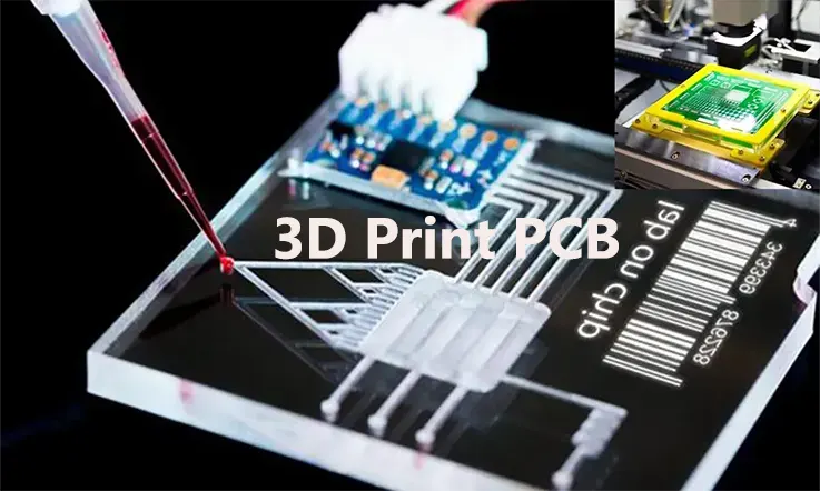
What is a 3D Print PCB?
When referring to a 3D PCB, it should be noted that it does not imply a three-dimensional circuit board. Rather, a 3D PCB is a type of circuit board manufactured using a 3D printer. In this process, the board’s circuits are printed directly onto the bare board using a 3D inkjet printer, eliminating the need for traditional copper etching techniques.
A 3D PCB employs a 3D inkjet printer equipped with an extruder head, which utilizes specialized gel or conductive materials. This printer is capable of accurately printing circuits onto a bare PCB board. The utilization of 3D printing technology in PCB manufacturing offers several advantages over conventional methods, including reduced errors and minimized waste material. The adoption of 3D PCBs has had a significant impact on the electronics manufacturing industry.
It is worth noting that 3D printing can produce both single-sided and double-sided PCBs with relative ease. Furthermore, applying a 3D printer to a flexible PCB is a straightforward process. However, printing a multilayer board presents a more complex challenge, which can be facilitated through the utilization of PCB design software.
Methods of 3D Printing PCBs
3D printing of printed circuit boards (PCBs) is a relatively new technology that allows for the quick prototyping and production of complex electronic devices. The major methods of 3D printing PCBs are as follows:
Fused Deposition Modelling (FDM)
FDM is the most common method of 3D printing. It works by heating and extruding a thermoplastic filament layer by layer onto a build plate. In the case of PCBs, a conductive filament can be used to create the circuit pathways.
Though FDM is not typically used for creating commercial-grade PCBs due to its relatively low resolution, it can be useful for prototyping simple circuits and for educational purposes.
Inkjet Printing
Inkjet printing involves depositing droplets of conductive ink onto a substrate. The ink is typically composed of silver or other conductive metals. The droplets of ink are deposited in the shape of the desired circuit pattern, and once the ink is dried or cured, a conductive pathway is formed.
Inkjet printing allows for the creation of complex, high-resolution circuits, making it suitable for commercial applications. However, the inks used can be expensive, and the process requires precise control over the deposition of the ink.
Aerosol Jet Printing
Aerosol jet printing is similar to inkjet printing, but instead of depositing droplets of ink, it sprays a fine mist of conductive ink onto the substrate. This allows for the creation of very fine, high-resolution circuit pathways.
Aerosol jet printing can be used to create complex, 3D circuits on a variety of substrates, making it a versatile method for 3D printing PCBs.
Selective Laser Sintering (SLS)
SLS involves using a high-power laser to fuse small particles of plastic, metal, ceramic, or glass powders into a mass that has the desired 3-dimensional shape. SLS can be used to create PCBs by using a conductive powder to form the circuit pathways.
SLS allows for the creation of complex, high-resolution circuits, and it can be used with a variety of materials. However, it requires a high-power laser and precise control over the sintering process.
Direct Laser Writing (DLW)
DLW is a method that uses a focused laser beam to pattern a photosensitive material. The laser beam alters the properties of the material, creating conductive pathways. This method can be used to create high-resolution, complex circuits.
DLW is a relatively slow process, but it allows for a high degree of control over the circuit design, making it suitable for creating complex, high-performance circuits.
It’s important to note that while 3D printed PCBs have many advantages, such as rapid prototyping and the ability to create complex circuits, they currently do not match the performance and reliability of traditional PCBs. However, as 3D printing technology continues to advance, the gap is likely to narrow.
Benefits and Challenges of PCB 3D Printing
3D printing technology has significantly transformed many industries, and the electronics sector is no exception. Printed circuit board (PCB) 3D printing is one of the emerging technologies that has the potential to revolutionize the way we design and manufacture electronic devices. This technology involves the use of additive manufacturing to create a PCB layer by layer.
Let’s look at both the benefits and challenges of 3D-printed PCBs:
Benefits
Rapid Prototyping: One of the most significant advantages of PCB 3D printing is the ability to quickly create prototypes. Designers can print a circuit board, test it, modify the design, and reprint it in a short period, accelerating the development process.
Complex Designs: Traditional manufacturing methods can limit the complexity of the PCBs. 3D printing allows for more intricate designs, including multi-layer PCBs with integrated components.
Cost-Effective for Small Runs: Traditional PCB manufacturing involves high setup costs, making it expensive for small production runs. However, 3D printing can be cost-effective for producing small quantities.
Reduced Waste: 3D printing is an additive process, where material is added layer by layer, which can reduce waste compared to traditional subtractive manufacturing methods.
Customization: 3D printing allows for high levels of customization without significantly increasing costs. This can be beneficial for making customized electronics or devices for specific applications.
Challenges
Limited Materials: Currently, there are limitations on the types of materials that can be used for 3D printing PCBs. Typical 3D printers use thermoplastics, which may not have the necessary electrical properties for some applications.
Resolution and Precision: While 3D printing technology continues to improve, traditional manufacturing methods can often provide higher resolution and precision. This can be a significant challenge for PCBs, which often require precise, miniaturized components.
Speed: 3D printing is generally slower than traditional manufacturing methods, especially for large quantities. This makes it less suitable for mass production.
Durability and Quality: While 3D printed PCBs are suitable for prototyping, there may be concerns about their durability and quality for long-term use or in harsh environments.
Regulatory Challenges: As with any new technology, there can be regulatory challenges. Standards and regulations for 3D printed electronics are still in development, which could slow adoption.
In conclusion, while PCB 3D printing offers many advantages like rapid prototyping, complex designs, and cost-effectiveness for small runs, it also faces challenges such as limited materials, lower precision, slower speed, and concerns about durability and quality. Despite these challenges, as the technology continues to evolve, it is likely to become an increasingly important tool in electronics design and manufacturing.
Applications of 3D Printed Circuit Boards
3D printed circuit boards (PCBs) offer several unique advantages and applications compared to traditional PCB manufacturing methods. Here are some of the applications of 3D printed circuit boards:
Rapid Prototyping: 3D printed PCBs allow for rapid prototyping of electronic circuits. Design iterations can be quickly implemented and tested, reducing the time and cost involved in developing new electronic devices.
Custom Electronics: 3D printing enables the creation of custom-shaped PCBs that can fit into unconventional or compact spaces. This is particularly useful in devices with complex geometries or wearable electronics where space is limited.
Embedding Components: With 3D printed PCBs, components can be directly integrated into the printed structure, eliminating the need for additional assembly steps. This enables the creation of highly integrated devices with reduced size and weight.
Lightweight Electronics: By utilizing additive manufacturing techniques, 3D printed PCBs can be designed with lightweight structures, which is beneficial in applications such as drones, satellites, and aerospace systems, where weight reduction is critical.
Antenna Integration: 3D printed PCBs can incorporate antennas directly into the structure. This allows for the creation of compact and customized antennas that are well-suited for wireless communication devices.
Low-Volume Production: For low-volume production runs, 3D printing can be a cost-effective alternative to traditional PCB manufacturing methods. It eliminates the need for expensive tooling and setup, making it suitable for small-scale production or customized electronic devices.
Education and Research: 3D printed PCBs are valuable tools for educational institutions and research laboratories. They provide a hands-on learning experience for students, allowing them to design and fabricate functional circuits more easily.
IoT Devices:Internet of Things (IoT) devices often require compact and customized electronics. 3D printed PCBs can be used to create IoT devices with integrated sensors, microcontrollers, and wireless communication modules.
Flexible Electronics: Some 3D printing technologies allow for the creation of flexible PCBs. This flexibility is advantageous in applications where the circuit needs to conform to curved surfaces or undergo bending and stretching, such as wearable electronics or medical devices.
Repair and Replacement: 3D printed PCBs can be used to create replacement parts for legacy systems or obsolete components. This can extend the operational lifespan of older equipment that is no longer supported by traditional manufacturing methods.
It’s worth noting that while 3D printed PCBs offer several advantages, they also have limitations. The level of complexity and density achievable with 3D printed PCBs may be lower compared to traditional manufacturing methods. Additionally, the electrical and thermal properties of the printed materials may differ from those of conventional PCB materials, which can impact performance and reliability.
How to Choose the Optimal 3D Printing Process for PCBs?
Selecting the appropriate 3D printing process for your PCBs requires careful consideration of various factors. To make an informed decision, follow these steps:
1. Understand your requirements: Begin by clearly defining your project’s specific requirements. Consider factors such as the complexity of the circuit design, desired conductivity, mechanical strength, weight limitations, cost constraints, and any other relevant specifications.
2. Research available processes: Thoroughly investigate the 3D printing processes commonly used for PCB manufacturing, such as Fused Deposition Modeling (FDM), Multi Jet Fusion (MJF), or lamination methods. Understand the principles behind each process, their strengths, limitations, and the materials they are compatible with.
3. Evaluate material properties: Assess the conductivity, thermal and electrical properties, and mechanical strength of the materials compatible with each printing process. Compare these properties against your project requirements to ensure they align with the intended application of the PCB.
4. Consider design complexity: Determine the complexity of your circuit design. Some 3D printing processes may be better suited for intricate and densely packed designs, while others may struggle with fine details or multiple layers. Evaluate the capabilities of each process in relation to your design complexity.
5. Review cost considerations: Examine the cost implications associated with each 3D printing process. Evaluate not only the initial investment required for the printer but also the recurring expenses for materials, maintenance, and post-processing. Consider the long-term cost-effectiveness of each process for your specific production volumes.
6. Seek expert advice: Consult with experts or professionals experienced in 3D printing and PCB manufacturing. They can provide valuable insights and recommendations based on their knowledge and expertise, helping you make an informed decision.
7. Test and iterate: Before committing to mass production, consider prototyping and testing your PCB designs using different 3D printing processes. This hands-on experimentation will allow you to evaluate the quality, performance, and compatibility of each process with your specific requirements.
By carefully considering these steps and thoroughly researching the available options, you can confidently choose the most suitable 3D printing process for your PCB manufacturing needs. Remember to prioritize the alignment of material properties, design complexity, cost considerations, and expert advice to ensure successful outcomes.
What Are The Different Between PCB Manufacturing and 3D Printing PCB?
PCB manufacturing and 3D printing PCB are two distinct approaches to producing printed circuit boards, each with its own characteristics and processes. Here are the key differences between them:
Manufacturing Techniques
PCB Manufacturing: Traditional PCB manufacturing involves a subtractive process. It starts with a copper-clad substrate, and various steps such as etching, drilling, and plating are employed to create the desired circuit pattern.
3D Printing PCB: 3D printing, also known as additive manufacturing, builds PCBs layer by layer. It uses specialized 3D printers that deposit materials, such as conductive inks or resins, to create the circuitry and components in a three-dimensional manner.
Design Flexibility
PCB Manufacturing: Traditional manufacturing techniques offer a high level of design flexibility. Complex circuitry, multiple layers, and various components can be easily accommodated.
3D Printing PCB: 3D printing enables unique design possibilities, such as embedding components within the PCB, creating unconventional shapes, and integrating intricate geometries. This allows for greater design freedom but may have limitations in terms of electrical performance and material selection.
Prototyping and Customization
PCB Manufacturing: Traditional PCB manufacturing is well-suited for mass production but can be time-consuming and costly for prototyping or small-scale customization.
3D Printing PCB: 3D printing excels in rapid prototyping and low-volume customization. It enables quicker design iterations, reduces setup costs, and facilitates on-demand production of customized PCBs.
Material Selection
PCB Manufacturing: Traditional PCB manufacturing primarily uses rigid materials, such as FR-4, which offer good electrical performance and durability.
3D Printing PCB: 3D printing allows for a wider range of material options, including conductive inks, flexible substrates, and even composite materials. However, the electrical properties and mechanical strength of these materials may vary compared to those used in traditional PCBs.
Production Scale
PCB Manufacturing: Traditional PCB manufacturing processes are highly scalable, making them suitable for large-scale production.
3D Printing PCB: 3D printing is more commonly used for smaller-scale production, prototyping, and customized applications. Scaling up 3D printing for mass production can be challenging due to limitations in speed and material compatibility.
It’s important to note that both approaches have their strengths and are often used in conjunction with each other. PCB manufacturing is well-established and widely adopted, offering reliability and efficiency for large-scale production. 3D printing PCB, on the other hand, is favored for its design flexibility, rapid prototyping capabilities, and customization options.
Future of 3D Printed Circuit Boards
The future of 3D printed circuit boards (PCBs) holds immense potential for the electronics manufacturing industry. Here are some key aspects that shape the future of 3D printed PCBs:
Advancements in Materials: Ongoing research and development efforts are focused on expanding the range of materials suitable for 3D printing PCBs. This includes the development of conductive inks, flexible substrates, and multi-functional materials that offer enhanced electrical and mechanical properties. The availability of a wider selection of materials will enable the production of more diverse and complex PCB designs.
Improved Printing Technologies: 3D printing technologies continue to evolve, becoming more precise, efficient, and capable of producing intricate PCB structures. Advancements in printing techniques, such as higher resolution and finer nozzle sizes, will enable the creation of smaller components and finer circuit traces. Enhanced printing technologies will facilitate the production of complex multilayer boards with improved reliability and performance.
Integration of Electronics and Structures: 3D printing allows for the seamless integration of electronic components within the physical structure of a product. This opens up new possibilities for embedding sensors, antennas, and other circuitry directly into objects, enabling the creation of smart and connected devices. This integration of electronics and structures can lead to innovative applications in fields like healthcare, automotive, aerospace, and IoT.
Design Freedom and Customization: 3D printing offers unparalleled design freedom, enabling the creation of highly customized PCBs tailored to specific applications. Designers can optimize the circuit layout, shape, and orientation to maximize performance and functionality. This customization potential allows for rapid prototyping, iterative design improvements, and the production of small-batch or on-demand PCBs, reducing time-to-market and overall costs.
Sustainability and Waste Reduction: 3D printing can contribute to sustainable manufacturing practices by minimizing material waste compared to traditional subtractive manufacturing methods. With precise material deposition, only the required amount of material is used, reducing scrap. Additionally, advancements in recyclable and eco-friendly materials for 3D printing contribute to a more sustainable PCB manufacturing process.
Integration with AI and Automation: The integration of 3D printing with artificial intelligence (AI) and automation technologies holds promise for streamlining the PCB manufacturing process. AI algorithms can optimize designs for additive manufacturing, enhance quality control, and automate post-processing tasks. This integration will lead to increased efficiency, productivity, and scalability in 3D printed PCB production.
Overall, the future of 3D printed PCBs is poised for significant advancements in materials, printing technologies, design capabilities, sustainability, and automation. These developments will revolutionize the electronics manufacturing landscape, enabling the production of highly customized, efficient, and integrated PCBs for a wide range of applications.
Summary
The advent of 3D printed circuit boards is revolutionizing the landscape of electronics design and production. By harnessing the capabilities of 3D printing technology, developers now have the ability to fabricate circuit boards in virtually any desired shape. This newfound flexibility fosters a heightened level of creativity and innovation within the electronics industry.
To explore further details about the potential of 3D printed circuit boards, we invite you to get in touch with Circuits Central. Our knowledgeable team is available to provide comprehensive information and address any inquiries you may have. Please feel free to reach out to us at 0086-0755-23034656 or by contacting us through our website. We look forward to assisting you in unlocking the possibilities offered by 3D printed circuit boards.
Welcome to our comprehensive guide, where we provide valuable insights into selecting the ideal material for your PCB. As a leading PCB manufacturer, we understand the importance of choosing the right PCB laminate material. In this guide, we will meticulously explore the diverse range of PCB laminate materials currently available in the market.
Whether you are a seasoned engineer or a beginner, we invite you to delve into the world of PCB laminates and expand your knowledge in this crucial aspect of PCB fabrication.
What is Laminate in PCB?
In the context of PCB (Printed Circuit Board) manufacturing, a laminate refers to the base material used to construct the PCB. It is a composite material composed of multiple layers, typically consisting of a substrate and a copper foil layer. The laminate serves as the foundation for the PCB, providing mechanical support and electrical insulation between the different circuit layers.
The substrate material in the laminate, often made of fiberglass-reinforced epoxy resin (FR-4), provides structural integrity and stability to the PCB. It is a non-conductive material that acts as an insulator, preventing electrical shorts between the copper layers.
The copper foil layer, bonded to the substrate, forms the conductive pathways and traces on the PCB. It allows for the flow of electrical signals throughout the board, connecting various components and circuitry.
Laminates can vary in thickness, dielectric constant, and other properties, depending on the specific requirements of the PCB design and its intended application. Different types of laminates offer distinct characteristics, such as high-frequency performance, thermal conductivity, or flexibility, catering to a wide range of PCB design needs.
Overall, the laminate is a critical component in PCB fabrication, providing the necessary structural integrity, electrical insulation, and conductive pathways required for the proper functioning of the circuit board.
PCB Laminate Materials for PCB Manufacturing
PCB (Printed Circuit Board) laminate materials are essential in the manufacturing of PCBs. They provide the mechanical base and electrical interconnection for the components of the electronic devices. The choice of laminate material affects the performance, reliability, and cost of the final product. Here are some of the most common PCB laminate materials:
FR-4
This is the most widely used material in PCB manufacturing. FR-4 is a composite material composed of woven fiberglass cloth with an epoxy resin binder. The “FR” stands for “flame retardant”. It offers a good balance of electrical properties, mechanical strength, cost, and performance.
High-Temperature Laminates (e.g., Polyimide)
These materials are used for applications requiring high operating temperatures, such as in aerospace and automotive industries. Polyimide laminates are known for their thermal stability, good chemical resistance, and excellent mechanical properties.
PTFE (Teflon)
This is used for high-frequency applications due to its low dielectric constant and low signal loss characteristics. However, it’s more difficult to work with and is more expensive than FR-4.
CEM (Composite Epoxy Material)
CEM materials are similar to FR-4 but have a mixture of woven glass and non-woven glass fibers. Common types include CEM-1 and CEM-3. They are less expensive and have slightly different electrical properties.
BT-Epoxy
BT-Epoxy is a thermoplastic that has lower moisture absorption and better heat resistance than FR-4. It’s often used for IC substrates.
Aluminum (Metal Core PCBs)
Aluminum-backed PCBs are used for high power applications and LED lights where heat dissipation is a concern. The aluminum is used as a heat sink to help dissipate heat away from the circuit.
Rogers Material
A brand of high-frequency laminate materials. They are used when FR-4’s electrical, thermal, or mechanical performances aren’t sufficient.
When choosing a laminate material, factors such as operating temperature, required electrical properties (like dielectric constant and loss tangent), mechanical strength, cost, and the specific requirements of the final application should be considered. The choice of laminate can significantly influence the performance and reliability of the final product.
Considerations Selecting Printed Circuit Board laminates Material
When it comes to selecting the right laminate material for printed circuit boards (PCBs), there are several important considerations to keep in mind. These considerations include:
Electrical Performance: Evaluate the electrical properties of the laminate, such as dielectric constant, loss tangent, and impedance control. The chosen material should provide the required electrical performance for your circuit design.
Thermal Management: Consider the thermal properties of the laminate, including thermal conductivity and coefficient of thermal expansion (CTE). These properties are crucial for effective heat dissipation and preventing thermal stress on components.
Mechanical Strength: Assess the mechanical strength and rigidity of the laminate material. It should be able to withstand the mechanical stresses encountered during PCB fabrication, assembly, and operation.
Dimensional Stability: Look for laminates with low moisture absorption and CTE to ensure dimensional stability over a wide range of environmental conditions. This helps prevent warping or distortion of the PCB.
Chemical Resistance: Consider the laminate’s resistance to chemicals, solvents, and other substances it may come into contact with during its lifespan. This is particularly important in harsh or corrosive environments.
Fabrication Compatibility: Ensure that the chosen laminate material is compatible with the manufacturing processes involved in PCB fabrication, such as etching, drilling, and soldering.
Cost-Effectiveness: Evaluate the cost of the laminate material and ensure it aligns with your budget while meeting the required performance criteria.
Industry Standards and Certifications: Verify that the laminate material complies with industry standards and certifications. This ensures reliability, safety, and regulatory compliance for your PCB.
Application-Specific Requirements: Consider any specific requirements of your application, such as high-frequency performance, impedance control, or specialized environmental conditions. Choose a laminate material that can meet these unique needs.
By carefully considering these factors, you can select a PCB laminate material that meets the electrical, thermal, mechanical, and environmental requirements of your specific application. This ensures optimal performance, reliability, and longevity of your printed circuit boards.
Difference Between Laminates and Prepregs
Laminates and prepregs are two distinct components used in the construction of printed circuit boards (PCBs). Although they are related, there are differences between the two:
Laminates: Laminates are composite materials consisting of multiple layers. They typically comprise a core substrate material, such as fiberglass-reinforced epoxy resin (FR-4), with a copper foil bonded to one or both sides. Laminates provide the structural foundation of the PCB and contribute to its mechanical strength and rigidity. They are available in various thicknesses and offer different electrical and thermal properties.
Prepregs: Prepregs, short for pre-impregnated materials, are also composite materials used in PCB manufacturing. Prepregs consist of a reinforcement material, such as fiberglass, impregnated with a resin, typically epoxy. Unlike laminates, prepregs do not have a copper foil layer bonded to them. Instead, they are used to build up the internal layers of a multilayer PCB. Prepregs are placed between copper layers or cores and are then subjected to heat and pressure during the lamination process. The heat causes the resin to flow and bond the layers together, creating a solid PCB structure.
In summary, laminates form the base material of the PCB, providing mechanical support and electrical insulation, while prepregs are used to create the internal layers of multilayer PCBs, serving as the adhesive material that bonds the layers together during the lamination process. Both laminates and prepregs are essential components in PCB fabrication, with each playing a specific role in the construction of the final PCB structure.
Importance of laminates in PCB fabrication
The utilization of laminates in PCB manufacturing is driven by several crucial factors that contribute to the overall success of the fabrication process. These key traits include enhanced impedance control, low moisture absorption, improved thermal management, and consistent performance in dynamic thermal reactions. As the electronic industry continues to evolve through discoveries and innovations, high-frequency laminates have emerged as a fundamental element for the advancement of PCB technologies.
JarnisTech excels in providing professional PCB layout and fabrication services, leveraging our skilled team of researchers and technical experts. We have developed effective lamination solutions tailored to your specific PCB projects. Our expertise encompasses a wide range of capabilities, including high-frequency laminates, achieving tighter hole-to-hole pitch, implementing exotic via structures, accommodating multiple lamination cycles, ensuring lead-free or halogen-free solder assembly with strict environmental considerations, and supporting high operating temperatures. These highlights demonstrate our commitment to incorporating robust laminate technologies.
To address any inquiries or request a quote, please feel free to reach out to us via email at [email protected] or by phone at 0086-0755-23034656. We are dedicated to providing solutions and assisting you in achieving your PCB objectives.
Benefits of Choosing a Reliable PCB Laminate Manufacturer
The selection of a dependable PCB laminate manufacturer holds paramount importance in guaranteeing the quality, reliability, and performance of your electronic devices. Here are several benefits associated with choosing a reliable PCB laminate manufacturer:
High-Quality Materials: A reliable manufacturer utilizes top-notch materials that ensure the durability and reliability of your PCBs. These materials exhibit resistance to heat, moisture, and other environmental factors that could potentially impact the performance of your electronic devices. By employing high-quality materials, manufacturers extend the lifespan of your PCBs, minimizing the need for frequent repairs or replacements.
Consistent Quality: A reputable PCB laminate manufacturer adheres to stringent quality control processes, ensuring that every PCB meets required standards. Utilizing advanced testing equipment, they meticulously identify and rectify any defects or issues in the PCBs, enabling consistent quality. Such consistency significantly reduces the risk of failures or malfunctions in your electronic devices.
Customization Options: A reliable manufacturer offers customized solutions tailored to your specific requirements. With their expertise and knowledge, they can design and manufacture PCBs that precisely align with your needs, optimizing the performance of your electronic devices. Customization options encompass various aspects such as size, shape, materials, and the integration of specific features or functionalities.
Cost-Effectiveness: Opting for a reliable PCB laminate manufacturer can yield long-term cost savings. By utilizing high-quality materials and implementing stringent quality control measures, they mitigate the risk of failures or malfunctions in your electronic devices. This, in turn, reduces the frequency of repairs or replacements, translating into significant cost savings over time.
Timely Delivery: Recognizing the significance of timely delivery, a dependable PCB laminate manufacturer maintains a streamlined manufacturing process. This ensures that your PCBs are delivered punctually, minimizing any disruptions in your production timeline. Timely delivery allows you to meet your deadlines, ensuring that your electronic devices are available to your customers as planned.
All in all, the meticulous selection of a reliable PCB laminate manufacturer is essential for upholding the quality, reliability, and performance of your electronic devices. Their provision of high-quality materials, consistent quality, customization options, cost-effectiveness, and adherence to timely delivery schedules makes them an ideal choice for your PCB manufacturing needs.
Summary
With an extensive industry experience spanning over two decades, JarnisTech proudly stands as a leading PCB and PCB assembly manufacturer based in China. Our expertise lies not only in providing quick-turn PCB prototypes and assembly services but also in catering to medium and small volume PCB fabrication requirements. We possess a specialized focus on lamination and sequential lamination techniques, ensuring the long-term cost-effectiveness and optimal functionality of electronic devices.
Circuit board laminates serve multiple purposes in PCB construction, including providing electrical insulation between copper traces, offering mechanical support for electronic components, and ensuring consistent dielectric properties for optimal transmission of electrical currents through the copper traces without attenuation.
When working with circuit board laminates, it is advisable to seek guidance from a professional PCB manufacturer-JarnisTech. Our expertise can help ensure the appropriate selection and use of these materials in your circuit boards, leading to reliable and high-performance PCB assemblies.
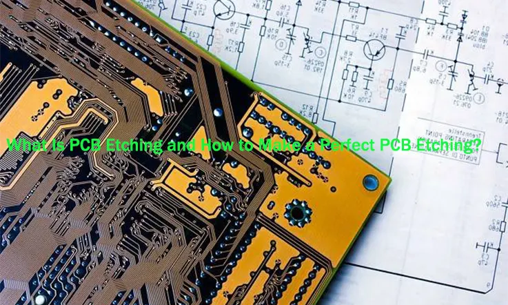
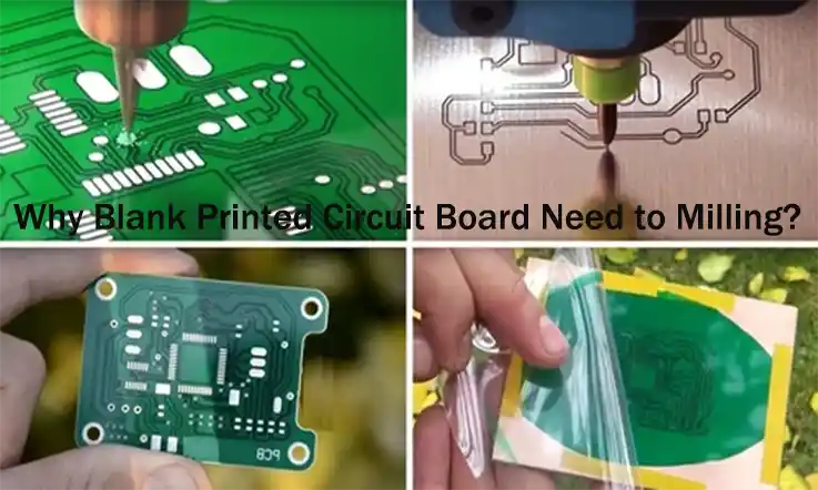
Printed Circuit Boards (PCBs) are the backbone of most electronic devices. They provide a physical base for mounting and interconnecting components, and they play a crucial role in the operation of electronics. The process to manufacture a PCB involves various steps, one of the most vital of which is the etching process.
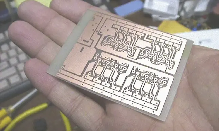
Printed circuit boards (PCBs) play a pivotal role in the electronics industry, offering both widespread usage and cost-effectiveness. They enable the assembly of intricate circuits within confined spaces, effectively minimizing the risk of loose connections. In industrial settings involved in PCB manufacturing, various methods and specialized machinery are employed. However, it is also possible to carry out PCB etching at home with relative ease. This article provides valuable insights into the realm of DIY PCB etching and factory PCB etching, encompassing essential steps, required tools, and safety precautions, among other pertinent aspects.
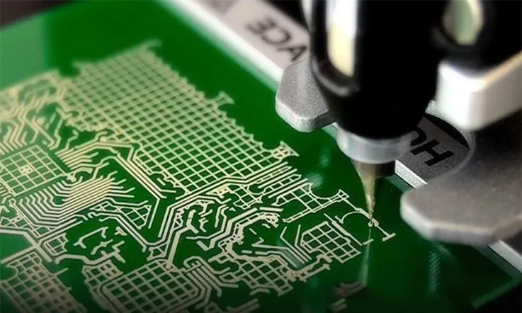
What is PCB Etching?
PCB etching is the process of removing unwanted copper from the board to create a planned circuit layout. This process is integral to circuit board manufacturing as it shapes the pathways for electricity to travel throughout the board.
Furthermore, the etching process employed by industrial circuit board fabricators can be divided into two distinct methods: acidic etching and alkaline etching.
Acidic Etching
Acidic etching is specifically employed in the elimination of copper from internal layers in standard rigid FR-4 circuit boards. This choice is attributed to its capacity for precise and less aggressive action. The acidic process exhibits compatibility with the photoresist material and results in minimal undercutting during the metal etching process. Nonetheless, it is important to acknowledge that acidic etching entails a longer duration compared to alternative methods, thus necessitating a trade-off in terms of time efficiency.
Alkaline Etching
Alkaline etching is employed for the outer layers of circuit boards, as it offers a faster process that helps maintain the uniformity of the remaining copper. Alkaline etching, being more active than acidic etching, necessitates meticulous monitoring to ensure precise execution.
The utilization of both acidic and alkaline etching processes is advantageous due to their high etching rates, cost-effectiveness, and ability to effectively etch various metal materials. PCB fabricators must diligently uphold their etching procedures to mitigate exposure to hazardous liquids and fumes, as well as prevent any potential water contamination. Now, let us delve into the application of this etching technique in the fabrication of printed circuit boards.
The Etching Process of PCB Factory
The etching process can be broken down into four main steps:
1. Laminating: The process begins with a substrate (usually fiberglass) covered with a thin layer of copper. This copper is laminated with a resist layer, which is a type of material that’s resistant to the etching solution. This layer is typically photoresist, which is sensitive to light.
2. Exposing: The board, covered in resist, is then exposed to ultraviolet light. A mask, also known as a stencil or photomask, is used to cover the areas of the board that should remain copper. The UV light hardens the exposed photoresist.
3. Developing: After exposure, the board is bathed in a developing solution. This solution removes the unhardened photoresist from the areas not exposed to the UV light, revealing the copper underneath.
4. Etching: The board is then submerged in an etchant solution, often ferric chloride or ammonium persulfate, which dissolves the exposed copper. The hardened photoresist protects the copper beneath from the etchant, and thus the desired circuit pattern is left on the board.
5.Stripping: Finally, the remaining photoresist is stripped away, leaving a clean, etched board ready for the next stages of PCB production.
Importance of PCB Etching
Etching is crucial as it shapes the pathways that allow electricity to flow between different components on the PCB. It ensures that the circuits are accurate and precise, which is vital for the reliable operation of the final electronic product.
Without the etching process, it would be impossible to create the complex, multi-layered circuit designs that are typical in modern electronics. It is a cost-effective method that enables mass production of high-quality, consistent PCBs.
DIY:Materials and Necessary Tools
The subsequent list encompasses key tools and materials that are essential for undertaking the process of DIY PCB etching.
♦ Ferric Chloride, also known as the Etching solution
Prior to delving into the step-by-step process of PCB etching at home, it is crucial to emphasize the indispensability of the aforementioned materials and equipment. Their availability is paramount to ensure the successful execution of the PCB etching procedure.
For instance, the absence of rubber gloves can lead to discomfort and potential harm to your hands. Similarly, the lack of steel wool or sandpaper will impede the effective removal of the top oxide layer from the copper material and hinder proper adhesion of the image from the paper onto the photoresist layer of the PCB. Smooth and sanded surfaces facilitate the precise transfer of the image onto the PCB.
Consequently, it becomes evident that the possession of the appropriate tools and materials is imperative to achieve satisfactory results during the PCB etching process. The absence of even a single item from the required list can detrimentally impact the overall experience and outcome of the PCB etching endeavor.
Steps to DIY PCB Etching
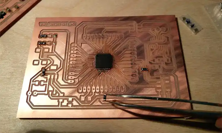
The process of DIY PCB etching involves the following steps:
1. Design and Prepare the PCB Layout: Use PCB design software to create the desired layout of your circuit. Ensure accurate placement of components and trace connections. Once the design is ready, print it on a suitable medium, such as a transparency film or specialized PCB transfer paper.
2. Prepare the Copper Clad Board: Cut a piece of copper clad board to the desired size for your PCB. Clean the board’s surface using steel wool or fine-grit sandpaper to remove any oxidation or impurities. Ensure that the board is free from dust and debris.
3. Transfer the PCB Layout: Place the printed layout onto the copper side of the board, aligning it correctly. Apply heat and pressure using a laminator or a heated iron to transfer the toner or ink from the printed layout onto the board’s surface. Allow the board to cool before proceeding.
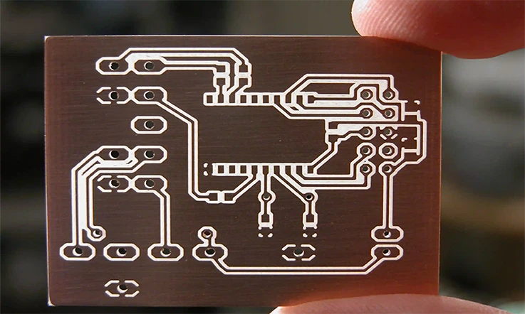
4. Etch the PCB: Prepare an etching solution, typically a mixture of ferric chloride or ammonium persulfate and water, following the manufacturer’s instructions. Wear protective gloves and goggles. Immerse the board into the etching solution and agitate it gently. Monitor the etching progress until all unwanted copper is dissolved, leaving only the desired circuit traces.
5. Rinse and Clean the PCB: Remove the board from the etching solution and rinse it thoroughly with water to halt the etching process. Use a scrub brush or sponge to remove any remaining toner or ink. Dry the board completely.
6. Remove the Toner or Ink: To remove the toner or ink from the PCB surface, soak it in an appropriate solvent, such as acetone or lacquer thinner. Gently scrub the board with a brush to remove the remaining toner or ink, revealing the copper traces.
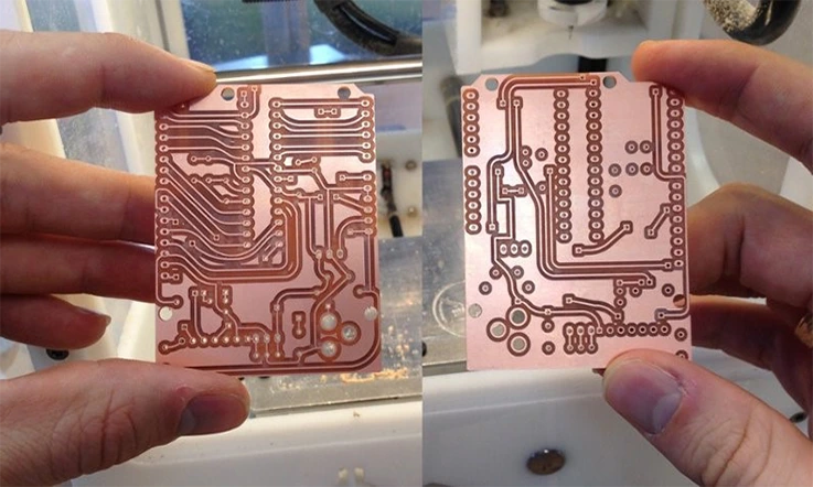
7. Inspect and Test the PCB: Carefully inspect the PCB for any defects or incomplete traces. Use a multimeter or continuity tester to verify the connectivity of the circuit. Make any necessary repairs or modifications if needed.
8. Apply Solder Mask and Silkscreen (optional): If desired, apply a solder mask to protect the copper traces and create a professional appearance. Additionally, you can add a silkscreen layer for labeling components or adding design elements.
It is important to note that DIY PCB etching requires proper safety precautions and adherence to guidelines. Follow all safety measures, such as working in a well-ventilated area, wearing protective gear, and disposing of chemicals appropriately.
Safety Measures While Undertaking PCB Etching
When undertaking PCB etching, it is crucial to prioritize safety and take appropriate measures to mitigate potential risks. The following guidelines should be adhered to:
1. Personal Protective Equipment (PPE): Always wear the necessary PPE, including safety goggles or glasses to protect your eyes from chemical splashes or flying debris. Gloves and an apron should be worn to shield your skin from corrosive chemicals.
2. Well-Equipped Workspace: Set up your workspace in a well-ventilated area to minimize exposure to hazardous fumes. Ensure that you have access to an eyewash station, a telephone for emergencies, and a fully stocked first aid kit nearby.
3. Proper Handling of Chemicals: Familiarize yourself with the properties and potential hazards of the chemicals used in the etching process. Follow the manufacturer’s instructions for storage, handling, and disposal of chemicals. Avoid contact with skin and eyes and work with chemicals in a controlled manner.
4. Power Tool Safety: If power tools are involved, such as drills or routers, exercise caution when operating them. Follow proper safety procedures, including wearing appropriate protective gear and ensuring the workspace is clear of any potential hazards.
5. Adequate Ventilation: Maintain good ventilation in the workspace to minimize the buildup of harmful chemical vapors. If necessary, use exhaust fans or work in a fume hood to remove fumes effectively.
6. Emergency Preparedness: Have a clear understanding of emergency procedures and escape routes in case of accidents or chemical spills. Keep emergency contact numbers readily available and ensure you know how to use the eyewash station and first aid supplies.
7. Seek Expert Guidance: If you are unsure about any aspect of the PCB etching process, consult with an experienced professional or seek guidance from knowledgeable resources. It is better to ask for assistance than to proceed with uncertainty.
By following these safety measures, you can reduce the risk of accidents, injuries, and chemical exposure during PCB etching, ensuring a safer working environment.
Why Choose JarnisTech for Your PCB Etching Solutions?
We understand your interest in engaging in the process of DIY PCB etching. It can be an enjoyable and educational experience, allowing you to acquire new skills. However, we also recognize that this endeavor can present challenges along the way.
At Jarnistech, we aim to provide comprehensive PCB etching solutions that set us apart from numerous other companies in the industry. Our commitment to delivering exceptional quality PCBs is matched by our dedication to providing outstanding customer care and efficient service.
By choosing us, you can benefit from several key advantages. Firstly, we prioritize saving our customers’ valuable time and hard-earned money. Through our streamlined processes and prompt delivery, we ensure a swift turnaround time without compromising on the quality of our products. Additionally, we strive to offer competitive quotes that are difficult to resist, providing our customers with cost-effective solutions.
Our overarching objective is to instill peace of mind in our valued clients. This commitment is evident throughout every aspect of our operations, from the quality of our PCBs to our customer-centric approach. We are dedicated to meeting and exceeding customer expectations, ensuring a positive experience throughout the entire engagement.
In summary, when choosing Jarnistech for your PCB etching needs, you can expect exceptional customer service, high-quality products, efficient delivery, and competitive pricing. We look forward to the opportunity to serve you and contribute to the success of your PCB projects.
Conclusion
PCB etching is a crucial step in the production of circuit boards. It is a process that requires precision and accuracy to ensure the final product functions as intended. As electronics continue to miniaturize and grow more complex, the etching process will continue to be a key part of circuit board manufacturing.
Printed circuit boards (PCBs) have been integral components of electronic systems for close to 100 years, demonstrating their sustained importance. With the ongoing miniaturization of electronics, demand rises annually for compact, high-density PCBs. Cutting-edge manufacturing technologies now enable smaller circuit boards than ever previously possible. While PCB fabrication requires various materials and processes, it fundamentally relies on Gerber files.
So what exactly are Gerber files, and how are they generated? In this guide, I’ll walk through everything PCB designers need to know about these critical files.
Gerber Files Definition
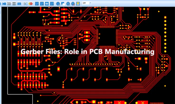
The Gerber file format serves as the de facto standard in the PCB manufacturing industry, analogous to generating a *.pdf file after designing graphics or text documents. Nearly all PCB designers, whether hobbyists or professionals, have used Gerber files at some point. The format itself is an ASCII file type.
The Gerber format evolved from printing and plotting applications where it was used to recreate images and graphics. Similarly, in PCB design, Gerber files convey all the critical data from the source PCB file – tracks, holes, clearances, etc. – as printable graphics. Leading PCB CAD software can export PCB projects as Gerber files. These programs typically employ the RS-274-X variant of the Gerber standard, as it handles data efficiently.
For PCB designers, producing industry-standard Gerber files is a crucial step before sending a board out for fabrication. The files package all the layered graphical information fabricators need to replicate the design as a physical PCB. Overall, the Gerber format bridges the gap between PCB design software and manufacturing capabilities. As PCB designers, being fluent in generating proper Gerber output ensures our boards can be manufactured smoothly and accurately.
A Gerber file uses a basic ASCII vector format and contains the following elements:
● Configuration settings.
● Macro and aperture definitions.
● Draw and flash command codes.
● XY coordinate data.
Each drill span and image layer of the PCB design is exported as a separate Gerber file from the source design. For a simple two-layer board, over eight files may be transmitted to the PCB manufacturer, potentially including:
● Copper layer image for the bottom of the board.
● Copper layer image for the top of the board.
● Solder mask and silkscreen images for the bottom and top.
● Drill files showing hole positions and functions.
Plated and non-plated holes are often separated into different files. A complete PCB fabrication data package provides the manufacturer with all necessary instructions, such as required machining processes and other specifications. The comprehensive information in the Gerber files enables the PCB fabricator to accurately replicate the designed board.
What Should Include In Gerber Files?
To generate comprehensive Gerber files for PCB manufacturing, the following layers and information should be included:
Signal layers: All active signal layers carrying electrical connectivity must be enabled to produce corresponding Gerber files.
Plane layers: Like signal layers, all power and ground plane layers should be enabled to output Gerber files. Planes provide low-impedance power distribution.
Keepout layer: The board outline and non-conductive keepout zones should be delineated on a layer to clearly define electrical boundaries.
Mechanical layers: Any mechanical layers used for board outlines, mounting holes, etc. need to be enabled for Gerber generation even if they contain no electrical data.
Overlays: Top and bottom silkscreen overlays with component designators and reference markings need outputting.
Board dimensions: Overall PCB dimensions should be noted on the keepout layer or overlays for manufacturing reference.
Layer stackup: The board’s material stackup must be documented on a mechanical layer to provide details like core thickness, prepreg type, etc.
Timestamping: Dating the Gerber files aids version control and assists with any troubleshooting.
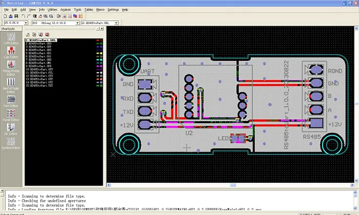
Verification: Use Gerber viewing software to validate file accuracy before release.
Thoroughly checking that the Gerber package contains all necessary fabrication data ensures the PCBs made match the intended design. Once validated, the files can be confidently transmitted to the manufacturer.
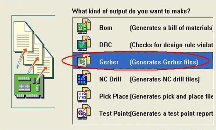
How to Generate the Gerber Files?
Generating Gerber files is a key part of the process of manufacturing printed circuit boards (PCBs) because these files provide all the necessary information about your PCB design to your manufacturer. Gerber files are a universally accepted standard for this kind of data.
The process of generating Gerber files varies slightly depending on the software you’re using, but the general steps are:
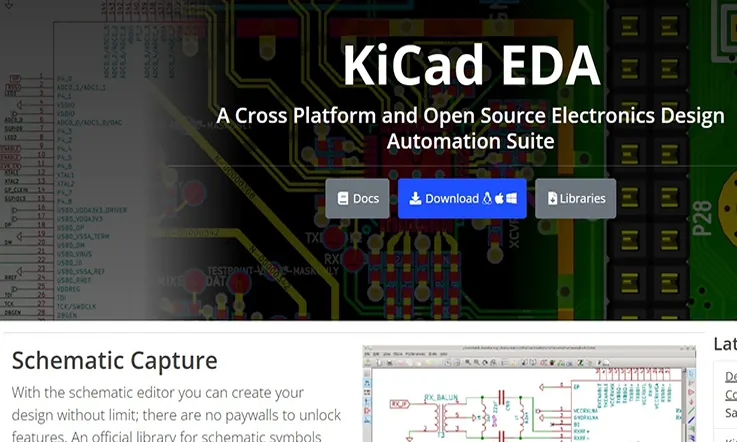
1. Design your PCB: You’ll first need to design your PCB with a software tool. There are many options available, including Eagle, KiCad, Altium Designer, and others.
2. Check your design: Before you can generate the Gerber files, you need to ensure that your design is correct and meets all necessary specifications. Most PCB software will have design rule checks (DRC) that can help with this.
3. Generate Gerber files: Once your design is finalized and checked, you can generate the Gerber files. The exact method for doing this will depend on your software, but it generally involves selecting an option like “Fabrication Outputs” or “CAM Processor” and then choosing the Gerber format. Note that you’ll usually need to generate a separate Gerber file for each layer of your PCB, including the copper, solder mask, and silkscreen layers.
4. Generate NC Drill Files: Alongside the Gerber files, you should also generate NC Drill files. These files are used to guide the drilling process during PCB manufacturing.
5. Inspect the Gerber files: After you’ve generated your Gerber files, it’s a good idea to check them using a Gerber viewer. This allows you to see exactly what your manufacturer will see and to check for any potential issues.
6. Send the Gerber files to your manufacturer: Once you’re satisfied with your Gerber files, you can send them to your manufacturer. They’ll use these files to manufacture your PCB.
Remember, generating Gerber files is a critical step in creating a successful PCB, so it’s important to take the time to get it right.
Kicad, Altium Designer and Eagle Software: How to Generate PCB Gerber Files?
As a PCB designer, we know it’s crucial to understand how Gerber file generation varies across design tools. Each program has its own workflow for producing the manufacturing data needed to get our boards fabricated. In this guide, we’ll share the specific steps I follow to create industry-standard Gerber files when I design PCBs with kicad, Altium Designer, and Eagle.
While the software packages differ, the end goal is the same – translating our schematics and layouts into the layered imaging information that PCB production facilities require. By carefully following the right file export procedures for each tool, we can ensure the Gerber files contain accurate fabrication data for every PCB layer. Before sending any board out for manufacturing, it’s essential that designers verify Gerber file integrity to avoid potential issues down the line. Knowing the ins and outs of generating proper Gerber output gives us confidence our boards will be produced as intended.
Kicad- Kicad Exporter Gerber
Here are the steps to generate Gerber files using Kicad:
1. Open the PCB project in Kicad. Go to File > Plot to open the plot dialog box.
2. Under “Plot Format” select “Gerber”
3. Enable the layers you want to output under “Layers to plot”. This typically includes:
● F.Cu (Top Copper Layer)
● B.Cu (Bottom Copper Layer)
● F.Mask (Top Solder Mask)
● B.Mask (Bottom Solder Mask)
● F.SilkS (Top Silkscreen)
● B.SilkS (Bottom Silkscreen)
● Edge.Cuts (Board Outline)
4. Under “Drill and Map Files” check the option to generate drill files.
5. Adjust other settings like output directory, file naming, units etc.
6. Click “Plot” to generate the Gerber and drill files.
7. The output folder will now contain the Gerber files, Excellon drill file, and drill map file.
8. Use a Gerber viewer to inspect the files before releasing to fabrication.
Following these steps in Kicad will produce the necessary Gerber manufacturing data from your PCB design, ready for sending to production.
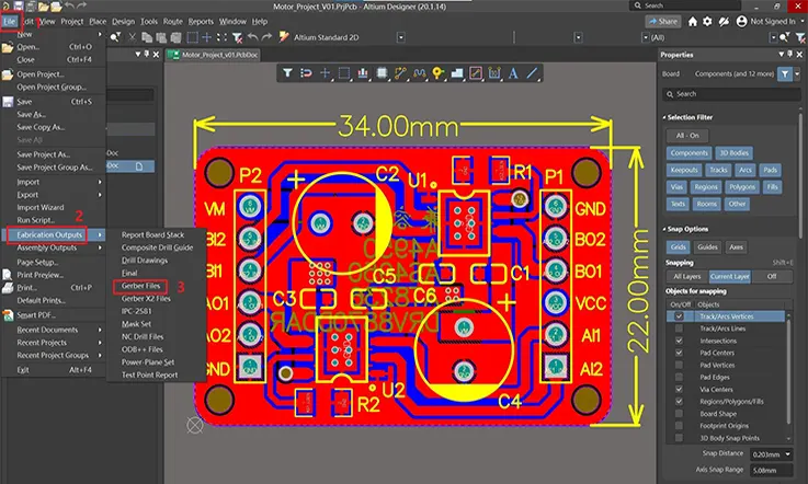
Altium Designer- Altium Gerber Files
Here are the steps to generate Gerber files using Altium Designer:
1. Open the PCB project in Altium Designer.
2. From the menu, select File > Fabrication Outputs > Gerber Files. This will open the Gerber settings window.
3. In the layers tab, select all the layers you need to generate Gerber files for. Typically this includes:
● Top and Bottom Copper Layers.
● Solder Mask Layers.
● Silkscreen Layers.
● Drill Drawing Layer.
● Board Outline Layer.
4. In the options tab, select the output directory and make any other adjustments to file naming, units etc.
5. Enable the “Generate Drill File” option to output the NC drill files.
6. Click on “Output All” to generate the Gerber and drill files. This may take some time depending on the board complexity.
7. The output folder will now contain the Gerber files, NC drill files and a Drill Map file detailing hole sizes and locations.
8. Use a Gerber viewer to inspect the files carefully before sending to fabrication.
Following these steps allows you to reliably produce industry-standard Gerber manufacturing data directly from your finished Altium PCB designs.
Eagle- Eagle Gerber Files
Here are the steps to generate Gerber files using Eagle CAD:
1. Open the PCB project in Eagle.
2. Run the CAM processor tool (File > CAM Processor).
3. In the CAM job, enable the following layers for Gerber output:
● op Copper
● Bottom Copper
● Solder Mask Top
● Solder Mask Bottom
● Silkscreen Top
● Silkscreen Bottom
● Board Outline
4. Check the “Use Route Commands” option.
5. Enable drill file output.
6. Set output directory and file naming preferences.
7. Click “Process Job” to generate the Gerber and drill files.
8. The output folder will contain the Gerber files (named per the layers), an Excellon drill file, and drill aid file detailing hole sizes and locations.
9. Use a Gerber viewer to verify the files before releasing to your PCB manufacturer.
Following these steps when using Eagle CAD will produce industry-standard Gerber files from your board design, containing all needed data for fabrication.
Gerber Files Play a Critical Role in PCB Manufacturing
Originally containing just basic configuration settings, macro definitions, and aperture sizes, Gerber files have evolved to encode more comprehensive fabrication data. While the core Gerber file format remains unchanged, the capabilities of PCB plotters and lasers have advanced significantly.
Modern PCB lasers still rely on the same Gerber file parameters to guide fabrication. However, the aperture limitations of earlier vector plotters no longer apply. Gerber data directs lasers on the precise locations and specifications for trace generation. Plotters translate the Gerber files into raster images to produce the PCBs.
Although Gerber file specifications continue to be enhanced, the format fundamentals persist for consistency. For the foreseeable future, this decades-old standard will likely experience only incremental changes, rather than a major overhaul. PCB manufacturers worldwide depend on Gerber files daily to translate design files into physical boards. Maintaining format continuity, while allowing measured improvements, helps sustain this vital manufacturing bridge.
Summary
The Gerber file format serves as the de facto standard for transferring information between PCB designers and manufacturers. Gerber files utilize the RS-274-X 2D ASCII format to convey all conductive, mechanical, text, and keepout layer data from the source PCB design, along with any necessary manufacturing notes.
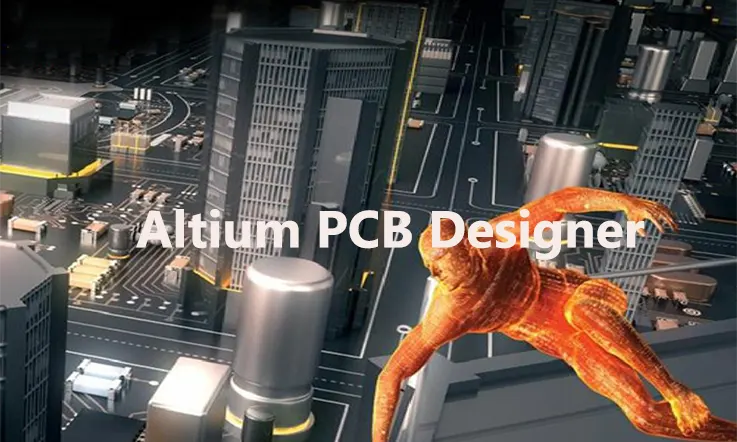
Are you interested in the field of electronics? If so, you might be familiar with Altium PCB, a prominent software used for designing printed circuit boards. For those who are unfamiliar, allow me to provide an in-depth analysis of this revolutionary technology. Whether you are a novice or well-versed in this software, you will undoubtedly find the unique aspects of Altium PCB fascinating. Join me as we explore the remarkable world of Altium PCB and its impact on the field of technology.
As an engineer, you may have experienced the challenges of designing a circuit board on a traditional piece of paper. Thankfully, Altium PCB was created to address these difficulties and enhance the efficiency of your work. This software enables you to create a printed circuit board using your computer, eliminating the need for manual drawings. With a wide array of tools at your disposal, Altium PCB empowers you to design not only visually appealing circuit boards but also intricate and detailed ones.
Altium PCB Design Software
Altium Designer is a popular Printed Circuit Board (PCB) design software widely used by engineers and designers for the creation of complex and high-quality electronic products. The software integrates a range of features and functionalities that make it a comprehensive tool for PCB design.
Key Features
Schematic Capture: This is a critical tool in Altium Designer that allows engineers to draw out their circuit designs before turning them into PCB layouts.
PCB Layout: This feature helps designers to lay out the physical aspects of their PCB. It includes tools for placing and moving components, routing traces, and more.
3D Visualization: Altium Designer provides a 3D visualization tool that allows designers to view their PCBs from different angles. This can help them spot potential issues that may not be visible in 2D.
Signal Integrity Analysis: This tool helps engineers ensure that their designs will function as expected by checking for potential signal integrity issues.
Real-time BOM Management: Altium Designer includes a bill of materials (BOM) management tool that updates in real time as you make changes to your design.
Component Libraries: A large library of components is available in Altium Designer, providing access to thousands of components with their footprints and schematics.
Design Rule Checking (DRC): DRC is a powerful feature that checks your PCB design against a set of rules you define, helping to ensure your design meets necessary specifications and standards.
Learning Altium Designer
Like any complex software, learning to use Altium Designer effectively takes time and practice. Here are some tips to get you started:
Tutorials and Guides: Altium provides a range of tutorials and guides on their website. These can be a great place to start if you’re new to the software.
Community Forums: Altium has a strong user community, and their forums can be a valuable resource for getting help and advice.
raining Courses: There are also several online training courses available that can help you learn the ins and outs of Altium Designer.
Practice: The best way to learn is by doing. Try designing a simple PCB to start with and gradually take on more complex projects as you become more comfortable with the software.
Benefits of Altium PCB Design Software
Altium PCB design software offers several notable benefits for engineers and designers in the field of electronics. Here are some key advantages of using Altium PCB:
User-Friendly Interface
Altium PCB provides an intuitive and user-friendly interface, making it accessible to both novices and experienced professionals. The software’s layout and tools are designed to streamline the design process and improve productivity.
Comprehensive Design Tools
Altium PCB offers a wide range of design tools that empower engineers to create intricate and detailed circuit board designs. These tools include schematic capture, component library, design rule checks, and advanced routing options, among others. The comprehensive toolset caters to various design requirements and ensures high-quality output.
Enhanced Collaboration
Altium PCB supports seamless collaboration between team members. It allows multiple designers to work on the same project simultaneously, enabling efficient sharing of design files, annotations, and comments. This collaborative environment fosters teamwork and accelerates the design process.
Integration with Other Software
Altium PCB integrates smoothly with other software commonly used in the electronics industry, such as mechanical design tools and simulation software. This integration enables a seamless transfer of data between different software platforms, ensuring compatibility and facilitating a more holistic design approach.
Design Rule Checks (DRC)
Altium PCB incorporates powerful design rule checks, which automatically verify the design against predefined manufacturing rules and constraints. This feature helps identify potential errors or design flaws early in the process, reducing the chance of costly mistakes and ensuring compliance with manufacturing guidelines.
Component Library and Management
Altium PCB includes an extensive component library with a vast collection of pre-designed electronic components. This library saves time and effort by providing ready-to-use components, reducing the need for manual component creation. Additionally, Altium PCB allows users to manage and update their component libraries, ensuring accurate and up-to-date design data.
Real-Time 3D Visualization
Altium PCB offers real-time 3D visualization capabilities, allowing designers to view their circuit boards in a three-dimensional representation. This feature aids in visualizing the final product, verifying component placements, and detecting potential mechanical conflicts early in the design phase.
Manufacturing Documentation
Altium PCB generates comprehensive manufacturing documentation, including precise bill of materials (BOM), assembly drawings, and fabrication outputs. This documentation streamlines the manufacturing process and ensures accurate communication between designers and manufacturers.
Ongoing Support and Community
Altium provides ongoing support and a vibrant user community for its PCB design software. Users can access extensive documentation, video tutorials, forums, and knowledge bases to seek assistance, exchange ideas, and stay updated on the latest industry trends.
Disavantages of Altium PCB Design Software
While Altium PCB design software offers numerous benefits, it also has certain limitations and disadvantages that users should be aware of. Here are some potential drawbacks of using Altium PCB:
Cost: Altium PCB is a professional-grade software, and as such, it comes with a significant price tag. The cost of licensing Altium PCB may be prohibitive for individual users, small businesses, or hobbyists with limited budgets.
Steep Learning Curve: Altium PCB has a rich set of features and tools, which can lead to a steep learning curve for new users. It may take time and effort to become proficient in utilizing the software’s capabilities fully. While Altium provides resources and documentation, the initial learning process can be challenging.
Resource Intensive: Altium PCB can be resource-intensive in terms of system requirements. The software demands a powerful computer with ample processing power, memory, and storage. Users with older or less capable hardware may experience performance issues or limitations.
Complexity for Simple Designs: Altium PCB is designed to handle complex and advanced circuit board designs. For users working on relatively simple or straightforward projects, the software’s extensive feature set may feel overwhelming or unnecessary. It might be more efficient to use a simpler and more lightweight software solution in such cases.
Limited Platform Support: Altium PCB primarily runs on Windows operating systems, limiting its availability to users of other platforms such as macOS or Linux. Although workarounds like virtual machines or emulators exist, they may not provide the same level of performance and integration as the native Windows version.
Lack of Advanced Simulation Capabilities: While Altium PCB offers basic simulation capabilities, it may not be as comprehensive as specialized simulation software packages. Users requiring in-depth circuit analysis and simulation may need to integrate Altium PCB with additional simulation tools or consider alternative software solutions.
Dependency on Altium Ecosystem: Altium PCB is tightly integrated with the Altium ecosystem, which includes other software tools and services. While this integration can be beneficial, it also means that users may become dependent on the Altium ecosystem for their design workflow. This can limit flexibility and make it challenging to transition to or collaborate with users of different software platforms.
It’s worth noting that some of these disadvantages can be mitigated or addressed through alternative software choices, additional tools, or by considering individual project requirements. It’s essential to evaluate your specific needs and constraints before deciding on the most suitable PCB design software for your purposes.
Conclusion
By leveraging Altium PCB, engineers can benefit from a range of features that streamline the design process. These include advanced schematic capture capabilities, a comprehensive component library, intuitive design rule checks, and extensive routing options. The software’s schematic capture function allows users to create clear and organized circuit diagrams, making it easier to understand and modify the design. Additionally, Altium PCB offers a vast library of components, enabling designers to quickly access and integrate various electronic parts into their projects.
Therefore, Altium Designer is a comprehensive PCB design software packed with many powerful features. It’s used by professionals worldwide and is known for its flexibility and efficiency. However, like any advanced tool, it requires some time and effort to master. With the right resources and plenty of practice, you can become proficient in using Altium Designer and create high-quality PCB designs.
In the manufacturing process of printed circuit boards (PCBs), various techniques are employed to shape and refine the blank PCBs before they are ready for component assembly. One such essential step is milling, which involves the removal of excess material from the blank PCB to achieve the desired shape, dimensions, and features. Milling plays a crucial role in PCB fabrication, ensuring precision, accuracy, and functionality of the final product.
By understanding the purpose and advantages of milling blank PCBs, manufacturers, designers, and electronics enthusiasts can gain valuable insights into this critical step, enabling them to make informed decisions and optimize their PCB fabrication processes. So, let’s dive into the details and unravel the significance of milling in PCB manufacturing.
What is Blank PCB?
A blank PCB (Printed Circuit Board) refers to a circuit board that has been manufactured but does not have any electronic components or traces on it. It is essentially a bare board without any circuitry or functionality. Blank PCBs are typically used in the electronics industry as a starting point for designing and creating electronic devices.
The manufacturing process of a blank PCB involves several steps. First, a layer of copper is applied to the board, which serves as the conductive material for the circuitry. Then, a layer of protective material called solder mask is applied to prevent accidental short circuits and to insulate the copper traces. Finally, holes are drilled into the board to facilitate component placement and connection.
Once the blank PCB is ready, it can be used for various purposes. Designers and engineers can mount electronic components such as resistors, capacitors, integrated circuits (ICs), and connectors onto the board to create a functioning electronic device. The components are soldered onto the copper pads and connected using conductive traces on the board, forming the desired circuitry.
Blank PCBs provide a foundation for custom electronic designs, allowing for flexibility and customization in creating specific electronic systems or prototypes. They are commonly used in industries such as consumer electronics, telecommunications, automotive, aerospace, and many others.
Blank PCB Materials
Here are some common blank PCB materials:
FR-4: This is the most common and inexpensive material for PCBs. FR-4 is a composite of woven fiberglass cloth with an epoxy resin binder. It has good mechanical strength and is suitable for most general purpose applications.
CEM-1: Woven cotton paper substrate with epoxy resin. It has better thermal properties than FR-4 but lower mechanical strength. Used for RF and high frequency applications.
Rogers: A variety of high frequency PCB materials by Rogers Corporation with dielectric constants tailored for high speed digital and RF applications. Common Rogers materials include RO4003, RO4350B, RO4835.
Alumina:Ceramic PCBs with high thermal conductivity used for power circuits and high temperature operation. More expensive than FR-4.
Teflon/PTFE: Woven fiberglass reinforced fluoropolymer with excellent chemical resistance and dielectric properties. Used for high frequency RF boards.
The choice depends on electrical, thermal, mechanical and cost requirements. FR-4 is suitable for most general applications, while more advanced materials are used for specialized high speed or high frequency needs. The PCB fab house can advise on blank material selection.
Blank PCB Color
Blank PCBs typically have a characteristic color that is determined by the base material used for the substrate. The most common color for blank PCBs is typically light yellow or tan. This color comes from the fiberglass-reinforced epoxy resin material (FR-4) that is commonly used for the substrate. FR-4 has a natural yellowish color due to the presence of the fiberglass reinforcement.
While light yellow is the most common color, it’s important to note that blank PCBs can also be found in other colors, such as light green, blue, or even black. These variations in color can be attributed to different formulations of the substrate material or the application of additional coatings or finishes.
It’s worth mentioning that the color of blank PCBs is primarily for aesthetic purposes and does not impact the functionality or performance of the board. The color may vary depending on the manufacturer or specific requirements of the project.
Why Blank PCB Used for Milling?
A blank Printed Circuit Board (PCB) is used for milling because the process involves the mechanical removal of copper layers to create an electrical circuit based on a digital design. This is why the PCB starts as a “blank”, meaning it’s fully coated with a layer of copper on one or both sides.
A few reasons why a blank PCB is used for milling include:
Customization: Milling allows for the creation of highly customized PCB designs. Starting from a blank PCB means that the design can be tailored to the exact specifications of the user.
Rapid Prototyping: If you want to test a design concept quickly, PCB milling is a great option. You can start with a blank PCB, mill your design, and have a functional prototype within a short time.
Cost-Effective for Small Batches: For large-scale production, methods like PCB etching might be more cost-effective. However, for small batches or single boards, milling can be more economical because it doesn’t require the creation of an etching mask.
Reduced Waste: With milling, only the unwanted copper is removed. This could result in less waste compared to methods like etching, where the entire copper layer is first applied and then largely removed.
No Chemicals Required: Unlike etching methods, which use chemicals to remove unwanted copper, milling is a mechanical process that doesn’t require potentially harmful chemicals.
Remember that while milling has its advantages, it also has limitations. It might not be suitable for very complex or high-density PCB designs, and the accuracy is somewhat dependent on the quality of the milling machine used. Each method has its place, and the choice between them depends on the specific requirements of the PCB design project.
What is Blank PCB Milling?
Blank PCB milling is a process for creating custom printed circuit boards (PCBs) by using a computer-controlled milling machine to cut away copper from a blank PCB laminate. It involves the following main steps:
● Design the PCB layout in CAD software and export the Gerber files.
● Secure a blank PCB substrate, usually single or double sided FR-4 or copper clad laminate.
● Align and clamp the blank PCB on the milling machine bed.
● Load the Gerber files into the milling machine software. This converts the PCB layers into toolpaths for the milling bit.
● Perform tool change to load the appropriate end mill cutter. Small end mills are used to carve fine traces.
● Perform surface profiling to account for PCB surface irregularities. This ensures proper depth control.
● Run the milling program which mills away copper from the blank PCB to isolate traces and create pads/vias based on the PCB design files.
● Clean away milling debris and inspect the milled PCB under microscope.
Milling provides quicker turnaround time than chemical etching and allows creating fully custom PCBs in a small lab setup. But the equipment cost is higher than etching.
Useful Tips for Blank PCB Milling
Use fine end mills for tracing – Single flute carbide end mills down to 0.1mm work well for PCB traces. Multi-flute end mills are preferred for milling large copper areas.
Minimize runout – Make sure the end mill is tightly secured and has minimal runout. Otherwise it will affect milling quality.
Use sacrificial substrate – Attach a sacrificial fiberglass or acrylic layer on top of the PCB blank during milling. This helps preserve the end mill life.
Optimize feed and speed – The milling feed rate and spindle RPM have to be optimized based on the end mill size to get clean edges. Faster feed and lower RPM for smaller tools.
Use climb milling – Where the cutter rotation opposes the feed direction. It gives better results than conventional milling for PCBs.
Secure PCB blank – Use vacuum hold down or dabs of glue to securely hold the PCB blank in place during milling.
Clear debris – Periodically clear away milling debris using brushes and compressed air to avoid re-cutting.
Limit trace width – Keep trace widths greater than the end mill diameter for cleanest cutting.
Apply solder mask – A solder mask coating will protect the milled traces from oxidation and damage.
Proper fixturing, cutter selection, speeds/feeds and debris control are key to getting good results from PCB milling.
Conclusion
Milling blank PCBs serves multiple purposes and offers significant advantages in the PCB manufacturing process. From achieving precise shapes and dimensions to facilitating component fitment, design flexibility, and signal integrity, milling plays a crucial role in producing high-quality PCBs. It allows for customization, improves thermal management, reduces weight, and optimizes manufacturing costs. By recognizing the purpose and advantages of milling, PCB designers and manufacturers can harness its potential to create superior and reliable electronic products.
Printed Circuit Board (PCB) panelization is a critical step in the electronics manufacturing process that plays a significant role in optimizing efficiency and cost-effectiveness. As electronic devices become more compact and complex, the demand for smaller and more intricate PCB designs continues to rise. To meet these demands, manufacturers employ panelization techniques to efficiently produce multiple PCBs on a single panel.
This article aims to explore the impact of panelization design on PCB fabrication, emphasizing its importance and offering valuable insights for achieving optimal design.
What is PCB Panelization?
PCB panelization is a manufacturing technique that involves producing multiple smaller boards interconnected as a single array, facilitating efficient movement through the assembly line. Depanelization allows individual boards to be separated from the array for packaging or installation into products. Another approach involves adding a processing edge around each board to increase its width for compatibility with the assembly line.
To fully leverage the advantages of mass production through panelization, it is crucial to consider the following design factors:
PCB array strength: Achieving a balance between easy depanelization and maintaining array integrity during production is essential. Increasing the number of boards per array enhances strength and reduces vibration.
Component layout: Careful consideration should be given to the placement of components and connectors, particularly those extending beyond the board’s edge. This is especially important for sensitive SMT components located near the board’s edge.
PCB shape: The shape of the board can complicate the panelization process. Ideally, rectangular boards are preferred. However, if the board has a complex shape, alternating images from 90° to 180° can help optimize space on a panel. Utilizing a CAD program can assist in fitting unusually shaped boards into an array.
Tooling holes: Arrays and break-away processing edges can provide space for tooling holes, which are crucial for automated testing on the assembly line.
By considering these design considerations, PCB panelization can enhance the efficiency of fabrication and assembly processes, enabling streamlined mass production and improved overall product quality.
PCB Panelization Design Method
When it comes to PCB panelization design, there are several methods and techniques that can be employed to achieve optimal results. Here are some commonly used approaches:
Grid-Based Panelization
This method involves arranging PCBs in a grid pattern on a panel. The boards are evenly spaced and aligned to facilitate efficient manufacturing and assembly processes. Grid-based panelization is straightforward and allows for easy handling and depanelization.
Tab Routing
Tab routing involves adding small tabs or bridges between individual PCBs on a panel. These tabs provide mechanical support during manufacturing and allow for easy separation of the boards after assembly. Tab routing is often used when the PCBs are of a similar size and shape.
Breakaway Rails
Breakaway rails are additional sections of material added around the perimeter of the panel, creating a larger panel size. The individual PCBs are located within these rails and can be easily separated after manufacturing. Breakaway rails provide stability and support during fabrication and assembly.
Mouse Bite Panelization
In this method, small perforations or mouse bites are created between individual PCBs, allowing for easy separation. Mouse bites are small, partially cut sections that can be easily snapped or broken to separate the boards. This method is commonly used when space constraints are a concern.
V-Scoring
V-scoring involves creating V-shaped grooves on the panel between the individual PCBs. These grooves allow for easy separation by bending the panel along the scored line. V-scoring is particularly useful when working with larger boards or when a clean and precise separation is desired.
Panel Array Design
In this approach, multiple PCBs of the same design are replicated and placed side by side on a larger panel. This method maximizes production efficiency by allowing for simultaneous manufacturing and assembly of multiple boards.
The choice of panelization design method depends on factors such as PCB size, quantity, shape, assembly requirements, and desired level of automation. It is important to consider the specific needs of the project and consult with PCB manufacturing experts to determine the most suitable panelization method for optimal fabrication and assembly results.
V-score vs. Tab Routing PCB Panels
The decision of whether to use V-scoring or tab routing for a PCB panel depends on the specific design considerations for that board. While these two methods are not mutually exclusive and can be combined when appropriate, there are tradeoffs to weigh for each one.
V-scoring is generally a faster process than tab routing, requiring less time on the routing machine. However, tab routing may provide higher edge quality, with only small laminate nubs that can be easily sanded off to leave smooth edges. In contrast, V-scoring tends to leave rougher edges across the board.
The shape of the PCBs in the panel should be evaluated when selecting the panelization method. V-scoring performs well for square or rectangular boards, while tab routing accommodates more irregular board outlines.
If the design has components placed near the board edges, tab routing may be preferable to avoid damaging these components, provided the tabs themselves are not positioned too close to the edges.
Finally, V-scoring is the more material-efficient technique, producing less waste than tab routing. This can significantly reduce costs on a per board basis.
By weighing these factors against the specific needs of the PCB design, engineers can make an informed decision between V-scoring and tab routing to optimize the panelization process. A combination approach is also possible when elements of both methods would benefit the board layout.
When is PCB Panelization Required?
PCB panelization is typically required in the following situations:
Mass Production: When producing PCBs in large quantities, panelization is necessary to optimize the manufacturing process. By arranging multiple boards on a single panel, efficiency is improved, as it allows for simultaneous fabrication and assembly of multiple PCBs.
Cost-Effectiveness: Panelization offers cost savings in terms of materials, setup, and handling. By maximizing the use of manufacturing equipment and minimizing material waste, panelization helps reduce production costs, making it a preferred method for cost-effective PCB manufacturing.
Assembly Line Compatibility: PCBs that need to be processed through automated assembly lines often require panelization. By designing the panel layout to match the assembly line’s capabilities, it ensures smooth and efficient automated assembly processes.
Space Optimization: Panelization is useful when trying to optimize the utilization of available space on a production panel. By arranging PCBs strategically, designers can maximize the number of boards that can fit on a single panel, minimizing wasted space.
Handling and Transportation: Panelization simplifies the handling and transportation of PCBs. By keeping multiple boards connected on a panel, they can be easily moved as a single unit, reducing the risk of damage or misplacement during transit.
Depanelization Requirements: If individual PCBs need to be separated from the panel after fabrication and assembly for packaging or installation purposes, panelization is necessary. It allows for controlled and efficient depanelization processes, ensuring the integrity of the individual boards.
It is important to consider the specific production requirements, quantity, and desired outcomes when determining whether PCB panelization is necessary. Consulting with PCB manufacturers and considering factors such as manufacturing capabilities, cost-efficiency, and logistics can help determine the need for panelization in a particular project.
Design Considerations for PCB Panelization
When designing PCB panelization, there are several important considerations to take into account to ensure a successful and efficient manufacturing process. Here are some key design considerations for PCB panelization:
Board Orientation and Alignment
Ensure that the PCBs are properly aligned and oriented within the panel. Consistent alignment helps maintain uniformity throughout the manufacturing process and facilitates accurate component placement and assembly.
Panel Size and Material
Determine the appropriate panel size based on the PCB dimensions and manufacturing requirements. Consider the material used for the panel, such as FR-4 or aluminum, and its compatibility with the PCB fabrication and assembly processes.
Spacing and Clearances
Provide adequate spacing between PCBs on the panel to prevent electrical and mechanical interference. Consider the clearance requirements for components, connectors, and traces that extend beyond the board edges. Adhere to design rules and industry standards to ensure proper functionality and reliability.
Tooling Holes and Fiducial Marks
Incorporate tooling holes into the panel design to facilitate accurate registration and alignment during manufacturing processes, such as drilling, routing, and assembly. Include fiducial marks for automated optical inspection (AOI) and component placement accuracy.
Breakaway Tabs or V-Grooves
If using breakaway tabs or V-grooves for depanelization, carefully design their placement to ensure easy separation without damaging the PCBs. Consider the size and quantity of tabs or grooves needed for proper mechanical support during manufacturing and easy separation afterward.
Panelization Method Selection
Choose the most suitable panelization method based on the PCB design and manufacturing requirements. Consider factors such as board size, shape, assembly process, and depanelization needs. Evaluate the advantages and limitations of different panelization methods to optimize efficiency and minimize waste.
Design for Assembly (DFA)
Design the panelization layout with assembly in mind. Group components with similar functionalities or assembly processes together to minimize assembly time and improve efficiency. Consider the accessibility of components for automated assembly equipment, such as pick-and-place machines.
Design for Testing
Plan for efficient testing and inspection of the PCBs within the panel. Ensure that test points are accessible and properly positioned for automated or manual testing methods. Consider the placement of test pads, test points, or test vias for electrical testing and debugging purposes.
Documentation and Communication
Clearly document and communicate the panelization design to PCB manufacturers and assembly partners. Provide comprehensive manufacturing instructions, including panelization drawings, assembly data, and any specific requirements or considerations for successful production.
By considering these design considerations during the PCB panelization process, you can optimize the manufacturing efficiency, assembly quality, and overall success of your PCB production. Collaborate closely with PCB manufacturers and assembly partners to ensure alignment with their capabilities and requirements.
How to Process the PCB Panelization design?
The process of PCB panelization design involves several key steps to ensure a successful outcome. Here is a general outline of the process:
1. Determine Panel Size and Quantity: Start by determining the desired panel size based on the PCB dimensions and manufacturing capabilities. Consider factors such as machine limitations, handling requirements, and production efficiency. Decide on the number of PCBs to be included in each panel based on production volume and cost considerations.
2. Define Panelization Method: Choose the appropriate panelization method that suits your project requirements. Consider factors such as board size, shape, assembly process, and depanelization needs. Common methods include grid-based panelization, tab routing, breakaway rails, mouse bite panelization, V-scoring, or panel array design.
3. Create Panelization Layout: Using a PCB design software or a dedicated panelization tool, create a panelization layout that arranges the PCBs on the panel according to the chosen method. Take into account the required spacing between boards, alignment, and any additional features like tooling holes or fiducial marks. Ensure that the layout adheres to design for manufacturability (DFM) guidelines.
4. Consider Component Placement: Pay attention to component placement on the PCBs within the panel. Avoid placing sensitive components near the panel edges or areas prone to stress during depanelization. Ensure proper clearance for connectors and other components that extend beyond the board edges.
5. Verify Design Rules and Constraints: Before finalizing the panelization design, run design rule checks (DRC) to ensure that the layout conforms to manufacturing and assembly requirements. Verify that there are no violations related to spacing, copper clearances, solder mask, or silkscreen markings.
6. Generate Panelization Files: Once the panelization design is complete, generate the necessary files for manufacturing. This usually includes Gerber files, NC drill files, assembly data, and any additional documentation or instructions required by the manufacturer.
7. Collaborate with PCB Manufacturer: Engage in communication and collaboration with the chosen PCB manufacturer. Share the panelization design files and discuss any specific requirements or recommendations. Seek their expertise to ensure the design is optimized for their manufacturing capabilities.
8. Review and Iteration: Review the panelization design with the manufacturer and address any feedback or modifications required. Iterate on the design if necessary to achieve the desired manufacturability, assembly efficiency, and cost-effectiveness.
By following these steps and collaborating closely with the PCB manufacturer, you can effectively process the PCB panelization design and ensure a smooth transition from design to production.
The Effect of Panelization Design on PCB Fabrication and Assembly
Panelization is an important aspect of Printed Circuit Board (PCB) manufacturing that involves the process of arranging multiple PCBs onto a larger board, or panel, during fabrication. The panel is then broken apart into individual PCBs after assembly. This process allows for the simultaneous fabrication and assembly of multiple PCBs, improving overall efficiency and reducing costs. However, the design of the panel can influence various factors in PCB fabrication and assembly, including cost, manufacturability, and reliability.
Efficiency and Cost-Effectiveness
Panelization design can significantly influence the efficiency and cost-effectiveness of PCB production. A well-designed panel can maximize the number of PCBs on a single panel, reducing material waste and lowering production costs. Furthermore, by allowing for the simultaneous processing of multiple boards, panelization can increase production speed and reduce labor costs.
Manufacturability
The design of the panel can also affect the manufacturability of the PCBs. For instance, boards that are too closely spaced may be difficult to route or may result in damaged boards when depaneling. On the other hand, too much space between boards can lead to wasted material and increased costs. Additionally, the panel design should also consider aspects such as the placement of fiducial marks and tooling holes, which can influence the accuracy and ease of assembly.
Reliability
Panelization design can impact the reliability of the final PCBs. For example, inadequate spacing or poorly designed break-off tabs can lead to damage during depaneling, potentially affecting the functionality and reliability of the PCBs. Moreover, the panel design should ensure that it can withstand the stresses of assembly processes, such as soldering and component placement, without warping or breaking.
Design for Manufacturability (DFM)
Panelization is an important aspect of Design for Manufacturability (DFM) in PCB production. DFM involves designing the PCB in a way that optimizes its manufacturability, considering factors such as ease of fabrication, assembly, testing, and cost-effectiveness. A well-designed panel can improve all these aspects, leading to a more efficient and cost-effective production process.
Therefore, panelization design plays a crucial role in PCB fabrication and assembly, affecting factors such as efficiency, cost-effectiveness, manufacturability, and reliability. Therefore, it’s important to carefully consider the design of the panel in the early stages of the PCB design process.
Conclusion
The significance of panelization design on PCB fabrication and assembly cannot be overstated. A carefully planned panelization design has a profound impact on the manufacturing process, improving efficiency, assembly, testing, and resource utilization. By integrating the specific requirements of PCB fabrication and assembly into the design process, engineers can achieve a streamlined and cost-effective production, resulting in high-quality PCBs suitable for a wide range of applications.
At JarnisTech, we are proud to offer our exceptional PCB panelization services to a global customer base. With our highly skilled and experienced team of professionals, we assure you that all your PCB panelization needs will be catered to with utmost care and precision. Whether you require panelization for small-scale projects or large-scale production, we have the expertise to deliver outstanding results. Contact us today to request a quote and experience the quality and efficiency of our PCB panelization services.
BGA solder joint inspection is a crucial quality control process that involves visual and X-ray examination of solder joints. Its primary purpose is to ensure the high quality and reliability of these joints. The inspection helps identify various defects such as cold solder joints, bridging defects, voiding defects, and solder balling defects.
However, due to the intricate nature and irregular shape of solder joints, visual inspection alone is challenging and insufficient. Consequently, this article aims to highlight the effectiveness of X-ray imaging as a preferred method for BGA solder joint inspection.
Now, let us delve into an exploration of the common BGA inspection methods before understanding why X-ray imaging stands out as a highly effective approach.
Some Common Methods Used to Inspect a BGA Solder Joint
Inspecting a Ball Grid Array (BGA) solder joint can be a technical and complicated task because the solder balls are not directly visible. It requires specialized equipment and trained personnel to accurately assess the quality of the joint. Here are some common methods used to inspect a BGA solder joint:
1. X-Ray Inspection
X-ray inspection is the most common method used for inspecting BGA solder joints. This non-destructive testing method can detect soldering defects like solder bridges, voids, or missing balls.
There are two types of X-ray systems: 2D and 3D.
● 2D X-Ray: This method provides a top-down view of the BGA, which can be useful for identifying gross defects. However, it may not reveal problems with individual balls that are hidden by others.
● 3D X-Ray (CT Scan): This method provides a three-dimensional view of the BGA, allowing for a more detailed inspection. This can reveal defects that may not be visible in a 2D X-ray.
2. Acoustic Micro Imaging (AMI)
AMI uses ultrasound technology to inspect solder joints. The ultrasound waves can penetrate the package and reflect back to create an image of the joints. This can reveal voids, cracks, and delaminations that may not be visible using X-ray inspection.
3. Endoscopic Inspection
Endoscopic inspection involves using a small camera to visually inspect the solder joints. This method can reveal defects on the surface of the solder balls, but it doesn’t provide information about the interior of the joints.
4. Destructive Testing
In some cases, it may be necessary to use destructive testing methods to inspect BGA solder joints. This could involve de-soldering the BGA and inspecting the individual solder balls. While this method can provide detailed information about the joints, it destroys the BGA in the process and is typically used for failure analysis rather than routine inspection.
Remember, each of these methods has its strengths and weaknesses, and the best approach often involves using a combination of them. It is also important to have trained personnel conduct these inspections to ensure accurate results.
What is a BGA X Ray Machine?
A BGA X-ray machine, also known as a BGA X-ray inspection system or BGA X-ray system, is a specialized equipment used for the inspection and analysis of Ball Grid Array (BGA) solder joints. It employs X-ray imaging technology to provide detailed and non-destructive visualization of the internal structures and connections within BGA packages.
The BGA X-ray machine typically consists of the following key components:
X-ray Source: It generates X-ray radiation that passes through the BGA package and is detected on the other side. The X-ray source can be a microfocus X-ray tube or a more advanced technology like a sealed X-ray tube or an X-ray generator.
Detector: The X-ray detector captures the X-ray radiation that passes through the BGA package. It may utilize technologies such as phosphor screens, flat-panel detectors, or complementary metal-oxide-semiconductor (CMOS) sensors. The detector converts the X-ray radiation into visible images or digital signals for analysis.
Control System: This system manages and controls the operation of the BGA X-ray machine. It includes software interfaces, user controls, and settings for adjusting X-ray parameters such as voltage, current, exposure time, and image capture settings.
Manipulation Mechanism: The BGA X-ray machine may have a motorized stage or a manipulator that allows precise positioning and rotation of the BGA package during the inspection process. This enables capturing X-ray images from different angles and viewpoints.
Imaging and Analysis Software: The software associated with the BGA X-ray machine provides tools for image acquisition, enhancement, measurement, and analysis. It allows operators to examine the X-ray images, identify potential defects or anomalies in the solder joints, and make informed decisions based on the inspection results.
The BGA X-ray machine is specifically designed to address the challenges of inspecting BGA solder joints, which are hidden beneath the package and not easily visible through traditional visual inspection methods. It enables thorough examination of solder quality, joint integrity, voiding, bridging, and other potential defects, helping to ensure the reliability and quality of electronic assemblies that utilize BGA components.
BGA X ray Machine Working Principle
A BGA X-ray machine works by utilizing X-ray imaging technology to penetrate the Ball Grid Array (BGA) package and capture detailed images of the internal structures and solder joints. The process can be summarized in the following steps:
Preparation: The BGA package to be inspected is prepared by ensuring it is properly positioned and securely held in place within the X-ray machine. This may involve using a manipulator or motorized stage to achieve precise alignment for accurate imaging.
X-ray Generation: The X-ray machine produces X-ray radiation using an X-ray source, which is typically a microfocus X-ray tube. The X-ray source emits a controlled beam of X-rays towards the BGA package.
X-ray Penetration: The X-ray beam passes through the BGA package, interacting with the materials it encounters, including the solder joints, substrate, and other internal components. The X-rays can penetrate the package due to the different absorption rates of the materials.
X-ray Detection: On the opposite side of the BGA package, there is an X-ray detector. The detector captures the X-rays that have passed through the package. The detector can be a phosphor screen, a flat-panel detector, or a CMOS sensor, depending on the specific X-ray machine.
Image Conversion: The X-ray detector converts the captured X-rays into visible images or digital signals. Phosphor screens emit visible light when exposed to X-rays, which can be captured using a camera. Flat-panel detectors and CMOS sensors directly convert X-rays into digital signals.
Image Analysis: The captured X-ray images or digital signals are processed and analyzed using specialized software associated with the X-ray machine. The software provides tools for image enhancement, measurement, and analysis. Operators can examine the images to identify potential defects or anomalies in the solder joints, such as voids, bridging, or insufficient solder.
Inspection and Evaluation: Based on the analysis results, operators can make informed decisions regarding the quality and reliability of the solder joints. They can determine if the solder joints meet the required standards or if any further actions, such as rework or repair, are necessary.
The BGA X-ray machine’s ability to penetrate the package and provide internal imaging enables comprehensive inspection of the solder joints, which are otherwise hidden from view. This non-destructive inspection method helps ensure the integrity and reliability of electronic assemblies that incorporate BGA components.
Which is the Best Method for the Inspection of a Solder Joint?
There is no universally superior method for BGA inspection, as each approach possesses its own advantages and disadvantages. The selection of a suitable method depends on the specific defects to be detected and the type of solder joints under inspection.
For instance, if the objective is to identify defects such as solder voids or closed circuits, visual inspection proves to be a viable method. Visual inspection allows for direct observation of the solder joints, enabling detection of surface-level irregularities.
When considering the use of an X-ray machine for BGA inspection, it is essential to understand the various types of defects that can be detected through this method. X-ray machines are primarily employed to identify voiding defects, wherein excess solder is not adequately deposited on the substrate. This specific defect type can only be accurately detected using X-ray imaging.
In addition to voiding defects, X-ray machines can also identify other solder joint issues such as cold solder joints and bridging defects. Cold solder joints occur when the solder paste does not receive sufficient heat or pressure during the soldering process. While infrared cameras can also detect this defect, an X-ray machine can be utilized for its identification as well.
Bridging defects, on the other hand, manifest when the solder paste extends between the package and the board or when it spans across dual-side copper. Similar to cold solder joints, infrared cameras can be employed to identify bridging defects, but an X-ray machine can also effectively detect this type of defect.
To determine when it is appropriate to use an X-ray machine for BGA inspection, it is crucial to have a comprehensive understanding of its functioning. This knowledge enables better decision-making regarding the optimal timing for utilizing the X-ray machine in the inspection process. By maximizing the utilization of the device, unnecessary expenditures in terms of time and resources can be avoided.
Inspect a Solder Joint BGA Steps
To perform BGA X-ray inspection, the process typically involves the following steps:
Equipment Setup: Begin by selecting a suitable X-ray machine and placing it on the worktable. The BGA board to be inspected is positioned on the X-ray table and securely fixed in place, often using a blanket or other securing methods. Ensure the X-ray machine is switched on and ready for operation.
Alignment: The BGA board should be positioned perpendicular to the X-ray source to ensure accurate imaging. Proper alignment helps achieve clear and precise X-ray images for analysis.
Image Capture: Press the “take picture” button or initiate the imaging process using the X-ray machine’s control panel. This action captures an X-ray image of the BGA solder joints.
Analysis of Solder Joints: The X-ray images obtained are subjected to analysis using dedicated image processing software. The software allows for quantitative analysis of solder joints, including counting the number of solder balls and measuring spacing. This data is then used to calculate metrics such as the percentage of missing balls, spacing, and spacing differences.
Detection of Missing Balls: By examining the X-ray images, operators can identify any gaps in the solder joints, indicating missing solder balls. Air within the void space appears as radiolucent material. The number of gaps observed corresponds to the number of missing solder balls in that joint.
Detection of Bridging Defects: X-ray image analysis can also reveal the presence of bridging defects. These defects manifest as gaps between solder balls, positioned above the substrate’s surface. The bridging defect appears as an abnormally bright spot in the X-ray image. When observed under a microscope, bridging defects disrupt the dome-shaped formation of the solder ball’s top surface.
Detection of Voiding Defects: Voiding defects, another type of solder joint defect, are identified through X-ray image analysis. These defects appear as abnormally bright spots in the X-ray image. The radiolucent material within the void space may consist of air or solder paste. The presence of air indicates the presence of a voiding defect.
By following these steps and utilizing the image analysis method outlined above, BGA X-ray inspection allows for comprehensive evaluation of solder joints, enabling the detection of missing balls, bridging defects, and voiding defects. This analysis aids in maintaining the quality and reliability of BGA assemblies.
Gerber files play an integral role in the PCB design and manufacturing process. As PCB engineers complete their board layouts, these files are generated to provide the information needed by manufacturers to fabricate prototypes or production volumes. But how are these crucial files created, and in what format are they sent to PCB production facilities?
Gerber files have become the universal standard accepted by essentially all PCB manufacturers for fabrication and assembly. After finishing the schematic and layout in CAD programs like Eagle, Altium or OrCAD, engineers export each conductive layer of the board design as an individual Gerber file. These files use imaging data to represent traces, pads, drill holes, keepouts and other physical board features.
The process begins by capturing the PCB schematic in the CAD tool. Once routing and layout are completed, the software generates layered Gerber files from the finished design. These files are then transmitted to the PCB manufacturer to provide comprehensive fabrication and assembly instructions.
The article will canvass everything you need to know about Gerber files and their role in printed circuit board manufacturing. Let us delve into it the details.
Gerber Files Explained: What Is a Gerber File?
Gerber files are a standard file format used in the PCB industry to communicate the details of a PCB’s design to the manufacturer. The files are named after the Gerber Scientific Instruments Company, which first developed the format.
Gerber files play a vital role in translating PCB designs into physical circuit boards. These open ASCII files contain vector data defining each layer of the board layout. Objects like traces, vias, pads, solder masks, and silkscreens are represented through flash and draw codes with associated coordinate points. PCB manufacturers rely on the comprehensive fabrication and assembly instructions provided within Gerber files to produce completed boards.
While generation steps vary across CAD platforms, Gerber files are typically output directly from PCB design software. Most modern Gerber files adhere to the RS-274X standard rather than outdated formats like RS-274-D. As plaintext files, Gerber data has no required filename convention but .GB or .GBR extensions are common.
The extensive layer-by-layer graphical information encoded within Gerber outputs enables manufacturing facilities to accurately transform designers’ intents into functional printed circuit boards. The universality of the Gerber format, combined with over 50 years of industry adoption, solidifies its ongoing importance as a vital data bridge between PCB design and production.
Gerber files are typically generated by PCB design software. Each aspect of the PCB design (such as the layout of copper traces, placement of components, holes, etc.) is represented in a separate Gerber file.
How to Make Gerber File in PCB Design?
Here are the main steps to make a Gerber file in PCB Design:
1. Design the PCB in your EDA (electronic design automation) software like Altium, Eagle, KiCad etc. Make sure all the traces, pads, vias, silkscreen layers are designed as per your requirements.
2. Once the PCB layout is complete, go to File -> Plot or Cam Processor. This will open the dialog box to generate manufacturing/Gerber files.
3. Select the layers you want to output – this includes copper layers, solder mask, silkscreen, drill files etc. Make sure to select the appropriate options for each layer like polarity, format etc.
4. Specify the output directory where the Gerber files will be exported.
5. Set the appropriate file extensions for each layer. Common extensions are:
● .GTL – Top Layer
● .GBL – Bottom Layer
● .GTO – Top Solder Mask
● .GBO – Bottom Solder Mask
● .GTP and .GBP – Top and Bottom Paste Layers
● .TXT – Drill File
● .GKO – Outline Layer
6. Configure any other settings like coordinate format, units etc and click on Plot or Generate to create the Gerber files.
7. Carefully review all the generated files to make sure they are correct as per your design. Check file extensions, polarity, alignment etc.
8. Zip the Gerber files and send it to your PCB manufacturer for fabrication. Also send the drill, position and assembly files if needed.
How Gerber Files Are Used In PCB Manufacturing
Gerber files have evolved in tandem with advances in PCB fabrication technology over the decades. Originally, vector photoplotters using apertured light exposure were utilized to image films for board production. Designers worked within the constraints of a limited aperture set. These manual vector plotters have since been replaced by faster raster laser imaging systems.
Gerber’s origins trace back to supplying vector plotters with configuration data, coordinates, aperture selections and flash/draw commands. While laser plotters now convert Gerber files into raster images to guide fabrication, the core data remains compatible. The files’ functionality has expanded to include more settings and definitions, removing previous aperture restrictions.
For example, aperture shapes and dimensions define trace widths and pad sizes, while draw commands determine if lines, fills or flashes are generated. This facilitates flexible, high-precision PCB imaging. Currently, direct laser patterning of copper layers is also emerging to bypass film imaging altogether.
Despite new formats with more intelligence like net connectivity, Gerber files persist as the industry standard. Their simple imaging concept continues suiting PCB production needs. However, measured format evolution does occur to improve manufacturing precision and efficiency. In summary, while fabrication methods advance, Gerber’s fundamental role in conveying PCB design intent to production remains unchanged. Their importance is likely to endure given decades of mass adoption.
Gerber Files: Role in PCB Manufacturing
Gerber files play a vital role in the manufacturing of Printed Circuit Boards (PCBs). They serve as the blueprints for the PCB production process, providing comprehensive information about the board’s design, including copper layers, solder mask, silkscreen, and drill data.
The Role of Gerber Files in Printed Circuit Board (PCB) Manufacturing:
The role of Gerber files in PCB manufacturing is to act as a bridge between the PCB designer and the manufacturer. They are essential in conveying the PCB design accurately and in a universally accepted format.
Ensuring Design Accuracy
Gerber files translate the PCB design into a visual representation that can be read by machines. They ensure that the manufacturer can accurately reproduce the designer’s intent, minimizing the risk of errors and misinterpretations.
Layer-by-Layer Representation
Each layer of the PCB – including copper layers, solder mask, silkscreen, and any other layers – is represented in a separate Gerber file. This layer-by-layer representation allows the manufacturer to produce each layer of the PCB separately before stacking and bonding them together.
Drill Data
Gerber files also provide the drill data, indicating where holes should be drilled in the PCB. These holes are used for mounting components or for vias that connect different layers of the PCB.
Quality Assurance
Manufacturers use Gerber files for quality assurance as well. Comparing the finished product with the original Gerber files can help identify any discrepancies or manufacturing defects.
Benefits of Using Gerber Files
Here are some of the key benefits of using Gerber files in PCB manufacturing:
●Industry Standard – Gerber is the de facto standard format for PCB fabrication data exchange. It is universally accepted by PCB manufacturers.
●Contains All Fabrication Data – The Gerber files contain copper layers, solder mask, silkscreen graphics, board outline etc. All the data needed to physically manufacture the PCB is present in the Gerber set.
●Vendor Independence – Since Gerber is a standard format, it allows taking the design files from one EDA tool and sending it to any PCB vendor for fabrication. No proprietary formats involved.
●Accuracy – The Gerber format provides excellent accuracy in transferring PCB design intent. The files can represent tracks of even a few microns easily. This ensures the fabricated PCB matches the design closely.
●Reliability – Gerber files clearly define the PCB images in a reliable format that has been tried and tested over decades of use. The strict RS-274X standard ensures consistent, error-free results.
●Design Data Exchange – Gerber allows easy exchange of design data between different EDA, CAD and CAM tools through import and export of the standard files.
●Panelization Support – Panelized designs with multiple PCBs can also be streamlined through the Gerber format.
●Established Workflows – Since Gerber format has been used for so long in PCB industry, it integrates seamlessly with established PCB design and manufacturing workflows.
Limitations of Gerber Files
Here are some of the main limitations or disadvantages of using Gerber files in PCB manufacturing:
●File Size – Gerber files can be quite large in size for complex PCB designs as each layer is represented by a separate image file. This increases storage requirements.
●Prone to Errors – Generating accurate and error-free Gerber files requires care. Even simple mistakes like wrong polarity, improper extensions or missing layers can lead to fabrication errors.
●No Intelligence – Gerber files are just images without any intelligence associated with them. So any data about components, nets, etc. is lost.
●Outdated Standards – Some of the Gerber standards are outdated and lack support for modern features like curved tracks, embedded components etc. Updating them is slow.
●Single Image Per Layer – Since each layer has a single image file, it is not possible to have different images on one PCB layer.
● Limited Design Rule Checks – Only basic DRCs related to overlaps and spacing are possible on Gerber files. Advanced DRCs need additional intelligent data.
●Text and Vector Limitations – Rendering etched text and vector lines can be challenging in Gerbers as they are raster images. The outputs may not look smooth.
●No Component Data – No information about components like footprints, pinouts etc. is available. This data needs to be handled separately.
●Panelization Limitations – Basic panelization is possible but advanced panelization features are lacking.
● No Netlist or BOM – Gerber format does not allow inclusion of netlist or bill of materials. These have to be shared separately.
So in summary, Gerber format has some limitations for today’s complex PCB requirements, but it still remains ubiquitous due to its simplicity and wide acceptance.
Conclusion
Gerber files play a critical role in PCB manufacturing by ensuring that the PCB design is accurately translated into a physical product. They provide a comprehensive, layer-by-layer representation of the PCB design, including copper layers, solder mask, silkscreen, and drill data. Without Gerber files, the manufacturing of complex, multi-layer PCBs would be prone to errors and misinterpretation.