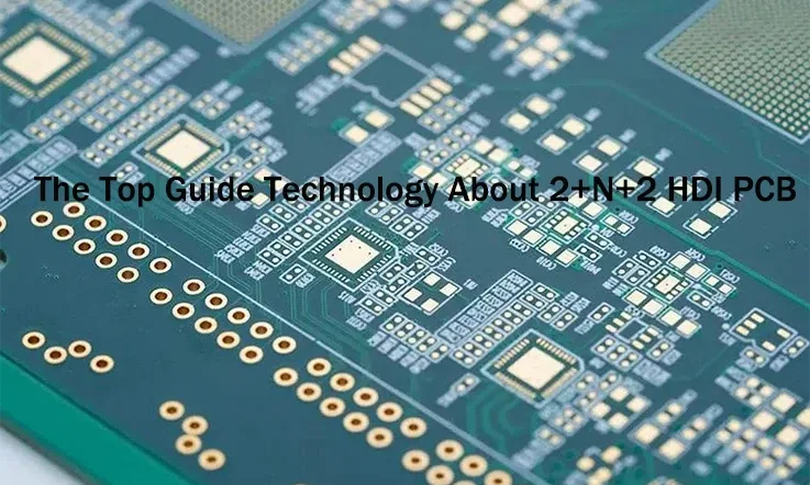
HDI (High-Density Interconnect) PCB have become increasingly popular in the electronics industry due to their ability to accommodate complex designs with high component density. Amongst the diverse catalog of HDI PCB layout, the 2+N+2 arrangement distinguishes itself as both adaptive and proficient. Within this exposition, we delve into the key features, benefits, application, design, and fabrication of 2+N+2 HDI PCB, underscoring their essential role in present-day electronic utilizations.
HDI PCB 2+N+2: Moderate Complex HDI
HDI PCB 2+n+2 is classified as a Type III construction, which employs resin-filled holes, vias, and plated microvias for interconnection purposes. This type follows a sequential buildup denoted as X+n+X.
In the case of a 2+n+2 stack up, a minimum of two, and potentially more, high-density interconnection layers are incorporated on at least one side of the substrate core during the HDI PCB design phase. The substrate core itself can comprise multiple layers and incorporates buried vias to facilitate interconnection. The manufacturing process adheres to established PCB guidelines, and the choice between a flexible or rigid substrate depends on the specific requirements of the intended application.
Microvias are vital in this design, capable of being arranged in both stacked and staggered fashion across various strata. This arrangement enables seamless signal transmission between the layers through these microvias. Due to the small drill diameters and aspect ratio requirements of the vias, the manufacturing process involves a sequential lamination approach. Nonetheless, the utilization of the stacked microvias methodology permits designers to effectively route fine-pitch components using buried or blind vias.
Challenging designs that incorporate copper-filled stacked microvias are commonly implemented in applications demanding high-level signal transmission performance. The HDI PCB 2+n+2 design offers notable advantages in appliances that require increased routing density while maintaining a thin finished thickness of the printed circuit board.
Furthermore, HDI PCB 2+n+2 designs are highly suitable for Ball Grid Arrays (BGAs) due to their ability to accommodate high I/O counts and smaller ball pitch. Consequently, there has been a substantial surge in demand for such designs in the manufacturing of game consoles, cameras, and cell phones.
It is important to note that while the commonly adopted design model for an X+n+X buildup is 2+n+2, structures can extend beyond higher numbers depending on the mechanical and electrical requirements of a given appliance.
Design Considerations for 2+N+2 HDI PCB
When designing a 2+N+2 HDI PCB, there are several important considerations to keep in mind. Here are some key design considerations:
Layer Stack-up:
The arrangement of layer stack-up is paramount within HDI PCB design, shaping the routing density, impedance control and signal integrity. The stack-up requires meticulous planning to house the necessary signal layers, power planes and ground planes, whilst maintaining controlled impedance for high-speed signals.
Routing and Signal Integrity:
HDI PCB frequently play integral roles in high speed and high frequency applications. To uphold signal integrity and diminish signal decay, it is crucial to cultivate precise routing strategies such as regulated impedance routing, differential pairings and length matching.
Via Types and Placement:
HDI PCB utilize various via types, including microvias, buried vias and blind vias, to achieve high routing density. Microvias are small in diameter and provide a high level of density. Careful placement of vias is important to optimize signal paths and minimize crosstalk and interference.
Power and Ground Planes:
Adequate power and ground planes are essential for HDI PCB to provide stable power distribution and minimize noise. The power and ground planes should be properly connected using vias and stitched together to ensure low impedance paths.
Component Placement:
Component placement plays a crucial role in HDI PCB design. Placing high speed components close to each other and minimizing trace lengths can help reduce signal propagation delays and improve signal integrity. Proper thermal management should also be considered to ensure components operate within their temperature limits.
Manufacturing Constraints:
HDI PCB often involve advanced manufacturing techniques, such as laser drilling and sequential lamination. It’s important to consider the manufacturing capabilities and constraints of your chosen PCB manufacturer to ensure the design can be successfully fabricated.
Design for Testability:
Implementing test points and access for test probes is important for efficient testing and debugging of HDI PCB. Designing in test pads and vias for boundary scan testing or other test methodologies can help streamline the manufacturing and testing process.
Thermal Management:
HDI PCB hosting a high granularity of components could generate substantial thermal energy. Implementing appropriate management techniques methodologies, encompassing thermal vias, heat sinks, and thermal pads, is essential to proficiently disperse heat, thereby forestalling component overheating.
These are some of the key considerations when designing a 2+N+2 HDI PCB. It’s important to work closely with experienced PCB designers and manufacturers to ensure your design meets the required performance and reliability standards.
Manufacturing Process of 2+N+2 HDI PCB
Fabricating a 2+N+2 HDI PCB entails a sequence of process that cater to the intricacy and density specifications of the design.
Design and Layout:
The PCB design is created using EDA PCB design software, taking into consideration the specific requirements of the 2+N+2 HDI design, including layer stack up, routing, and component placement. The design is then converted into Gerber files or other manufacturing file formats.
Material Selection:
Material selection remains paramount when manufacturing HDI PCB. High caliber materials boasting superior electrical characteristics, inclusive of specific laminates and prepregs, are chosen in alignment with design prerequisites. Imposing factors influencing material choice might be impedance control, signal integrity and thermal management.
Layer Stack-up and Prepreg Preparation:
The determination of the layer stack-up is carried out in accordance with design parameters, which encompass the count of signal layers, power planes, and ground planes. The prepregs are made ready by trimming them to the appropriate dimensions and adding copper foil on either side.
Drilling:
HDI PCB use microvias, buried vias, and blind vias to achieve high routing density. The drilling process involves using laser drilling machines to create small-diameter holes for the vias. Laser drilling provides high precision and allows for smaller via sizes.
Electroless Copper Deposition:
After drilling, the PCB panels undergo an electroless copper deposition process. This involves depositing a thin layer of copper on the walls of the drilled holes, including the microvias, to create conductive pathways.
Imaging and Plating:
The PCB panels are coated with a photosensitive material called a photoresist. The panel exposure is managed via a photomask crafted from the Gerber files. Upon exposure to UV light, exposed areas of the photoresist react and harden while the unexposed areas maintain their soft texture. After, these panels undergo a chemical process, eliminating the soft regions and preserving the pattern for the internal layers. Subsequently, copper is electroplated onto these exposed portions, shaping the conductive traces.
Lamination and Pressing:
The inner layers are stacked together with the prepregs and copper foil layers, forming a multi layer structure. The stack is then pressed and heated in a lamination press to bond the layers together, forming a solid panel.
Outer Layer Imaging and Plating:
The outer layers of the panel are coated with photoresist, exposed to UV light using the appropriate photomasks, and chemically treated to remove the unexposed areas. The exposed copper areas are then plated to create the outer layer conductive traces.
Solder Mask Application:
A solder mask layer is applied to the entire surface of the PCB, except for the areas where components will be soldered. This layer shields the PCB from factors and helps prevent solder from bridging during assembly.
Surface Finish:
The PCB’s exposed copper surfaces are typically plated with a surface finish to protect them from oxidation and facilitate soldering. Common surface finishes include HASL (Hot Air Solder Leveling), ENIG (Electroless Nickel Immersion Gold), and OSP (Organic Solderability Preservatives).
Routing and Vias:
The PCB panels are routed to separate individual boards, and vias are drilled and plated to provide electrical connections between different layers.
Testing and Inspection:
The finished HDI PCB undergo various testing and inspection processes to ensure they meet the required quality standards. This includes electrical testing, visual inspection, and sometimes automated optical inspection (AOI) or X-ray inspection for more complex designs.
Industries Benefiting from 2+N+2 HDI PCB
2+N+2 HDI PCB technology has significantly penetrated numerous sectors, fostering advancement and delivering an array of benefits. Numerous industries that immensely profit due to the adoption of 2+N+2 HDI PCB include:
Aerospace and Defense:
The aerospace and defense industry demands high-performance, reliable and compact electronic systems. These requirements make 2+N+2 HDI PCB extremely compatible for uses in areas like avionics, radar systems, satellite communication and military-grade hardware. Due to the enhanced routing density and superior signal transmission attributes of 2+N+2 HDI PCB, they are perfectly equipped to comply with the rigid demands typical of this sector.
Telecommunications:
The telecommunications sector depends on communication systems that offer both high speed and high bandwidth. 2+N+2 HDI PCB enable the design and manufacturing of advanced networking equipment, routers, switches, and telecommunications infrastructure components. With their capacity to house fine-pitch components and assure optimal signal transmission, these PCB become indispensable in fulfilling the requirements of contemporary communication networks.
Consumer Electronics:
The consumer electronics industry thrives on compact and feature-rich devices. Like smartphones, tablets, wearables and portable gadgets. 2+N+2 HDI PCB allow for thin and lightweight designs, enabling manufacturers to create sleek and powerful electronic devices. The increased routing density and design flexibility offered by 2+N+2 HDI PCB are crucial in meeting the miniaturization requirements of consumer electronics.
Medical Devices:
The medical industry requires high-performance and reliable electronic systems for various applications, including diagnostic equipment, patient monitoring devices, implantable devices, and imaging systems. 2+N+2 HDI PCB facilitate the integration of complex circuitry and miniaturized components, enabling the development of advanced medical devices with enhanced functionality and precision.
Automotive:
The automotive industry relies on electronics for various applications, including advanced driver assistance systems (ADAS), infotainment systems, engine management, and vehicle connectivity. 2+N+2 HDI PCB play a vital role in enabling the compact and reliable integration of electronics in vehicles, ensuring efficient signal transmission and robust performance in demanding automotive environments.
Industrial and Manufacturing:
Industries such as industrial automation, robotics, and manufacturing equipment benefit from 2+N+2 HDI PCBs’ ability to handle complex control systems and high-speed data processing. These PCB enable the creation of compact and reliable electronic solutions that optimize manufacturing processes and enhance automation capabilities.
These sectors constitute only a portion of the industries that garner advantages from the incorporation of 2+N+2 HDI PCB technology. With continuous evolution and increased performance requirements of electronic systems, the relevance of 2+N+2 HDI PCB will inevitably keep expanding across an extensive array of applications and industrial arenas.
Significance of 2+N+2 HDI PCB stack-up
The importance of the 2+N+2 HDI PCB construction cannot be underestimated within the context of printed circuit board technology. The magnitude of its relevance emanates from numerous critical elements:
Increased Routing Density:
The 2+N+2 HDI PCB structure permits a greater circuit routing density in comparison to conventional PCB layout. This is accomplished through the inclusion of several high density interconnection strata on a minimum of one facet of the substrate core which encourages a more proficient routing procedure for signals and power. The structure is capable of accommodating intricate circuit designs and miniaturized components, thus optimizing functionality.
Improved Signal Transmission:
With the utilization of stacked and staggered microvias technology, the 2+N+2 HDI PCB facilitates unhindered signal transmission between different layers. This ensures reliable and efficient communication between components, especially in high-speed applications where signal integrity is crucial.
Enhanced Design Flexibility:
The 2+N+2 HDI PCB offers greater flexibility in design due to the availability of multiple interconnection layers. Designers can optimize the placement and routing of components, leading to improved functionality and performance of the overall system.
Compatibility with Fine-Pitch Components:
The stacked microvias technology in 2+N+2 HDI PCB enables the use of buried or blind vias, allowing for the routing of fine-pitch components. This capability is particularly advantageous when working with advanced semiconductor devices, such as Ball Grid Arrays, which have high I/O counts and smaller ball pitch.
Thin Profile and Space Savings:
The 2+N+2 HDI PCB structure allows for the creation of thinner and more compact circuit boards. This is especially beneficial in application where space is limited, such as portable electronic devices. The reduced thickness and smaller form factor contribute to lightweight and sleek designs.
Application Versatility:
The 2+N+2 HDI PCB buildup finds extensive application across various industries. It is particularly well-suited for aerospace, military, telecommunications, consumer electronics, and other sectors that demand high-performance and miniaturized electronic solutions.
Leveraging the benefits presented by a 2+N+2 HDI PCB construction, manufacturers can achieve superior functionality, dependability, and miniaturization in their output. This kind of PCB structure stimulates the progression of sophisticated electronic systems capable of satisfying the perpetually escalating requirements of contemporary technology.
How to Choose the Right HDI PCB 2+N+2 Manufacturer?
Experience and Expertise: Look find a manufacturer with a proven track record in producing HDI PCB. They should have experience with complex designs and cutting edge manufacturing techniques.
Technology and Capabilities: Ensure that the manufacturer has the necessary technology and capabilities to meet your specific requirements. This includes their ability to handle high layer counts, fine line and space requirements, microvias and other advanced features.
Quality and Reliability: Check the manufacturer’s quality control processes and certifications. Look for adherence to industry standards such as IPC and ISO. Ask for their quality control procedures, inspection methods, and reliability testing processes.
Production Infrastructure: Consider paying a visit or soliciting information about the infrastructure of the manufacturer. Evaluate their production aptitude, apparatus, and sanitation. A robust facility brimming with contemporary equipment holds the potential of promising superior quality and productivity.
Prototyping and Production Capabilities: Determine if the manufacturer can handle both prototyping and high-volume production. It’s beneficial to work with a company that can support your project from initial design to final production.
Communication and Support: Evaluate the manufacturer’s communication channels and responsiveness. It’s important to have clear and open lines of communication to address any concerns or changes throughout the manufacturing process.
Cost and Lead Time: Consider the manufacturer’s pricing structure and lead times. While cost is a factor, it should not be the sole determining factor. Balancing cost with quality and reliability is crucial to ensure a successful outcome.
Customer Reviews and References: Research the manufacturer’s reputation by checking customer reviews and asking for references. This can provide valuable insights into their past performance and customer satisfaction.
By considering these factors, you can make an informed decision when choosing the right HDI PCB 2+N+2 manufacturer that aligns with your specific requirements and quality expectations.
Why Choose Us?
JarnisTech Provide the Top HDI PCB 2+N+2 Manufacturing Technology
JarnisTech introduces a significant advancement in PCB technology with Our PCB 2+N+2 HDI circuit board, surpassing the capabilities of the previous 1+N+1 HDI PCB board. This cutting-edge high-speed PCB circuit board is meticulously printed and processed using Rogers RO4350B+TUC mixed pressure technology, ensuring exceptional performance.
The 2+N+2 HDI high speed PCB circuit board, a notable addition to JarnisTech’s Type II HDI PCB board series, undergoes rigorous proofing and mass production processes. It is specifically manufactured utilizing Rogers RO4350B+TUC TU872SLK, a top-of-the-line material known for its superior quality and reliability.
This specials types of HDI high speed PCB circuit board is utilized comprehensively in crucial sectors like aerospace and defense where rigorous performance prerequisites hold insurmountable importance. By leveraging JarnisTech’s expertise and the advanced capabilities of the 2+N+2 HDI technology, aerospace and military applications can benefit from enhanced functionality and reliability.
JarnisTech remains committed to pushing the boundaries of PCB manufacturing, delivering state-of-the-art solutions that meet the ever-evolving demands of high speed circuitry. The 2+N+2 HDI high speed PCB circuit board stands as a testament to our dedication to excellence and ability to provide cutting-edge solutions for sophisticated industries.
In Short
We trust that you have gained valuable insights into the various types of HDI PCB structures, particularly the significance of the HDI PCB 2+n+2 buildup. This type of PCB has gained widespread popularity due to the utilization of stacked and staggered microvias technology, enabling enhanced routing capabilities.
Considering the inherent complexities associated with designs featuring increased wire density and layer requirements, we strongly recommend engaging the services of reputable PCB manufacturing experts such as JarnisTech.
As a distinguished producer of printed circuit boards, JarnisTech has carved a significant place for itself as a front-runner within the sector. Our expertise shines in delivering economically viable solutions specifically customized for the electrical appliances industry, while staunchly maintaining high quality benchmarks. Our commitment to state-of-the-art PCB technology and unwavering customer satisfaction sets us apart.
We invite you to visit JarnisTech today and explore our comprehensive range of services. Our team of experts is readily available to provide personalized assistance and promptly provide you with a quote for your custom HDI PCB 2+n+2 designs. Experience the JarnisTech difference and unlock the full potential of your PCB projects.

