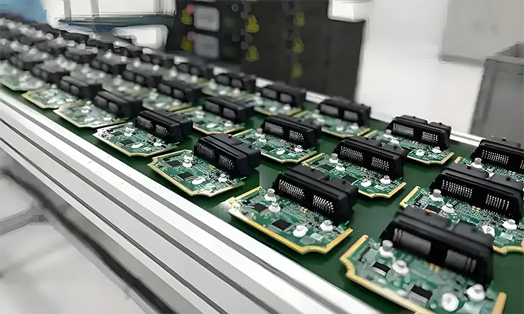
Rogers RO4533 laminates have become a widely adopted PCB base material for RF and microwave circuit applications due to their balanced electrical characteristics and stable mechanical behavior. This guide consolidates a wide range of engineering insights, manufacturing parameters, layout considerations, and performance evaluations related to RO4533-based PCBs. From initial stack-up planning to quality verification and sample requests, each section provides actionable information for engineers, procurement teams, and technical managers working with high-frequency systems. The objective is to support consistent fabrication results while enabling greater clarity in early decision-making across telecom, automotive radar, IoT, and satellite hardware projects.
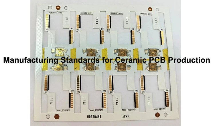
Overview of Rogers RO4533 PCB Technology and RF Applications
When looking for high-performance, low-loss PCBs that meet the demanding needs of high-frequency, microwave, and 5G communication systems, Rogers RO4533 is a solid choice. With its combination of dielectric stability and low loss factors, RO4533 is designed to meet the stringent performance requirements of RF and microwave circuits. To fully appreciate its capabilities, let’s explore what makes RO4533 an excellent option for these types of applications.
What is Rogers RO4533?
An Overview of High-Frequency Laminate
Rogers RO4533 is a high-performance PCB laminate, specially designed for high-frequency applications. This material is part of Rogers’ RF laminate line and is widely used by engineers working on circuits for RF signal transmission and microwave systems. At its core, RO4533 is a hydrocarbon ceramic material that offers the best of both worlds: the low-loss performance of ceramics and the ease of processing typical of organic materials.
What makes Rogers RO4533 stand apart from standard PCB materials is its unique combination of dielectric constant (Dk) stability, low dissipation factor (Df), and low moisture absorption. These qualities help maintain consistent performance across a range of frequencies, temperatures, and environmental conditions. Human’s engineers often choose RO4533 when working with systems where reliable signal integrity and minimal loss are required. For applications like 5G networks, microwave radar systems, and precision medical equipment, RO4533 delivers dependable performance.
| Property | Value |
| Dielectric Constant (Dk) | 3.3 ± 0.08 (at 10 GHz) |
| Dissipation Factor (Df) | 0.0025 (at 10 GHz) |
| Water Absorption | 0.05% |
| Thermal Conductivity | 0.60 W/m·K |
The Dk value influences the impedance of transmission lines, directly affecting signal behavior in high-frequency designs. Materials with low Df tend to support lower signal attenuation, helping maintain signal clarity and limit heat buildup during transmission.
Key Features of RO4533 PCB: Dk, Df, and Signal Loss Control
When working with Rogers RO4533 PCB, it’s necessary to consider the material’s performance characteristics, especially the dielectric constant (Dk) and dissipation factor (Df). These properties influence how effectively signals are transmitted, particularly in RF and microwave systems, where managing energy loss is a primary concern.
Here’s a breakdown of the material’s key attributes:
●Dielectric Constant (Dk): RO4533 has a Dk of 3.3 at 10 GHz, making it a suitable material for impedance-controlled transmission lines. Its stable Dk ensures a consistent signal velocity, which helps achieve optimal performance in high-frequency applications.
●Dissipation Factor (Df): The Df of RO4533 is exceptionally low, around 0.0025 at 10 GHz, which reduces energy loss in the form of heat. This contributes to enhanced signal integrity, ensuring clearer communication for RF and microwave circuits.
●Signal Integrity: With RO4533, the design process becomes simpler when it comes to maintaining signal integrity. When designing 5G infrastructure or military radar systems, the material offers high-performance characteristics that minimize signal degradation and loss.
Incorporating these elements in your design will help maintain consistent signal clarity, reduced crosstalk, and long-term reliability.
Applications in RF, Microwave, and 5G Communications
Rogers RO4533 is a sought-after material in various industries requiring high-frequency, low-loss performance. Its application extends across several fields that rely on superior RF, microwave, and 5G communications.
5G Communication Systems-
With the rapid rollout of 5G networks, the demand for materials that can handle the higher frequencies and greater data rates is greater than ever. Rogers RO4533 is an optimal choice for 5G base stations and small-cell deployments, ensuring signal integrity and performance consistency in these core infrastructures.
Microwave Systems and Radar-
In the field of radar systems, used for military defense or automotive applications, RO4533’s low-loss and stable Dk make it a top contender. When designing for systems operating in the microwave frequency range, such as antenna arrays or radar sensors, the material guarantees precise signal transmission.
Automotive Systems: ADAS and Radar-
As autonomous vehicles become a reality, Advanced Driver Assistance Systems (ADAS) rely on microwave radar to detect objects and obstacles. With its low-loss performance at high frequencies, Rogers RO4533 is an excellent material choice for radar components that operate in the 77 GHz frequency range.
Medical Devices-
In medical imaging systems like MRI and ultrasound equipment, signal clarity is must. Rogers RO4533 helps to ensure precise and clean signal transmission, improving diagnostic quality and making it a reliable choice for high-performance medical PCBs.
Core Material Properties of Rogers RO4533 Laminates
The foundation of any high-frequency printed circuit board (PCB) is its laminate, and when it comes to demanding applications like 5G communication, radar systems, and medical equipment, Rogers RO4533 laminates offer a unique set of properties that help meet the challenges of high-frequency and demanding environments. In this section, we’ll break down the core material properties of Rogers RO4533 that help ensure reliable performance in RF circuits and microwave components.
Dielectric Properties and Consistency of RO4533 Substrates
When dealing with high-frequency signal transmission, dielectric properties determine how well a PCB laminate handles energy without distortion. Rogers RO4533 PCB delivers specific electrical characteristics that help maintain signal clarity and timing in RF environments.
Let’s walk through what makes RO4533 substrate a steady performer:
●Dk (Dielectric Constant): 3.3 ± 0.08 at 10GHz — This value supports impedance control in RF and microwave PCB design. It gives engineers the ability to tune circuits without fighting wild fluctuations.
●Low Df (Dissipation Factor): 0.0025 at 10GHz — Lower energy loss translates into cleaner signal flow, which is exactly what RF engineers look for in high-frequency routing and microwave network layout.
●Uniform dielectric behavior across the board — This means no nasty surprises when signals change frequency. Systems using Rogers RO4533 PCB materials hold performance across applications like 5G antennas, radar front ends, and broadband modules.
●Engineered for consistency — Even during temperature shifts or board bending, the electrical parameters remain steady, so no need to overcompensate in layout tolerances.
So, if you’re building high-speed, high-frequency communication boards — or if your client’s chasing better transmission for phased arrays or RF filters — Rogers RO4533 PCB gets you a well-balanced dielectric response.
Thermal Management Capabilities in Demanding Environments
Temperature shifts are no stranger to RF and microwave applications — especially in the fields of satellite, automotive radar, or outdoor 5G transceivers. That’s where the thermal management behavior of Rogers RO4533 laminate comes into play.
Here’s why Rogers RO4533 stays dependable under pressure:
●Thermal Conductivity: 0.60 W/m·K — This spec helps the material pull heat away from hot components, making it easier to design for power density without frying signal clarity.
●Excellent performance during thermal cycling — Devices using RO4533 PCB materials don’t fall apart after 1,000+ hot/cold cycles. You can count on it for rugged outdoor and aerospace systems.
●High-power RF compatibility — If you’re working on power amplifiers, RO4533 substrates are better suited to disperse thermal buildup evenly, giving circuit life a longer runway.
●Resists expansion under heat — Less board warping means fewer layout alignment issues and better pad integrity for BGAs or fine-pitch connectors.
Z-Axis Expansion, Dimensional Stability, and TCDk
In multilayer RF boards, how a laminate behaves in the Z-axis (thickness direction) can affect solder joint reliability, via connections, and alignment accuracy. Rogers RO4533 PCB materials are engineered with dimensional stability in mind.
Here’s how RO4533 helps in precision designs:
●Low Z-axis CTE (Coefficient of Thermal Expansion) — You won’t get unpredictable swelling or contraction when your circuit heats up. That’s helpful when working with hybrid boards or plated through-holes.
●Dimensional tolerance that behaves — When fabricating RO4533 PCBs, the registration across layers stays tight. This reduces design-time stress for engineers focused on impedance-controlled RF layouts.
●Low TCDk (Thermal Coefficient of Dielectric Constant) — You won’t see wild dielectric changes when your system runs from -40°C to 85°C. That’s one less variable for RF engineers to juggle during simulations or testing.
●Good for mixed-material stackups — RO4533 can be paired with FR-4 or other high-frequency materials in hybrid configurations without bowing, shrinking, or expanding off-spec.
Rogers RO4533 PCB Design Considerations for RF Engineers
When you’re dialing in a high-frequency design, especially in RF and microwave domains, using Rogers RO4533 material opens up some dependable advantages for layout tuning, stack-up, and signal clarity. It behaves predictably across the RF spectrum and offers stable electrical characteristics that make simulation-to-production transitions a bit less hairy. Still, to get the most out of it, you’ll want to design with purpose. The following design methods reflect real-world practices that keep signal flow tight, impedance consistent, and performance locked in across applications like 5G base stations, phased arrays, and radar front-ends.
Impedance Control in High-Frequency PCB Layouts
Impedance control can make or break a high-speed RF design. With Rogers RO4533 PCB, the dielectric constant (Dk) of 3.3 ± 0.08 helps maintain line consistency across broad frequencies — from 1 GHz well into the mmWave bands. This makes it a favorite for microstrip and stripline routing where predictable impedance is needed without excessive recalibration.
Designers often rely on transmission line calculators or 2.5D field solvers when modeling trace widths. For example, achieving a 50Ω impedance with standard RO4533 laminates and 35µm copper typically requires trace widths around 0.30 mm over a 0.20 mm substrate thickness. Throw in matched reference planes and tight routing discipline, and you’ve got yourself a setup that minimizes loss and jitter.
Table: Common Parameters for Impedance Matching on RO4533 PCB
| Parameter | Typical Value | Notes |
| Dielectric Constant (Dk) | 3.3 ± 0.08 | Stable from 1 GHz to 10 GHz |
| Trace Width (50Ω Microstrip) | 0.30 mm | Depends on stack-up |
| Copper Thickness | 35 µm | Standard for RF layers |
| Dielectric Height | 0.20 mm | Affects impedance |
Using such calculated values and consistent routing schemes helps reduce reflection and ensures your layout behaves as expected when you bring it to life. So don’t wing it — model it, simulate it, and lock it in.
Stack-Up Techniques and Simulation for RO4533
PCB stack-up design isn’t just a mechanical concern — it shapes everything from impedance to EMI shielding. When you’re working with Rogers RO4533 PCB fabrication, symmetric stack-ups with well-balanced dielectric and copper layers tend to work better under thermal and mechanical stress.
RO4533 works well alongside RO4450F as prepreg layers, giving you a cohesive dielectric system with predictable bonding behavior. Copper layers should be placed carefully to maintain symmetry, especially when you’re building boards for automotive radar or RF-enabled medical systems.
Table: Sample 6-Layer RO4533 Stack-Up Structure
| Layer Name | Material | Thickness (mm) |
| Top Layer | Copper | 0.035 |
| Prepreg | RO4450F | 0.100 |
| Inner Signal | Copper | 0.035 |
| Core | RO4533 | 0.508 |
| Inner Ground | Copper | 0.035 |
| Prepreg | RO4450F | 0.100 |
| Bottom Layer | Copper | 0.035 |
Simulation software like ADS or HyperLynx can simulate the electrical behavior of this stack-up before fabrication. That’s a smart move when your timelines are tight, and re-spinning boards isn’t on the budget.
Matching Circuit Design and High-Speed Signal Integrity
RO4533 PCB materials perform steadily across temperature and humidity shifts, which is a good thing when you’re building matching networks that can’t afford to drift. In practical terms, we often build L-type or Pi-type networks using trace stubs, SMT components, or etched passive structures — all based on target frequencies and load characteristics.
Differential routing in digital/RF hybrid systems also gets a leg up from RO4533’s uniform dielectric performance. Length matching and spacing are easier to manage when the material doesn’t throw curveballs during lamination or solder reflow. For RF inputs, antenna connections, or chip-to-board interconnects, matching the impedance helps maintain clean transitions with lower VSWR and insertion loss.
Table: Matching Techniques Across RF Signal Types on RO4533
| Signal Type | Matching Strategy | RO4533 Performance Benefit |
| Single-ended | Series resistor | Reduces reflection across DC–3 GHz |
| Differential | AC coupled | Supports trace skew < 0.1 mm |
| Microwave | L-type network | Stable phase over temperature change |
| mmWave | Pi-type network | Low insertion loss at 28 GHz |
So, routing a 2.4 GHz Bluetooth trace or managing data at 28 GHz in a mmWave transceiver both demand consistency in signal behavior. RO4533 provides a stable foundation that supports predictable and repeatable outcomes across such frequency ranges.
Rogers RO4533 Stack-Up Library and Reference Designs
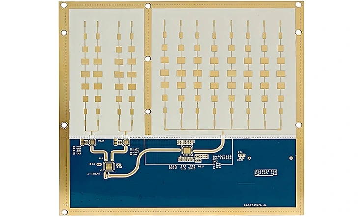
Rogers RO4533 laminate is often selected for multilayer RF PCB configurations due to its well-documented dielectric behavior, mechanical consistency, and compatibility with standard fabrication procedures. When paired with prepreg materials such as RO4450F, the resulting constructions support high-frequency performance without the need for custom processes or exotic handling. Below, we explore practical stack-up arrangements, ready-to-use layout files for simulation, and examples from telecom and IoT applications that follow common industry constraints.
Common Stack-Ups for RO4533 with RO4450F Prepreg
RO4450F prepreg, which shares compatible dielectric and thermal characteristics with RO4533, is often used in multilayer builds. The structure offers a consistent response across GHz-level frequencies, with controlled Z-axis behavior and signal transmission predictability. A typical stack-up might look like this:
| Layer | Material | Thickness (mm) | Use Case |
| Top | Copper | 0.035 | RF trace layer |
| 2 | RO4533 | 0.254 | Primary dielectric |
| 3 | RO4450F Prepreg | 0.101 | Bonding/lamination |
| 4 | Copper | 0.035 | Ground return layer |
This format allows our engineer to maintain consistent impedance and low insertion loss across operational bands such as 2.4 GHz, 5 GHz, and up to mmWave ranges above 20 GHz.
Simulation-Ready Layout Templates
To reduce trial-and-error in design stages, RO4533-based layout libraries are made available in software such as Altium, ADS, or HFSS. These libraries offer:
●Pre-calibrated dielectric constants (Dk = 3.3 @ 10 GHz) and dissipation factors (Df = 0.0025)
●Layer thickness matched to standard prepreg (e.g., RO4450F @ 0.101 mm)
●Cross-sectional impedance control for differential and microstrip configurations
Such templates help ensure continuity between design intent and manufacturing capability, particularly for applications involving filters, couplers, or antenna feedlines where modeling accuracy directly impacts RF system behavior.
Reference Projects in Telecom and IoT
RO4533 constructions appear across a variety of application segments. Below are real-world patterns observed in the field:
●5G Antenna Boards – Deployed in small cell and beamforming modules, typically using 4–6 layer stacks with dual RO4533 cores and single-layer RO4450F bonding.
●Short-Range IoT Nodes – Applied in devices under 1 GHz and Bluetooth/Wi-Fi bands, using thin RO4533 layers for compact design.
●Radar Signal Chains (Automotive) – Found in 24 GHz and 77 GHz modules, using RO4533 with embedded shielding layers for EMI suppression
These examples illustrate use cases where RO4533’s dimensional stability, consistent electrical profile, and thermal compatibility have enabled a range of applications without adding extra processing burdens.
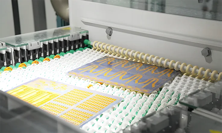
Fabrication Processes for RO4533 PCBs: From Drilling to Final Finish
The fabrication process of RO4533 PCBs demands attention to detail to ensure reliable performance for high-frequency applications. Each stage, from drilling through to surface finishing, contributes to the quality and reliability of the final product. Let’s explore the major processes involved and how they shape the final PCB.
CNC Drilling, Laser Cutouts, and Microvias in RO4533
Drilling is a necessary step in the PCB manufacturing process, especially for high-density designs like those made with RO4533 laminates. Various methods, such as CNC drilling and laser cutouts, are used depending on the design and complexity of the board. Microvias, a popular choice for compact, high-density interconnects (HDI), are especially useful in these designs.
●CNC Drilling: Used to create vias and through-holes, this method is appropriate for larger vias.
●Laser Cutouts: Employed for finer details and smaller vias, offering precision for complex designs.
●Microvias: Used in high-density circuit boards, these small vias are created through laser drilling and support compact layouts by enabling more interconnections within limited space.
Microvias allow for smaller board designs and are particularly useful when space is at a premium. They provide an efficient solution for multi-layer designs, ensuring the necessary interconnects without compromising space.
Copper Plating, Etching, and Lamination Specifics
After drilling, the next step is copper plating, which fills the drilled vias and provides electrical connections between layers. Etching follows to remove excess copper and define the circuit paths. The final stage is lamination, which bonds the layers together to form the finished PCB. This series of processes ensures the strength and conductivity of the finished product.
●Copper Plating: The plating thickness, typically 25 to 35 microns, is determined by the current-carrying requirements.
●Etching: Essential for the fine definition of circuit traces, this process ensures that the board’s conductive paths are accurately defined.
●Lamination: Used to bond the individual layers of the PCB, lamination is done under heat and pressure to avoid delamination or weak spots.
Etching is a meticulous process, as it defines the width of copper traces, and any inaccuracies can affect the board’s performance. The lamination process must be closely controlled to prevent defects such as incomplete bonding or layers that might separate under stress.
Surface Finish Options: ENIG, OSP, Immersion Silver
Once the etching and copper plating are completed, a surface finish is applied to protect the copper and ensure proper soldering. The choice of surface finish depends on the application and specific needs of the PCB. Each surface finish option has its own characteristics and suitability.
●ENIG (Electroless Nickel Immersion Gold): A smooth and solderable surface finish. It’s widely used for fine-pitch components due to its flatness.
●OSP (Organic Solderability Preservative): A more affordable option commonly used for applications with shorter shelf lives and fewer performance demands.
●Immersion Silver: Ideal for high-frequency applications, offering excellent conductivity but requiring careful handling to prevent oxidation.
ENIG is widely chosen for precision applications, as it provides a reliable soldering surface that minimizes the risk of oxidation. OSP, on the other hand, is more suited for lower-end applications where cost considerations outweigh long-term durability. Immersion silver, while offering good conductivity, requires proper storage and handling to avoid tarnishing, which can affect signal integrity.
Electrical and Mechanical Performance of Rogers RO4533 PCBs
High-frequency applications demand consistency—not just in electrical behavior, but also in mechanical durability. Rogers RO4533 PCBs are well-suited for this challenge, thanks to their engineered laminate structure and predictable material behavior under RF and thermal stress. Let’s explore the specific performance characteristics that matter when working with Rogers RO4533 PCB materials in advanced PCB fabrication environments.
Electrical Stability Over Wide Frequency Ranges
Maintaining dielectric stability across GHz-level frequencies can directly affect signal transmission, impedance matching, and energy efficiency. Rogers RO4533 was developed to address these challenges head-on, offering consistent RF performance.
●Dielectric Constant (Dk): approximately 3.33 @ 10 GHz—minimizing phase distortion across broadband designs.
●Dissipation Factor (Df): about 0.0025—reduces insertion loss in microwave PCBs and 5G circuits.
●Stable electrical behavior from MHz through 40 GHz—suitable for radar, satellite, and phased-array systems.
●Low moisture uptake (~0.02%)—ensures dielectric consistency under humidity and condensation exposure.
●Consistent performance when paired with hybrid stack-ups using other Rogers PCB materials like RO4350B.
Mechanical Robustness, Vibration Resistance, and Reliability
Applications involving heat cycling, vibration, or physical flexing benefit from materials that don’t shift or delaminate over time. Rogers RO4533 meets those expectations through thermal and mechanical consistency.
●Coefficient of Thermal Expansion (CTE): ~13 ppm/°C (X), ~11 ppm/°C (Y)—reduces expansion mismatch with copper.
●Flexural strength enables stability in high-speed backplanes and aerospace RF boards.
●Withstands mechanical stress in automotive radar and RF amplifier environments.
●Excellent via wall integrity after thermal stress testing—minimizes failure risk during RO4533 PCB fabrication.
●Supports rigid or semi-flex configurations, depending on layout needs and laminate thickness.
Bonding Strength with Copper Foils and Inner Layers
Layer adhesion determines the structural performance of multilayer RF boards. Rogers RO4533 is engineered for high interlaminar adhesion with copper, enabling secure stack-up bonding during lamination.
●Peel Strength: typically 6.9 lb/in (1.2 N/mm) with standard electrodeposited copper foil.
●Lamination compatibility with prepreg and other Rogers PCB materials in hybrid builds.
●High bond retention after thermal shock and reliability testing—reduces risk of copper lifting or delamination.
●Surface texture promotes clean copper etching and predictable impedance during RO4533 PCB design.
●Compatible with ENIG, OSP, and Immersion Silver surface finishes used in high-reliability RF circuit designs.
Reliability and Testing of Rogers RO4533 Circuits
Rogers RO4533 substrates are frequently used in RF and microwave systems where consistent, predictable behavior under variable environmental and operational stressors is required. As part of standard manufacturing quality assurance, these materials undergo multiple validation stages, from thermal durability checks to electrical verification, to help ensure they’re ready for field deployment.
Thermal Cycling and Environmental Chamber Tests
RO4533-based boards are exposed to a variety of environmental trials that simulate real-world conditions. These include rapid temperature swings and humidity changes designed to observe mechanical cohesion and laminate behavior.
●Thermal cycling from -40°C to +125°C over hundreds or thousands of cycles.
●Thermal shock testing between extreme temperature extremes.
●CTE matching checks between copper and substrate layers to limit stress buildup.
Thermal Stress Testing Overview-
| Test Type | Temperature Range (°C) | Cycle Count | Pass Criteria |
| Thermal Cycling | -40 to +125 | 1000 cycles | No delamination |
| Thermal Shock | -55 to +125 | 500 cycles | No via cracks |
| CTE Compatibility | -40 to +150 | 1000 cycles | No blistering |
These routines are commonly used in automotive radar PCB boards, aerospace navigation systems, and other high-reliability RF modules.
Electrical Testing (Flying Probe, AOI, X-Ray)
Once fabrication is complete, RO4533 PCBs are evaluated through multiple non-destructive electrical and optical inspection methods. Each type of test identifies specific defect types that could affect long-term performance.
●Flying probe testers scan for shorts, opens, and resistance anomalies.
●AOI systems check for trace integrity, spacing consistency, and solder mask accuracy.
●X-ray imaging is applied for BGA inspection and via structure confirmation.
Inspection Method Comparison-
| Test Method | Purpose | Stage Applied |
| Flying Probe | Detects opens, shorts, resistance deviations | Final Test |
| AOI | Checks trace width, spacing, mask alignment | Panel Fabrication |
| X-Ray | Confirms BGA via fill, inner-layer alignment | Mid & Final Test |
These inspection tools provide strong feedback on whether a board meets build-to-print criteria.
Impedance and Loss Verification in QA Stages
High-frequency circuits demand tight control over signal transmission characteristics. Rogers RO4533 PCBs are checked using specialized instruments that focus on impedance and RF performance metrics.
●TDR (Time Domain Reflectometry) validates impedance uniformity across controlled traces.
●VNA (Vector Network Analyzer) measures insertion and return loss.
●S-parameter data is used to assess how signals propagate through the structure.
Electrical Performance Evaluation-
| Measurement | Tool Used | Typical Frequency Range (GHz) | Acceptance Range |
| TDR | TDR Tester | 1 to 10 | ±5% impedance |
| Insertion Loss | VNA | 1 to 40 | <0.5 dB/in |
| S11 | VNA | 1 to 40 | <-15 dB |
| S21 | VNA | 1 to 40 | >-10 dB |
These assessments help PCB manufacturers align RO4533 PCBs with the needs of millimeter-wave antennas, phased arrays, and satellite radio modules.
RO4533 PCB vs RO4003C PCB vs RO4350B PCB
In RF and microwave hardware development, performance stability, cost control, and delivery timing shape real-world project decisions. While RO4533, RO4003C, and RO4350B are all known laminate options from Rogers Corporation, how these PCBs behave across manufacturing and field deployments can draw a clearer line for practical selection. Below is a direct comparison grounded in fabrication outcomes and system use—not just materials on paper.
Electrical Properties and Application Suitability
For RF circuits ranging from 1 GHz to above 20 GHz, human typically track insertion loss, impedance behavior, and how well a board holds its signal path over time. Here’s how the three PCBs perform in field-oriented tests:
●RO4533 often supports antenna modules in mid-band 5G and radar front ends, where multilayer stack-ups are required. Its performance holds steady in phased array designs and base station deployments.
●RO4003C tends to match well with narrowband wireless and basic RF switching circuits. It finds use in short-range communication devices, though its Dk drift may limit it for higher-layer multilayer layouts.
●RO4350B remains a suitable for base station backhaul or low-loss RF filters, handling consistent GHz behavior in mmWave designs without intensive impedance tuning.
We should weigh the test environment (e.g., temperature cycles, humidity, or vibration) when selecting among the three—not all of them behave the same when pushed under stress.
Manufacturing Compatibility and Cost Differences
From a factory point of view, RO4003C leads in availability and handling ease. Its similarity to FR4 in process compatibility makes it widely accepted by fabs across Asia and North America. Here’s a closer look:
●RO4003C can often run on FR4 lines with adjusted lamination pressure, offering lower pricing due to common stock and tooling.
●RO4533 calls for tighter process control—particularly during lamination and via drilling—due to its composite filler structure. This may affect shop yield if unadjusted.
●RO4350B sits between the two: more stable in plated-through hole steps than RO4533, while more thermally demanding than RO4003C.
Lead time can swing depending on the region. RO4003C may ship faster due to global warehousing, while RO4533 sometimes requires a few extra days for sourcing unless pre-booked.
Long-Term Reliability for RF and High-Speed Systems
Durability under field conditions defines system-level trust. For hardware shipped into automotive radar, remote base stations, or satellite subsystems, boards need to resist signal shift, warpage, and delamination over time.
●RO4533 scores well in environments with thermal cycling and vibration exposure. Its low Z-axis expansion supports good via reliability across multi-pass soldering.
●RO4003C, being more rigid and less resistant to moisture absorption, may require thicker soldermask or surface finish adjustments in outdoor use cases.
●RO4350B has shown long-term stability in exposed telecom gear, especially where wide temperature swings occur (e.g., outdoor cabinets).
As a takeaway, RO4533 leans toward projects with mixed-signal, multilayer complexity. RO4003C offers a better for cost-sensitive, mid-frequency designs. RO4350B stays in the mix for mid-power RF chains that demand consistent losses without complex tuning.
Engineering Custom Rogers RO4533 PCB Solutions
Creating customized solutions with Rogers RO4533 requires attention to process compatibility, stack-up logic, and cooperative execution between fabrication and RF layout teams. The material’s processing traits allow it to integrate well into builds that must meet exacting RF demands without introducing atypical production steps. This section explores three core areas: manufacturability in complex stackups, handling multilayer builds, and coordinating between layout and process engineers.
DFM for Complex RO4533 Stackups
Design for Manufacturability (DFM) underpins successful outcomes with RO4533, particularly for stackups involving mixed laminates or tight tolerances. Instead of adjusting fabrication to fit the board, the build plan should be tuned to work within equipment capabilities.
●Symmetrical Stack Arrangement – Prevents bowing or twisting during lamination.
●Tg and CTE Matching – Keeps layers stable across thermal cycles by aligning thermal properties.
●Prepreg Flow Control – Maintains dielectric thickness uniformity and prevents voiding.
A well-executed stack plan reduces the likelihood of rework and delays, especially in volume builds.
High Layer-Count PCB for RF Routing
RF circuits used in compact systems frequently require stackups with more than 8 or even 12 layers. RO4533 maintains stable performance during lamination, allowing for such configurations. However, careful attention to layer order and thermal behavior is necessary to prevent unwanted coupling and signal attenuation.
●Embedded Ground and Return Paths – Helps maintain consistent reference across routing layers.
●Via Strategy – Blind, buried, or microvia options must be selected based on access and density.
●Copper Balancing – Controls Z-axis expansion and press-out variation during lamination.
This setup has been widely used in phased-array antenna modules and automotive radar where routing space is at a premium.
Collaboration with RF Design Engineers
Consistent communication between fabrication teams and RF layout engineers eliminates blind spots that could otherwise lead to yield loss or out-of-spec performance. This coordination typically starts early in the layout stage.
●Stackup Signoff Protocol – Confirms thickness, impedance values, and material sequencing.
●Tuning Windows and Guard Structures – Integrated to avoid late-stage layout revisions.
●DFX Reviews (Design for Fabrication, Test, Assembly) – Clarifies what tolerances can and can’t be held.
This approach has been proven in mmWave systems, satellite modules, and wireless backhaul projects where signal loss budgets leave no room for guesswork.
Contact Our Expert Team for Rogers RO4533 PCB Manufacturing – JarnisTech
For projects requiring steady high-frequency electrical performance and consistent fabrication, Rogers RO4533-based circuits offer a well-aligned material foundation. At JarnisTech, we support your process from early schematic consideration to final production evaluation. Our approach focuses on maintaining fabrication consistency and electrical behavior while providing flexibility for specific layout strategies.
Engineering Support for RF Circuit Optimization
Our team works closely with layout personnel to ensure the circuit is well-prepared for manufacturing. We assess impedance targets, via density, stack-up consistency, and transition zones. This step reduces the likelihood of multiple prototyping rounds and improves readiness for downstream processing.
Common evaluation points include:
| Parameter | Typical RO4533 Value | Performance Note |
| Dielectric Constant (Dk) | 3.3 ± 0.08 | Consistent across high frequencies |
| Dissipation Factor (Df) | ~0.0025 | Maintains signal integrity at GHz speeds |
| Z-Axis CTE | ~46 ppm/°C | Supports plated-through-hole stability |
| Thickness Availability | 0.254mm to 0.813mm | Enables various stack-up arrangements |
For improved predictability, we recommend sending your layout files early for a full technical review.
Submit Gerber Files for Quote and DFM Review
We offer design checks alongside quoting to help confirm manufacturability. Once you submit Gerber data and supporting files (drill files, BOM, mechanical drawing), we review trace geometry, drill alignment, copper balance, and reference plane allocation. The outcome is a fabrication plan aligned with actual production capabilities.
Review focus areas:
| Review Focus | Example Issues Identified |
| Trace and Gap Dimensions | Incompatibility with copper weight or stack-up |
| Pad-to-Hole Ratio | Margins below required tolerances |
| Mask Opening Alignment | Potential for bridging or exposure mismatch |
| Layer Stack Arrangement | Overlapping signal layers without reference planes |
| Profile and Outline | Dimensions outside milling constraints |
Complete quotes and DFM evaluations are typically provided within two business days.
Request Sample or Small-Batch Rogers PCB
For validation or pre-production purposes, we offer smaller quantity builds using the same material and fabrication processes as used in full-scale production. These small runs allow early-stage assessment without full-volume commitment.
Trial run options:
| Specification | Available Values |
| Quantity Range | 5 to 100 boards |
| Lead Time | 3–5 business days (standard turnaround) |
| Material Thickness | 0.254mm, 0.508mm, 0.813mm |
| Surface Finish Options | ENIG, immersion silver, bare copper |
| Copper Weight | 0.5 oz, 1 oz, 2 oz |
Submit your request for a sample run to validate electrical and mechanical performance before full rollout.
Rogers RO4533 PCB(FAQ)
1.What is the typical glass transition temperature (Tg) of RO4533 laminate?
RO4533 does not have a defined Tg like standard FR4; it behaves as a thermoset resin with consistent properties across a broad temperature range.
2.Can RO4533 be used in mixed dielectric stackups?
Yes, RO4533 is often paired with materials like RO4450F prepreg or RO4003C cores to meet specific RF and mechanical demands.
3.Does RO4533 support embedded passive components?
It allows embedded resistors and capacitors, but this should be validated through prototyping due to process variations.
4.What is the moisture absorption rate of RO4533?
RO4533 typically absorbs less than 0.3% moisture, which supports consistent RF performance in humid environments.
5.Is RO4533 suitable for mmWave frequency ranges?
It can be applied up to 40 GHz depending on layer configuration and design layout precision.
6.How does RO4533 handle thermal expansion?
Its z-axis CTE is around 32 ppm/°C, offering relatively balanced expansion behavior with copper layers.
Our services
Rogers PCB Laminates & Series