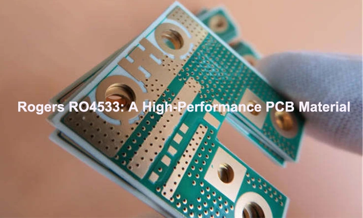
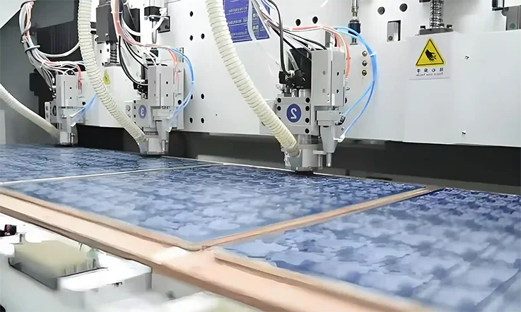
In the world of printed circuit board (PCB) manufacturing, nickel plating is far more than just a protective layer—it directly impacts electrical performance, mechanical durability, and long-term reliability. Whether used in ENIG (Electroless Nickel Immersion Gold), ENEPIG (Electroless Nickel Electroless Palladium Immersion Gold), or standalone applications, the plating process demands tight control over thickness, bath chemistry, and process parameters to avoid defects like black pad formation, oxidation, or adhesion failures.
From high-speed data transmission in AI computing and 5G networks to high-temperature stability in aerospace and automotive electronics, nickel plating continues to evolve to meet the growing demands of modern PCB applications. This guide dives deep into nickel plating PCB surface finish processes, quality control techniques, and defect mitigation strategies, providing real-world insights for PCB manufacturers, design engineers, and assembly specialists. So, if you’re looking to optimize plating efficiency, improve yield, or ensure compliance with industry standards like IPC-6012 and MIL-PRF-31032, you’ll find practical solutions and best practices here.
So, buckle up—it’s time to explore how nickel plating can take your PCB designs to the next level.
Understanding Nickel Plating PCB Surface Finish
Nickel plating plays an indispensable role in PCB manufacturing, serving as both a protective layer and an electrical performance enhancer. So, if you’re designing RF circuits, high-speed digital boards, or aerospace-grade electronics, understanding nickel plating surface finishes can lead to better performance, enhanced durability, and reliable signal transmission.
This section covers the fundamentals of Nickel Plating PCB Surface Finish, diving into its impact on circuit performance, suitability for different applications, and how it compares with alternative finishes.
Nickel Plating in PCB Surface Finishing: What You Need to Know?
Nickel plating involves applying a protective and functional layer over PCB copper traces. This process is commonly used in multi-layer PCBs, RF circuit designs, and high-speed digital boards, where maintaining consistent electrical properties is a priority.
Nickel’s Contribution to Conductivity and Oxidation Resistance-
Nickel is frequently used as an intermediate layer between copper and gold in surface finishes such as ENIG (Electroless Nickel Immersion Gold) and ENEPIG (Electroless Nickel Electroless Palladium Immersion Gold). This provides:
| Nickel Property | Impact on PCB Performance |
| High Hardness | Protects contact areas from wear and tear |
| Corrosion Resistance | Prevents oxidation, ensuring stable conductivity |
| Diffusion Barrier | Prevents copper migration, maintaining signal integrity |
| Solderability | Enhances bonding reliability for SMT and BGA assembly |
Therefore, nickel plating is commonly used in high-frequency PCBs to maintain low-loss signal transmission.
Nickel as a Diffusion Barrier: Why It’s a Go-To Choice in PCB Manufacturing-
Without a diffusion barrier, copper atoms migrate into adjacent metal layers over time. This can result in:
●Weakened solder joints, making assemblies prone to mechanical stress.
●Signal degradation, which affects high-speed data transmission.
●Surface oxidation, reducing contact reliability in connectors and plated through-holes (PTHs).
Industries such as automotive, aerospace, and telecommunications depend on nickel plating to ensure long-term stability under extreme conditions.
How Nickel Plating Stacks Up Against Other PCB Surface Finishes-
Nickel plating isn’t the only game in town when it comes to PCB surface treatments. Here’s how it compares to other popular options:
| Surface Finish | Advantages | Best Applications |
| ENIG (Electroless Nickel Immersion Gold) | Flat surface, good solderability, oxidation-resistant | HDI PCBs, BGA components, high-density circuits |
| ENEPIG (Electroless Nickel Electroless Palladium Immersion Gold) | Better wire bonding capability, prevents “black pad” defects | Aerospace, medical electronics, automotive PCBs |
| HASL (Hot Air Solder Leveling) | Cost-effective, easy to process | Consumer electronics, general-purpose PCBs |
| OSP (Organic Solderability Preservative) | Low cost, environmentally friendly | Budget-oriented PCB applications |
ENIG and ENEPIG remain the most widely used nickel-based surface finishes, while electroplated nickel is preferred for edge connectors and high-wear applications.
Why Nickel Plating PCB Surface Finish Is Preferred for High-Performance Applications?
Nickel plating provides more than just corrosion resistance—it contributes to assembly efficiency, long-term durability, and signal stability, making it a dependable option for high-reliability designs.
Soldering Performance, Durability, and Mechanical Strength-
Nickel-plated PCBs can withstand multiple soldering cycles, making them suitable for reworkable designs and high-reliability applications. This results in:
●Stronger solder joints, reducing failures in high-vibration environments.
●Longer PCB lifespan, even in harsh industrial conditions.
●Reliable contact areas, ideal for gold fingers, edge connectors, and switch contacts.
How Nickel Plating Supports High-Frequency Signal Performance-
For RF, microwave, and high-speed digital circuits, maintaining low signal loss is a priority. Nickel plating helps by:
●Reducing signal attenuation at GHz frequencies.
●Offering consistent plating thickness, minimizing impedance mismatches.
●Improving reliability in RF connectors and microwave substrates.
For technologies like 5G networks, IoT, and radar systems, nickel-plated surfaces help preserve signal clarity and minimize interference.
Heat Resistance for Automotive and Aerospace Applications-
Nickel plating is widely used in engine control units, avionics, and industrial automation systems. It provides:
●Thermal stability up to 500°C, preventing oxidation-related failures.
●Efficient heat dissipation, reducing stress on power electronics.
●Resistance to metal fatigue, ensuring longevity in harsh environments.
For power modules, battery management systems, and space-grade electronics, nickel plating is an industry standard for reliable long-term performance.
Nickel Plating Methods: Choosing the Right Process for Your PCB Design
Different nickel plating techniques exist, each with its own strengths. The best method depends on board complexity, cost considerations, and end-use applications.
Electroplated Nickel vs. Electroless Nickel: What’s the Difference?
The choice between electroplated and electroless nickel depends on where and how the PCB will be used.
| Nickel Plating Type | Deposition Process | Best For |
| Electroplated Nickel | Uses external current; results in harder coatings | Gold fingers, edge connectors, wear-resistant areas |
| Electroless Nickel | Auto-catalytic process; ensures uniform thickness | ENIG, ENEPIG, high-density PCB layers |
For HDI and flexible circuits, electroless nickel ensures even coverage, while electroplated nickel offers better mechanical strength for wear-prone surfaces.
ENIG and ENEPIG: Why They Dominate the Industry-
ENIG and ENEPIG are go-to choices for many electronics industries, thanks to:
●Flat surfaces, making them ideal for fine-pitch components.
●Reliable oxidation resistance, extending PCB shelf life.
●Consistent solderability, reducing defects in mass production.
Tailoring Nickel Plating to HDI, Flexible, and High-Speed PCBs-
Selecting the right plating method ensures that the final PCB meets design expectations without compromising manufacturing efficiency.
Nickel Plating PCB Surface Finish: Advanced Manufacturing Processes and Quality Control
Producing a high-reliability nickel-plated PCB surface finish isn’t just about dipping a board into a chemical bath and hoping for the best. Precision plating requires tight process control, meticulous quality assurance, and a deep understanding of electrochemical and chemical deposition principles.
This section takes a deep dive into electroplated nickel, electroless nickel, and hybrid nickel plating finishes, covering the technical know-how needed to maximize performance, eliminate defects, and meet stringent industry standards.
Electroplated Nickel PCB Surface Finish: Process Control and Optimization
Electroplating is widely used in PCB manufacturing due to its ability to deposit precise layers of nickel onto conductive surfaces, ensuring durability and consistent electrical performance.
Electrochemical Deposition: Bath Chemistry, Temperature, and Current Density-
Electroplated nickel relies on a controlled electrochemical reaction to deposit a uniform layer of metal onto PCB contact pads, edge connectors, and solderable surfaces. The plating bath composition and operating parameters directly affect deposit quality.
| Parameter | Typical Range | Impact on Plating Quality |
| Nickel Sulfate (NiSO₄) | 200-300 g/L | Affects deposition rate and coating structure |
| Boric Acid (H₃BO₃) | 30-50 g/L | Stabilizes pH and prevents rough deposits |
| pH Level | 3.5-4.5 | Controls plating uniformity and adhesion |
| Temperature | 45-60°C | Affects plating speed and stress level |
| Current Density | 2-5 A/dm² | Higher current boosts deposition but may cause roughness |
Pro Tip: Maintaining consistent agitation and solution filtration prevents particle contamination, leading to a smoother, defect-free nickel layer.
Process Control: Thickness Uniformity and Plating Rate Optimization-
Inconsistent plating thickness can wreak havoc on PCB reliability, leading to variable impedance in high-frequency circuits and poor solder joint integrity.
●Pulse plating techniques help control grain structure, ensuring a dense, uniform deposit.
●Automated bath monitoring prevents chemical imbalances that lead to brittle plating layers.
●Current distribution analysis ensures even deposition on fine-pitch PCB designs.
A well-controlled nickel electroplating process results in a smooth, solderable, and corrosion-resistant finish that meets IPC standards.
Common Defects: Poor Adhesion, Roughness, and Contamination Issues-
Even small deviations in process parameters can introduce serious quality issues:
| Defect | Possible Causes | Preventive Measures |
| Poor Adhesion | Improper surface cleaning, oxidation, or low current density | Enhanced pre-cleaning and activation steps |
| Rough Deposits | Contaminated bath, excessive current, or poor filtration | Frequent bath maintenance and optimized current control |
| Internal Stress | Excessive plating thickness or improper pH balance | Controlled deposition rate and stress-relief annealing |
Avoiding these pitfalls requires a well-calibrated plating process and robust quality control measures.
Electroless Nickel PCB Surface Finish: High-Reliability Applications
Unlike electroplating, electroless nickel plating (ENP) deposits a uniform layer of nickel without using an external power source, making it’s suitable for complex PCB geometries and fine-pitch components.
Autocatalytic Deposition: Chemical Reactions and Process Control-
Electroless nickel plating relies on a self-sustaining chemical reaction where nickel ions are reduced onto the PCB surface.
●Hypophosphite (H₂PO₂⁻) serves as the reducing agent, controlling deposition speed.
●The absence of electrical current results in uniform plating thickness, even in vias and intricate surface features.
●pH stabilization prevents bath decomposition and ensures consistent deposit structure.
Phosphorus Content in Nickel: Low, Medium, and High Phosphorus Plating-
The phosphorus level in electroless nickel coatings dictates the final material properties:
| Phosphorus Level | Deposit Properties | Best Applications |
| Low (2-5%) | Hard, wear-resistant, slightly magnetic | Edge connectors, gold fingers |
| Medium (6-9%) | Balanced corrosion resistance & hardness | General-purpose PCB coatings |
| High (10-13%) | Superior corrosion resistance, non-magnetic | Medical, aerospace, and RF PCBs |
Selecting the right phosphorus content ensures that PCB finishes meet durability and environmental demands.
Preventing Oxidation, Black Pad Defects, and Surface Contamination-
Common electroless nickel plating issues include:
●Black pad formation, caused by excessive phosphorus segregation.
●Surface contamination, leading to soldering failures in BGA and QFN components.
●Oxidation problems, affecting PCB lifespan in harsh operating environments.
Proactive bath maintenance, pH monitoring, and contamination control can eliminate these defects.
Hybrid Nickel Plating Finishes for High-Performance PCBs
For next-gen electronics, hybrid finishes like ENIG and ENEPIG provide superior protection and performance.
ENIG vs. ENEPIG: Gold and Palladium Protection for Solderability and Wire Bonding-
| Finish Type | Composition | Advantages |
| ENIG | Electroless Nickel + Immersion Gold | Smooth surface, excellent solderability |
| ENEPIG | Electroless Nickel + Palladium + Immersion Gold | Better gold wire bonding, prevents “black pad” |
ENEPIG is the go-to choice for advanced PCB designs, especially in AI computing and automotive applications.
Advanced Nickel-Alloy Coatings for Automotive, Medical, and AI Computing-
Specialized nickel-phosphorus alloys provide:
●Higher thermal stability, perfect for engine control units and aerospace circuits.
●Improved oxidation resistance, it’s good for medical implants.
●Reduced signal loss, making them suitable for high-speed AI-driven computing.
SEM & Cross-Sectional Analysis for Process Validation-
To ensure quality and compliance, SEM (Scanning Electron Microscopy) and cross-sectional analysis help:
●Detect coating defects before they impact PCB performance.
●Measure plating thickness and grain structure.
●Verify adhesion quality under different soldering conditions.
How Thick is Nickel Plating in PCB Manufacturing?
Nickel plating thickness in PCB manufacturing is carefully selected based on corrosion protection, solderability, and electrical performance needs. A well-controlled layer of nickel ensures long-term reliability, oxidation resistance, and stable interconnections in electronic assemblies. The required thickness varies depending on the application, operating environment, and final surface finish requirements.
For most electronic circuits, nickel plating typically ranges between 2 to 6 micrometers (μm). This range provides an effective diffusion barrier between copper and gold while maintaining solderability and electrical conductivity. However, for high-reliability applications, such as automotive control systems, aerospace electronics, and semiconductor packaging, the nickel layer is often increased to 6 to 12 μm or more to withstand harsh environments, mechanical stress, and thermal cycling.
While a thin nickel deposit improves high-frequency performance by reducing insertion loss, an excessively thick layer may introduce electrical resistance that affects RF and high-speed digital signals. We must strike a balance between durability, conductivity, and plating efficiency when specifying nickel thickness.
Nickel Thickness and Diffusion Barrier Performance
One of the primary reasons for applying nickel plating on a PCB is to act as a barrier layer that prevents copper diffusion into the final surface finish, such as gold or palladium. If the nickel layer is too thin, copper atoms can migrate over time, leading to contact resistance issues and surface degradation.
●2-3 μm nickel layer offers basic diffusion control but may be insufficient for applications exposed to high temperatures or prolonged aging.
●4-6 μm layer is commonly used in ENIG (Electroless Nickel Immersion Gold) finishes, providing good oxidation resistance and stable solderability.
●6-12 μm deposit is applied in main applications where higher mechanical strength and corrosion resistance are required.
When dealing with wire bonding applications or connectors with repeated mating cycles, a thicker nickel layer enhances surface durability and prevents gold embrittlement over time.
Impact of Nickel Thickness on Solderability and Joint Strength
The composition and thickness of nickel plating significantly influence solder joint formation and long-term reliability. A properly plated nickel layer allows uniform solder wetting and strong intermetallic bonding with the solder alloy.
●Thinner nickel deposits (2-4 μm) generally improve solder wetting but may compromise durability in harsh environments.
●A mid-range deposit (4-6 μm) is widely used in RoHS-compliant lead-free soldering to prevent black pad defects and ensure consistent joint integrity.
●Thicker layers (8-12 μm) enhance mechanical strength, particularly in automotive power electronics and aerospace systems, where vibration and temperature fluctuations are frequent.
However, excessive nickel thickness can lead to brittle intermetallic compounds, making it necessary to fine-tune the plating process based on specific soldering conditions and operational stress factors.
Nickel Plating and High-Frequency Signal Performance
For 5G networks, AI processors, and high-speed computing, signal integrity is a major concern. Nickel, having higher electrical resistance than copper, can introduce signal loss and increased impedance if applied in excessive thickness.
●At frequencies below 1 GHz, standard nickel plating (3-6 μm) has minimal impact on signal attenuation.
●For RF circuits operating at 10 GHz or higher, we prefer a thinner nickel deposit (2-4 μm) to minimize insertion loss.
●High-speed digital PCBs require careful thickness control to prevent signal reflections and impedance mismatches.
By optimizing nickel thickness, we can achieve a balance between diffusion control and minimal signal degradation, ensuring high-speed performance without compromising reliability.
Process Control to Maintain Consistent Nickel Thickness
Achieving uniform nickel deposition across the PCB surface requires precise bath chemistry, plating time, and current density management. Two primary plating methods are used:
●Electroplated Nickel: Thickness is adjusted by controlling plating time and current flow. This method is preferred when higher mechanical durability is needed.
●Electroless Nickel: Achieves even coverage without the need for external current, making it suitable for fine-pitch components and HDI (High-Density Interconnect) boards.
Many PCB Manufacturers use X-ray fluorescence (XRF), scanning electron microscopy (SEM), and cross-sectional analysis to monitor plating thickness and ensure it meets performance and reliability standards.
Selecting the Right Nickel Thickness for PCB Applications
Choosing the appropriate nickel thickness depends on operational requirements, surface finish type, and reliability expectations.
●For general-purpose electronics, a 2-6 μm deposit provides a well-balanced mix of solderability and corrosion resistance.
●For harsh environments, such as automotive and aerospace applications, a 6-12 μm layer enhances durability against oxidation and wear.
●For RF and high-speed circuits, a 3-5 μm nickel layer is optimized to reduce signal loss while maintaining intermetallic stability.
How Nickel Plating PCB Surface Finish Impacts Electrical & Mechanical Performance?
When designing high-performance PCBs, the surface finish directly affects electrical conductivity, corrosion resistance, and soldering reliability. Nickel plating has been a trusted choice for decades, providing a strong shield against oxidation while enhancing long-term durability.
But here’s the catch—not all nickel plating processes are created equal.
●How does nickel thickness affect high-frequency signals?
●What’s the best way to reduce insertion loss in 5G and AI-driven applications?
●How can nickel plating protect PCBs in extreme environments?
Let’s dig into the science behind nickel plating PCB surface finish, breaking down why human rely on it and how to optimize the process for peak performance.
Nickel Plating’s Effect on Conductivity and Signal Integrity
Nickel is widely used in PCB surface finishing, but its electrical properties come with trade-offs. While it provides excellent protection, excessive thickness can affect conductivity, especially in high-frequency designs.
Impact of Nickel Layer Thickness on High-Frequency Signal Transmission-
Nickel has higher electrical resistivity (6.99 μΩ·cm) compared to copper (1.68 μΩ·cm), meaning a thicker nickel layer can create resistance and signal degradation.
| Nickel Thickness (µm) | Effect on Signal Transmission |
| < 2 µm | Insufficient barrier, risk of diffusion |
| 3-6 µm | Balanced conductivity and diffusion control |
| > 7 µm | Increased resistance, possible signal degradation |
For instance, in 5G RF modules, where every decibel of loss matters, keeping nickel within the 3-5 µm range helps maintain low insertion loss.
Managing Skin Effect, Impedance Matching, and RF Performance-
At frequencies above 1 GHz, the skin effect forces current to travel along the outermost layer of the conductor, increasing resistance.
●Thick nickel plating amplifies resistive losses, impacting RF/microwave performance.
●Using ENEPIG (Electroless Nickel Electroless Palladium Immersion Gold) can reduce signal degradation, as palladium provides a smoother transition layer.
●Precise impedance matching is achieved by controlling plating thickness, ensuring stable transmission line performance.
Reducing Insertion Loss in 5G, AI Computing, and HPC Applications-
High-speed computing and AI-driven hardware demand low-loss PCB materials. Nickel plating, when overdone, can be a silent culprit in signal degradation.
To counteract this:
●Stick to thinner nickel layers (<5 µm) to reduce resistance.
●Opt for ENEPIG over ENIG, as palladium improves wire bonding and signal integrity.
●Control surface roughness, since excessive texture can increase insertion loss.
Got a high-speed PCB project? Fine-tune your nickel plating specs, and your signals will thank you!
Corrosion Resistance & Environmental Protection of Nickel Plated PCBs
Electronics don’t always sit in climate-controlled labs—they get deployed in harsh environments, facing humidity, temperature swings, and chemical exposure. Nickel plating acts as a strong defense, keeping circuits stable over time.
Nickel as a Corrosion Barrier Against Oxidation and Humidity-
Nickel plating is a solid shield against copper oxidation. Without it, copper traces tarnish, resistance increases, and circuits start acting up.
●In marine applications, nickel prevents saltwater-induced corrosion.
●Aerospace-grade PCBs rely on nickel finishes to withstand extreme altitude temperature shifts.
●Medical devices use nickel plating to ensure long-term reliability in sterilization environments.
Long-Term Reliability: Testing According to IPC & MIL-SPEC Standards-
We don’t just trust nickel plating blindly—it undergoes rigorous industry testing to prove its reliability.
| Test Type | Purpose | Industry Standard |
| Thermal Cycling | Simulates expansion/contraction stress | IPC-TM-650 |
| Salt Spray Test | Evaluates corrosion resistance | MIL-STD-202G |
| Solderability Testing | Verifies joint wetting | J-STD-002 |
If a nickel finish can survive these tests, it’s ready for real-world deployment.
Salt Spray, Thermal Cycling, and High-Temperature Performance-
Nickel-plated PCBs are put through grueling environmental tests to verify their durability.
●96+ hours of salt spray exposure to test corrosion resistance.
●Repeated thermal cycling (-55°C to +125°C) to simulate extreme stress conditions.
●Extended high-temperature exposure (200°C+) to assess oxidation stability.
If your PCB needs to perform in the toughest environments, nickel plating will become your best bet.
Solderability & Mechanical Strength in Nickel-Plated PCB Surface Finish
Soldering is a main step in PCB manufacturing, and nickel plating helps ensure reliable, well-bonded solder joints.
How Nickel Improves Solder Joint Strength & Reliability-
Nickel reacts with solder to form a reliable intermetallic compound (IMC). When plated correctly, it:
●Strengthens mechanical bonds, reducing the risk of joint failure.
●Enhances solderability, ensuring uniform wetting.
●Prevents copper diffusion, keeping long-term performance stable.
Lead-Free Soldering Challenges & Solutions in RoHS-Compliant PCBs-
With lead-free solder being the standard, nickel plating must accommodate higher-temperature soldering processes.
●Pb-free solder requires higher heat, increasing stress on nickel adhesion.
●Oxidation risk is higher, making ENEPIG a preferred alternative due to palladium’s oxidation resistance.
●Tightly controlling phosphorus content in electroless nickel ensures better performance.
Preventing Black Pad Defects in ENIG Nickel Plating-
Black pad defect is the bane of ENIG finishes—it happens when excess phosphorus accumulates, causing:
●Weak solder joints
●Poor wetting
●Early joint fractures
How do us keep black pad at bay?
●Monitoring phosphorus levels (keeping it within 8-10%).
●Regular bath chemistry checks to maintain plating quality.
●Switching to ENEPIG, where palladium acts as a buffer layer, preventing unwanted phosphorus buildup.
Troubleshooting & Defect Prevention in Nickel Plating PCB Surface Finish
Nickel plating in PCB manufacturing demands precision and control at every stage. Therefore, if it’s adhesion failures, oxidation, or rough plating surfaces, even minor inconsistencies can create major headaches during assembly and long-term performance.
We dealing with nickel plating can’t afford surprises—understanding common defects and knowing how to prevent them saves time, resources, and rework costs. This section covers:
●Why nickel adhesion sometimes fails and how to fix it
●How to eliminate oxidation, discoloration, and contamination risks
●Real-time process monitoring techniques for stable plating
Let’s dig into the details and make sure your nickel plating process stays on track.
Common Nickel Plating Defects in PCB Fabrication
Nickel plating issues show up when you least expect them, but most of the time, they can be traced back to contaminants, bath imbalances, or improper surface preparation.
Adhesion Failures & Uneven Plating—What’s Causing It?
Nickel should form a strong bond with the copper layer, but when plating starts peeling or flaking, the problem is usually with surface prep. Any leftover oxidation or organic residue from handling can disrupt adhesion.
To prevent this:
●Ensure thorough cleaning—any contamination from oils or fingerprints weakens the bond.
●Use micro-etching before plating—a properly activated copper surface helps nickel grip better.
●Control bath chemistry—if pH levels or nickel ion concentrations are off, deposits won’t form correctly.
Uneven plating happens when current density varies across the PCB in electroplating or when bath agitation is insufficient in electroless nickel. Keeping bath conditions stable eliminates these inconsistencies.
Oxidation, Discoloration, and Contamination—How to Keep Nickel Surfaces Clean-
Nickel plating should look uniform and smooth, but exposure to air, bath contamination, or processing delays can lead to oxidation and unwanted surface films.
Here’s what helps:
●Minimize exposure time—processed PCBs should move quickly from plating to passivation.
●Use carbon filtration—organic buildup in plating baths affects finish quality.
●Control phosphorus levels—higher phosphorus in electroless nickel can darken the plating and make it brittle.
If oxidation or discoloration appears even after plating, check for bath contamination or improper rinsing. Sticking to strict cleaning protocols ensures a bright, stable nickel layer.
Surface Cracking, Peeling, and Roughness—Fixing Unstable Plating-
When nickel deposits start to crack, it’s usually due to internal stress from poor bath control. Temperature fluctuations, excessive current density, or high-stress additives in electroplated nickel make layers brittle.
Peeling is another red flag—this signals weak adhesion caused by improper surface activation. Adjusting micro-etching parameters often solves this problem.
Rough surfaces interfere with solderability and high-frequency performance, and impurities in the plating bath are often to blame. Regular maintenance and filtration keep nickel deposits smooth and uniform.
Quality Control & Process Monitoring for Nickel Plating in PCBs
Even when everything seems under control, plating processes can drift over time. That’s why real-time monitoring and advanced analysis tools are used to catch problems before they escalate.
Inline Monitoring for Bath Chemistry & Plating Thickness-
Nickel plating depends on a precise balance of chemistry and deposition rates. Modern factories use real-time sensors and automated dosing systems to keep bath conditions stable.
The most watched parameters include:
●pH levels—too high or too low, and plating can become rough or brittle.
●Nickel ion concentration—ensuring the right amount of metal is available in solution.
●Temperature stability—preventing stress cracks and uneven deposition.
Adjusting these factors on the fly prevents defects before they reach the production floor.
Using Advanced Failure Analysis to Pinpoint Plating Issues-
If a defect appears, it’s not enough to guess what went wrong—advanced testing methods help identify exactly where the process needs correction.
Some of the most widely used analysis tools include:
●Scanning Electron Microscopy (SEM)—examines surface structure and plating defects at high magnification.
●X-ray Photoelectron Spectroscopy (XPS)—detects surface contamination and oxidation.
●Cross-Sectional Analysis—reveals internal adhesion strength and plating thickness uniformity.
These techniques remove guesswork and allow us to fix plating defects at their source.
AI & IoT-Driven Process Control in Modern PCB Manufacturing-
Smart manufacturing uses AI-driven monitoring systems to predict plating issues before they happen. By tracking bath conditions, deposition rates, and defect trends, AI algorithms automatically adjust parameters, ensuring a stable and repeatable process.
This reduces material waste, improves yield, and eliminates human errors in bath adjustments.
Best Practices for Improving Yield & Reducing Manufacturing Costs
Nickel plating isn’t just about coating a surface—it’s about balancing performance with cost-efficiency. A well-controlled process boosts productivity and reduces waste, making manufacturing more sustainable.
Fine-Tuning Nickel Deposition & Bath Efficiency-
A plating process that’s running too fast or too slow leads to inconsistent thickness and unnecessary rework. The best results come from:
●Stable bath temperature—ensuring a predictable plating rate.
●Consistent agitation—preventing voids and uneven deposits.
●Precise current control in electroplating—avoiding over-deposition and wasted material.
Dialing in these parameters keeps plating smooth and defect-free while maximizing material efficiency.
Cutting Down on Material Waste & Chemical Consumption-
Nickel plating materials aren’t cheap, and wasted chemistry adds up quickly. We can optimize costs by:
●Recycling nickel solution—recovering excess material from spent baths.
●Using automated dosing systems—to prevent overuse of expensive chemicals.
●Minimizing unnecessary over-plating—ensuring just the right thickness is deposited.
Reducing waste not only lowers costs but also makes the process more environmentally friendly.
Choosing the Right Plating Method for Cost vs. Performance-
Electroplated and electroless nickel each have their strengths—choosing the best fit depends on cost, application, and long-term reliability needs.
●Electroplated nickel—faster, cost-effective, but requires precise current control.
●Electroless nickel—more uniform coverage and better corrosion resistance, but with higher chemical costs.
For high-frequency applications or solder-intensive PCBs, electroless nickel with gold or palladium finishing is often the best choice. For cost-sensitive applications, electroplated nickel offers a solid balance of performance and price.
Industry Applications of Nickel Plating in PCB Surface Finishing
Nickel plating in PCB surface finishing serves as a protective and functional layer that enhances solderability, electrical performance, and environmental resistance. It is widely adopted in high-reliability industries such as aerospace, automotive electronics, and high-performance computing.
When designing PCBs for these demanding sectors, we must carefully evaluate plating thickness, composition, and process control to optimize signal transmission, corrosion resistance, and mechanical robustness. The following sections explore how nickel plating contributes to these applications from a materials science and manufacturing perspective.
Nickel Plating in Aerospace & Military PCBs: Ensuring Reliability Under Extreme Conditions
Aerospace and military PCBs operate in high-vibration, high-altitude, and extreme-temperature environments, requiring metallurgical stability and electrical consistency. Nickel plating acts as a diffusion barrier and oxidation-resistant layer, preventing degradation in electronics.
Surface Integrity & Signal Performance in Avionics and Radar Systems-
Avionics PCBs must maintain stable impedance and low insertion loss for RF and microwave circuits used in radar, navigation, and satellite communication systems. The following technical parameters illustrate the effect of nickel plating on high-frequency performance:
| Frequency (GHz) | ENIG Insertion Loss (dB/m) | ENEPIG Insertion Loss (dB/m) | Bare Copper Insertion Loss (dB/m) |
| 5 | 0.10 | 0.08 | 0.22 |
| 10 | 0.25 | 0.20 | 0.50 |
| 20 | 0.55 | 0.42 | 1.10 |
●ENEPIG (Electroless Nickel Electroless Palladium Immersion Gold) offers the best impedance control due to its thin and uniform nickel layer, which minimizes variations in transmission lines.
●Bare copper oxidizes rapidly, leading to signal degradation over time.
Meeting Aerospace & Military Standards (IPC-6012 & MIL-PRF-31032)-
Nickel-plated PCBs used in aerospace must comply with IPC-6012 (Class 3) and MIL-PRF-31032, ensuring they withstand:
●Thermal cycling from -65°C to 150°C without delamination
●Salt fog exposure for 96 hours with no visible corrosion
●Vibration resistance up to 20G for three hours
Engineers must carefully control plating parameters, including nickel-phosphorus content and deposit thickness, to achieve high reliability in mission-critical electronics.
Nickel Plating in Automotive Electronics: Enhancing High-Temperature & EMI Performance
Automotive PCBs operate under continuous thermal stress, mechanical vibration, and electromagnetic interference (EMI), requiring a stable and conductive plating layer to maintain performance over the vehicle’s lifespan.
Thermal & Mechanical Stability in Engine Control and EV Power Electronics-
Nickel plating is used in battery management systems (BMS), electric vehicle (EV) inverters, and power distribution modules to enhance temperature resistance and wear durability. The table below compares material performance at elevated temperatures:
| Material | Electrical Resistivity (µΩ·cm) at 200°C | Coefficient of Thermal Expansion (ppm/°C) |
| Pure Copper | 2.8 | 17 |
| Nickel (High-P) | 7.5 | 13 |
| Nickel (Low-P) | 6.9 | 14 |
●High-phosphorus nickel plating exhibits lower thermal expansion, reducing mechanical stress and preventing micro-cracks in solder joints.
●Nickel maintains conductivity at elevated temperatures, making it suitable for high-power automotive modules.
EMI Shielding & Corrosion Protection for Autonomous Vehicles-
Autonomous driving systems rely on high-speed data transmission and sensor accuracy, making electromagnetic shielding a critical design factor. Nickel-plated PCBs provide:
●Low surface resistance for EMI shielding
●High corrosion resistance in humid and salt-rich environments
●Stable wire-bonding performance for sensor integration
Nickel Plating in High-Performance Computing & AI PCBs: Signal Integrity & Thermal Management
High-performance computing (HPC) and artificial intelligence (AI) hardware require low-latency, high-bandwidth PCBs with efficient heat dissipation and minimal signal loss. Nickel plating is applied to high-density interconnect (HDI) PCBs, semiconductor packaging, and optical transceivers to improve:
●Impedance control in high-speed digital transmission
●Thermal stability in high-power data center applications
●Wire bonding compatibility for flip-chip packaging
Minimizing Signal Loss in AI & Data Center PCBs-
Nickel plating affects signal integrity in high-speed interconnects, as shown in the table below:
| Data Rate (Gbps) | ENIG Loss (dB/m) | ENEPIG Loss (dB/m) | Bare Copper Loss (dB/m) |
| 10 | 0.18 | 0.14 | 0.30 |
| 25 | 0.40 | 0.32 | 0.65 |
| 50 | 0.85 | 0.70 | 1.30 |
●ENEPIG plating maintains lower loss at 25-50Gbps, making it preferable for data centers and AI accelerators.
●Thicker nickel layers increase skin effect, requiring optimized plating thickness for high-frequency PCB applications.
Advanced Thermal Management with Nickel-Based Coatings-
Nickel plating also contributes to heat dissipation in high-power computing, as shown in the thermal conductivity comparison:
| Coating Material | Thermal Conductivity (W/m·K) | Application |
| Nickel (High-P) | 90-110 | AI Processors, Data Centers |
| Nickel (Low-P) | 80-100 | Automotive PCBs |
| Copper | 398 | Standard PCB Conductors |
●Nickel-phosphorus coatings offer a balance of thermal conductivity and corrosion resistance, making them suitable for AI accelerators and HPC cooling solutions.
FAQ & Nickel Plating PCB Surface Finish
1.What are the differences between hard and soft nickel plating in PCBs?
Hard nickel is more wear-resistant, while soft nickel is ductile and better for bonding applications.
2.How does nickel plating interact with gold in ENIG and ENEPIG?
Nickel prevents copper migration; ENEPIG adds palladium to enhance oxidation resistance and bonding.
3.What is the impact of phosphorus content in electroless nickel plating?
Low-phosphorus increases hardness, high-phosphorus improves corrosion resistance, and medium-phosphorus balances both.
4.Can nickel plating cause magnetism issues in PCBs?
Yes, but high-phosphorus electroless nickel minimizes magnetic interference.
5.What are the environmental considerations for nickel plating?
Proper waste treatment and recycling processes are required to meet regulations.
6.How does the nickel plating method affect PCB manufacturing costs?
Electroless nickel is costlier but uniform; electroplated nickel is cheaper but requires precise control.
7.Does nickel plating affect PCB mechanical properties?
It enhances hardness but may introduce stress; electroless plating reduces brittleness.
8.What tests evaluate nickel plating quality?
XRF, adhesion, salt spray, and thermal aging tests ensure plating reliability.