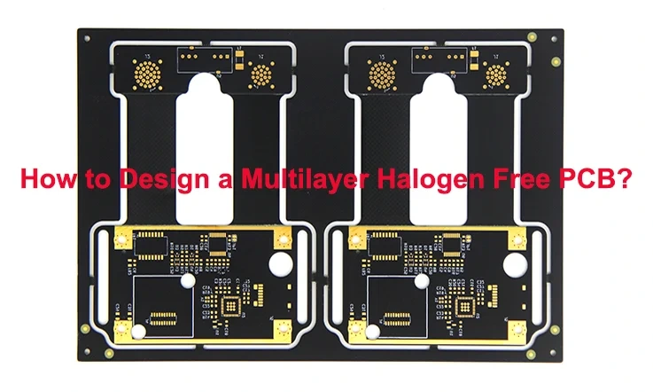
As the demand for environmentally friendly and high-performance multilayer halogen-free PCBs continues to rise, human are focusing on developing sustainable, reliable, and efficient circuit boards. This guide delves into the technical aspects of designing, fabricating, and testing multi-layer halogen free PCBs, exploring the unique challenges and solutions in PCB manufacturing that come with using halogen-free materials. From understanding the intricate details of PCB construction to mastering the manufacturing process and ensuring top-tier quality control, this article provides a clear roadmap for achieving high-performance, reliable multi-layer halogen-free PCBs.
Therefore, if you are working in electronics manufacturing, designing custom PCBs, or overseeing production processes, this resource offers practical insights and strategies for optimizing your PCB production workflow.
What Are Multilayer Halogen-Free PCBs?
Multilayer halogen-free PCBs are printed circuit boards that are manufactured without the use of halogenated compounds like bromine or chlorine. These halogen-free materials are essential in today’s sustainable PCB manufacturing processes. Typically, multilayer PCBs have multiple conductive layers separated by insulation, enabling complex electronic devices to function in a compact and reliable manner.
In multilayer halogen-free PCBs, the use of halogen-free resin systems or laminates ensures a lower environmental footprint during manufacturing and end-of-life disposal. Eco-friendly PCBs are growing in popularity because they not only comply with RoHS (Restriction of Hazardous Substances) but also meet the increasing demand for sustainability in electronics manufacturing.
For example, a consumer electronics manufacturer who is required to use halogen-free PCBs to meet regulatory standards in markets like Europe and North America. By adopting multilayer halogen-free PCBs, they not only stay ahead of the curve but also ensure the product’s recyclability and safe disposal, which is becoming a more significant concern in today’s green-conscious consumer market.
Importance of Halogen-Free Materials in PCB Manufacturing
Now that we know what multilayer halogen-free PCBs are, let’s zoom in on why these materials have become so in-demand in the PCB manufacturing industry. The shift toward halogen-free materials is driven primarily by environmental concerns and industry regulations.
Halogenated compounds like bromine and chlorine are toxic and can be harmful to the environment, especially when electronic waste ends up in landfills. When halogen-free PCBs are disposed of improperly, the environmental damage is minimized because these materials don’t release harmful gases or toxic elements. This is a big win in our fight against e-waste and pollution.
RoHS (Restriction of Hazardous Substances) regulations have had a significant impact on industries looking to export to EU markets. These regulations prohibit the use of certain hazardous substances, including bromine and chlorine, which has led many manufacturers to shift to halogen-free alternatives. This has sparked a wider adoption of halogen-free PCBs across various industries, particularly consumer electronics, automotive, and medical devices—all of which require eco-friendly PCB solutions for compliance.
Let’s take a look at an example. Apple, a leader in consumer electronics, has already phased out halogenated materials from its products, including halogen-free PCBs, as part of its sustainability efforts. This not only aligns with RoHS standards but also boosts the company’s image as an environmentally conscious brand.
How Multilayer Halogen-Free PCBs Meet Industry Standards?
When it comes to multilayer halogen-free PCBs, meeting industry standards is not just a formality—it’s a necessity. Compliance with RoHS and other global environmental standards ensures that halogen-free PCBs are both safe for use and environmentally responsible. Let’s break down how these PCBs meet the rigorous standards set by regulatory bodies:
1.RoHS Compliance: As we mentioned earlier, RoHS plays a massive role in pushing manufacturers towards halogen-free PCBs. The directive limits the use of hazardous substances in electrical and electronic equipment, including brominated flame retardants. By using halogen-free materials like FR-4 laminates, manufacturers ensure that their products are RoHS-compliant.
2.UL Certification: Another industry standard that multilayer halogen-free PCBs need to meet is UL (Underwriters Laboratories) certification. UL is recognized for evaluating the safety of electronic materials and products. Halogen-free PCBs that have received UL certification have been tested for their resistance to fire, high temperatures, and electrical performance. This certification ensures that these PCBs are reliable for use in demanding applications like automotive electronics, where safety and reliability can’t be compromised.
3.ISO Standards: Manufacturers producing multilayer halogen-free PCBs also strive to meet global quality standards like ISO 9001 and ISO 14001. ISO 9001 ensures that manufacturers maintain consistent quality throughout their production processes, while ISO 14001 focuses on managing environmental impact. These certifications help manufacturers guarantee that their eco-friendly PCBs are produced under well-regulated and sustainable practices, making them more attractive to industries focused on both quality and environmental responsibility.
●Example: Companies like Samsung and Panasonic are well-known for meeting these rigorous standards, and they rely on halogen-free PCBs to ensure their products are compliant, high-quality, and eco-friendly. When these companies choose multilayer halogen-free PCBs, they aren’t just meeting compliance standards—they’re pushing the industry toward more responsible manufacturing practices.
Advanced Manufacturing Processes for Multilayer Halogen-Free PCBs
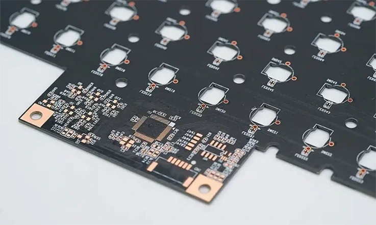
The production of multilayer halogen-free PCBs relies on a well-coordinated series of processes designed to deliver high-performing and environmentally conscious circuit boards. As human are increasingly focusing on eco-friendly designs, understanding how multilayer halogen-free PCBs are produced is more relevant than ever. The PCB manufacturing process for these boards is distinct, involving special materials, precise steps, and a deep understanding of both performance and sustainability.
Let’s walk through how the PCB fabrication process works for multilayer halogen-free PCBs, including the material choices, layering techniques, and the challenges faced during production. This detailed breakdown will give you insight into how us tackle these demands head-on.
The PCB Manufacturing Process for Multilayer Halogen-Free PCBs
The journey of multilayer halogen-free PCBs begins with selecting the right PCB materials and progresses through various stages of fabrication. This step-by-step process is fundamental to ensuring the boards meet both performance requirements and environmental guidelines. Here’s an in-depth look at each step involved in manufacturing these eco-friendly boards:
1.Material Selection and Preprocessing-
●At the start, we can choose halogen-free materials like halogen-free FR4 or polyimide based on the design’s thermal and electrical needs. These materials are then cut into sheets and prepped for the next stage.
●The materials are cleaned to ensure there are no contaminants before proceeding to the layering process.
2.Design and Etching-
●Once the PCB design is finalized, it is transferred onto the laminate using laser imaging or photoresist techniques. This design defines the trace paths, vias, and other conductive elements.
●Next, the board undergoes etching to remove unwanted copper, leaving the desired patterns behind for the circuit pathways.
3.Layering and Pressing-
●For multilayer PCBs, several layers of etched copper and resin are stacked together. Prepreg materials (resin-soaked fiberglass) are added between the layers to bond them and provide structural integrity.
●The layers are then laminated under heat and pressure to ensure a solid bond between each layer.
4.Drilling and Plating-
●The next step involves drilling holes for vias—these holes create the vertical connections between the layers. The drilled holes are then plated with copper to form reliable electrical pathways between layers.
5.Solder Mask and Surface Finish-
●After plating, a solder mask is applied to protect the board and prevent short circuits. In halogen-free PCBs, this mask is made from environmentally friendly materials, further reducing the PCB’s environmental impact.
●The final surface finish, often ENIG (Electroless Nickel Immersion Gold), is applied to ensure smoothness and improve corrosion resistance.
6.Final Testing and Inspection-
●Once all layers are completed, the multilayer halogen-free PCB undergoes various electrical and mechanical tests. These tests check for continuity, integrity, and overall reliability, ensuring the board meets industry standards for performance and safety.
Material Selection and Layering for Multilayer Halogen-Free PCBs
The materials selected for manufacturing multilayer halogen-free PCBs directly influence both the performance and environmental footprint of the finished product. These materials affect various factors, including thermal management and electrical performance, which makes selecting the right ones a main consideration in the production process. Choosing the correct materials can ensure the board operates efficiently while meeting eco-friendly standards—so it’s something we need to pay close attention to.
1.Halogen-Free Resins-
●Halogen-free FR4 is one of the most commonly used materials for multilayer PCBs, and it replaces traditional brominated or chlorinated resins with non-halogenated alternatives. Materials such as phosphorus and magnesium hydroxide are often used to achieve flame resistance without the environmental concerns associated with halogens.
●Another material option, polyimide, offers excellent thermal stability and is often used in flexible or high-temperature applications.
2.Copper Clad Laminate (CCL)-
●The core material for halogen-free PCBs is copper, which forms the conductive pathways. Copper is often electroplated onto the board, ensuring uniformity and excellent conductivity.
●Copper-aluminum alloys may be used in cases where the PCB needs to be lightweight or requires more signal strength.
3.Prepreg Materials-
●The prepregs used in multilayer PCBs are essential for bonding multiple layers together. These resin-soaked fiberglass materials provide not just structural integrity but also improve the board’s thermal conductivity.
●Prepregs are often layered between copper sheets, and the choice of prepreg material affects both performance and stability in the final PCB.
4.Solder Masks and Surface Finishes-
●A solder mask is applied to the PCB to ensure there’s no unwanted electrical connection, protecting the board from contaminants. For halogen-free PCBs, the solder mask is also made from eco-friendly materials.
●ENIG or HASL are common surface finishes used to protect the copper and enhance the board’s overall durability. ENIG is particularly useful for halogen-free PCBs due to its corrosion resistance and smooth finish.
Challenges in Fabricating Multilayer Halogen-Free PCBs
While multilayer halogen-free PCBs offer several advantages, the manufacturing process does come with its own set of challenges. These challenges, if not addressed properly, can hinder the efficiency and reliability of the final product. Here’s an exploration of some of the most common challenges:
1.Material Compatibility-
●Halogen-free resins can behave differently than traditional materials, making them more difficult to process. For example, these resins may require higher temperatures during lamination to achieve the desired bond strength.
●Solution: We need to invest in specialized equipment and refine our processes to adapt to the unique properties of halogen-free materials.
2.Thermal Management-
●In multilayer PCBs, heat management is a consistent concern. The multi-layered design can lead to heat being trapped within the PCB, which can impact the performance of sensitive components.
●Solution: Utilizing thermally conductive materials and incorporating vias specifically designed for heat dissipation can improve thermal management in halogen-free PCBs.
3.Increased Manufacturing Costs-
●Producing halogen-free PCBs often involves sourcing specialized materials and equipment, which can increase the overall cost of production.
●Solution: To offset these costs, we can streamline production processes, minimize waste, and improve material efficiency.
4.Meeting Regulatory Requirements-
●Halogen-free PCBs must meet a variety of regulatory standards, such as RoHS, UL certification, and other ISO standards. This can be especially challenging for companies working in diverse markets with differing compliance requirements.
●Solution: By keeping up-to-date with changing regulations and working with compliance experts, we can ensure our multilayer halogen-free PCBs meet all necessary requirements for global markets.
High-Performance Benefits of Multilayer Halogen-Free PCBs
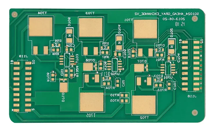
As industries push for sustainable and high-performing electronic components, multilayer halogen-free PCBs have emerged as a go-to solution for high-performance circuit boards. These advanced PCBs provide a solid foundation for demanding applications by offering both excellent electrical conductivity and effective heat management. Let’s take a deep dive into the specific benefits these boards bring, and how they address the challenges that come with modern electronic designs.
In high-performance environments, where signal integrity, heat dissipation, and durability are non-negotiable, multilayer halogen-free PCBs prove their worth. So, if you’re designing for IoT devices, medical technology, or high-frequency circuits, the performance characteristics of these PCBs must meet very precise standards. Let’s break it down further.
Electrical Conductivity and Signal Integrity in Multilayer Halogen-Free PCBs
When it comes to multilayer PCBs, one of the core considerations is signal integrity. With the complexity of modern circuits, ensuring that signals travel with minimal distortion and low resistance is a must. But how do halogen-free PCBs stack up when it comes to maintaining high-quality signals?
Signal Integrity-
Halogen-free materials used in multilayer PCBs offer strong electrical conductivity, helping reduce signal loss during transmission. Unlike traditional PCBs that rely on bromine- or chlorine-based compounds, halogen-free alternatives ensure that no harmful chemicals are present in the final product. This makes them a solid choice for industries focused on reducing environmental impact while maintaining high performance.
●Material Properties: Certain materials, like polyimide or halogen-free FR4, not only reduce environmental risks but also contribute to enhanced signal quality. These materials allow for cleaner electrical transmission and fewer interruptions or reflections, making them suitable for applications that require precision, such as telecommunications or medical devices.
●Trace Design: The fine trace design is also a reliable element in achieving low resistance and preserving signal integrity. Multilayer PCBs benefit from precise trace routing and via design that ensures minimal electrical resistance even as signals travel through multiple layers.
How Multilayer Halogen-Free PCBs Achieve Low Resistance-
●The layering design of multilayer PCBs helps with minimizing the distance signals travel through non-conductive regions, further enhancing signal integrity.
Here is a table that illustrates the electrical conductivity properties of different materials used in multilayer halogen-free PCBs:
| Material Type | Electrical Conductivity (S/m) | Maximum Operating Temperature (°C) |
| Halogen-Free FR4 | 5.0 x 10⁷ | 130 |
| Polyimide (PI) | 1.5 x 10⁶ | 300 |
| Epoxy-Glass Composite | 2.8 x 10⁷ | 130 |
Thermal Management in High-Performance Multilayer Halogen-Free PCBs
When it comes to high-performance PCBs, managing heat is non-negotiable. Excessive heat can lead to component failure, reduced lifespan, or unreliable performance. Multilayer PCBs are particularly adept at managing heat in high-performance environments due to their design flexibility and layered structure.
How Multilayer Designs Help with Heat Dissipation-
●Thermal Spreading: The multilayer structure of these PCBs allows for better heat distribution and dissipation. This is achieved by spreading heat across the layers and reducing the concentration of heat on a single layer, which can lead to failure.
●Via Connections: Thermal vias are used to channel heat from high-temperature areas directly to lower layers, where heat can be dissipated more effectively. By leveraging multiple layers, multilayer halogen-free PCBs manage heat more efficiently than single-layer boards.
●Material Choices for Heat Resistance: The halogen-free materials selected for these PCBs also impact their thermal characteristics. Materials like polyimide and halogen-free FR4 are known for their ability to withstand high temperatures without degrading, further enhancing the thermal stability of the PCB.
Example: In a high-frequency circuit like an RF amplifier, heat can easily accumulate, leading to performance degradation. With multilayer halogen-free PCBs, the inclusion of thermal vias and materials that resist heat buildup ensures consistent and reliable operation, even under heavy loads.
Here’s a table showing the thermal conductivity of materials used in halogen-free PCBs and their heat dissipation capability:
| Material Type | Thermal Conductivity (W/mK) | Thermal Expansion Coefficient (ppm/°C) |
| Halogen-Free FR4 | 0.35 | 15 |
| Polyimide (PI) | 0.12 | 25 |
| Epoxy-Glass Composite | 0.25 | 20 |
The Role of Multilayer Halogen-Free PCBs in Advanced Applications
Multilayer halogen-free PCBs are not just about basic functionality; they’re about meeting the demands of advanced applications where performance, signal integrity, and sustainability go hand-in-hand. Therefore, whether it’s for IoT devices, medical equipment, or high-frequency circuits, these PCBs are designed to deliver optimal performance in environments where other materials might fall short.
Advanced Applications and How Multilayer Halogen-Free PCBs Fit In:
1.IoT Devices-
●In the world of IoT, devices need to be compact, efficient, and able to process data quickly while consuming minimal power. Multilayer halogen-free PCBs meet these requirements by offering high-density designs with excellent signal transmission. Additionally, their eco-friendly nature fits the values of IoT product developers who aim for sustainability.
2.Medical Devices-
●Medical devices rely on precision and reliability. Multilayer halogen-free PCBs are an excellent choice for medical electronics because they reduce the risk of environmental toxicity while maintaining performance. So, whether it’s a wearable sensor or implantable device, these PCBs provide the necessary electrical conductivity and durability for medical applications.
3.High-Frequency Circuits-
●In high-frequency circuits, such as those used in 5G infrastructure or RF applications, maintaining signal integrity is a must. The multilayer design of halogen-free PCBs enables precise routing of signals, helping minimize loss and preserving the quality of data transmission.
Here’s a table showing the application areas and the specific requirements for multilayer halogen-free PCBs:
| Application Area | Signal Integrity Requirement | Thermal Management Requirement |
| IoT Devices | High | Moderate |
| Medical Electronics | High | High |
| High-Frequency Circuits | Very High | Very High |
Compliance with RoHS and Global Standards for Multilayer Halogen-Free PCBs
When creating multilayer halogen-free PCBs, compliance with global standards like RoHS and certifications from established bodies such as IPC and ISO are fundamental steps. These guidelines help ensure that the final product adheres to regulations and aligns with sustainability goals. Let’s explore how RoHS compliance, halogen-free certification, and adherence to IPC and ISO standards play a role in manufacturing multilayer halogen-free PCBs that meet industry requirements.
RoHS and Its Impact on Multilayer Halogen-Free PCBs
The Restriction of Hazardous Substances (RoHS) directive shapes the production of multilayer halogen-free PCBs by restricting certain materials that could harm both health and the environment. For halogen-free PCBs, RoHS compliance is a main aspect in eliminating hazardous substances from the manufacturing process, ensuring safer materials are used.
Understanding the Effect of RoHS on Multilayer Halogen-Free PCBs-
●Reducing Hazardous Waste: RoHS compliance limits the use of certain materials such as lead, mercury, and cadmium, contributing to a cleaner and safer manufacturing process for multilayer halogen-free PCBs.
●Regulatory Compliance: Following RoHS makes multilayer halogen-free PCBs eligible for global markets where environmental safety is a concern. For example, in the European Union, RoHS-compliant products are a requirement for the electronics industry.
●Environmental Responsibility: RoHS is not just about following laws—it’s about moving towards greener manufacturing and providing consumers with environmentally responsible products.
The table below lists the substances restricted by RoHS and their allowable concentration limits:
| Substance | Maximum Allowable Concentration |
| Lead (Pb) | 0.1% (1000 ppm) |
| Mercury (Hg) | 0.1% (1000 ppm) |
| Cadmium (Cd) | 0.01% (100 ppm) |
| Hexavalent Chromium (Cr VI) | 0.1% (1000 ppm) |
| Polybrominated Biphenyls (PBB) | 0.1% (1000 ppm) |
| Polybrominated Diphenyl Ethers (PBDE) | 0.1% (1000 ppm) |
Achieving Halogen-Free Certification for PCBs
Certification of halogen-free PCBs is a process that ensures no halogenated substances like chlorine, bromine, or iodine are present in the materials used. We must need to go through specific steps to acquire halogen-free certification for multilayer halogen-free PCBs.
Steps to Obtain Halogen-Free Certification-
1.Choosing Halogen-Free Materials: It starts with selecting materials that do not contain halogenated compounds, such as halogen-free FR4 or polyimide.
2.Production Techniques: During the PCB manufacturing process, care must be taken to prevent contamination from halogen-containing materials.
3.Testing for Compliance: Companies conduct several tests like X-ray fluorescence (XRF) or chemical analysis to ensure no halogenated substances exceed the prescribed limits.
4.Formal Certification: Once the PCB passes the tests, we can apply for halogen-free certification from trusted authorities like UL or SGS.
The testing methods listed below are commonly used to ensure halogen-free certification:
| Testing Method | Purpose | Details |
| X-ray Fluorescence (XRF) | Detects halogen presence | Non-destructive, quick analysis method |
| Fourier Transform Infrared Spectroscopy (FTIR) | Identifies halogenated compounds | Comprehensive analysis of chemical structure |
| Ion Chromatography | Measures ionic content | Used for accurate quantification of halogens |
How Multilayer Halogen-Free PCBs Meet IPC and ISO Standards?
IPC (Institute of Printed Circuits) and ISO (International Organization for Standardization) provide guidelines that focus on quality, safety, and performance in multilayer halogen-free PCBs. Following these standards ensures multilayer halogen-free PCBs are built to meet both customer requirements and global environmental expectations.
How IPC and ISO Standards Shape Multilayer Halogen-Free PCBs-
●IPC-2221: This standard provides comprehensive guidelines on the design and fabrication of printed circuit boards. Following these guidelines helps to ensure multilayer halogen-free PCBs are reliable in terms of performance, especially in applications requiring high electrical and thermal efficiency.
●ISO 9001: This certification assures manufacturers follow stringent quality management practices that optimize production, reduce errors, and improve customer satisfaction with multilayer halogen-free PCBs.
●ISO 14001: This environmental management standard ensures sustainable practices in production, including waste management, reduced energy consumption, and the use of environmentally friendly materials.
The table below shows how following IPC and ISO standards impacts the multilayer halogen-free PCB production process:
| Standard | Focus Area | Impact on Halogen-Free PCBs |
| IPC-2221 | PCB Design & Fabrication | Ensures robustness and reliability in PCB designs |
| ISO 9001 | Quality Management | Enhances consistency in production and customer satisfaction |
| ISO 14001 | Environmental Management | Promotes eco-friendly practices in PCB manufacturing |
Surface Finish Options for Multilayer Halogen-Free PCBs
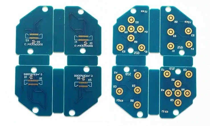
In the multilayer halogen-free PCB manufacturing process, surface finish plays a central role. It directly influences solderability, durability, and overall performance in the final application. Several options are available, such as Immersion Gold (ENIG), HASL (Hot Air Solder Leveling), and OSP (Organic Solderability Preservative). Each method has its own set of applications, advantages, and drawbacks.
The Role of Immersion Gold (ENIG) in Multilayer Halogen-Free PCBs
Immersion Gold (ENIG) is a surface finish technique commonly used in multilayer halogen-free PCBs. It involves the deposition of a thin layer of gold over a nickel substrate, creating a flat, corrosion-resistant surface ideal for high-density and precision applications.
Why ENIG is Commonly Used-
●Enhanced Solderability: The smooth, even surface of ENIG ensures excellent soldering results. This is especially true for halogen-free PCBs, where consistent soldering results are necessary to ensure accurate component placement and strong connections. ENIG supports effective performance, making it a popular choice for high-quality, environmentally-friendly boards.
●Corrosion Resistance: The gold and nickel combination offers superior resistance to oxidation, making it a go-to for applications requiring long-term durability and stable performance.
●Compatibility with Fine-pitch Components: ENIG provides a perfectly flat surface, which is suitable for high-density interconnections, such as fine-pitch components, where surface irregularities could affect solder joint quality.
Here is a quick comparison of ENIG with other finishes:
| Surface Finish | Advantages | Disadvantages |
| Immersion Gold (ENIG) | Excellent solderability, durable, smooth surface | Higher cost, more complex process |
| Hot Air Solder Leveling (HASL) | Cost-effective, widely used | Surface may not be flat, less suited for fine-pitch components |
| Organic Solderability Preservative (OSP) | Environmentally friendly, simple process | Less durable, sensitive to heat and moisture |
Comparison of Surface Finish Options for Halogen-Free PCBs
Choosing the right surface finish for your halogen-free PCB depends on several factors, including cost, performance, and the intended application. The three most common surface finishes—HASL, OSP, and ENIG—each have unique properties suited for different uses.
Surface Finish Options Breakdown-
●HASL: One of the most common and cost-effective finishes, HASL involves applying a layer of solder to the PCB and leveling it with hot air. While it is a tried and tested method, its uneven surface may not be suitable for high-density applications.
●OSP: This surface treatment provides a thin layer of organic material to preserve the copper surface until soldering. It’s an environmentally friendly choice but may lack the durability needed for long-term, high-performance applications.
●ENIG: As previously discussed, ENIG is ideal for precise, high-density connections, providing a smooth and corrosion-resistant finish that supports the reliable operation of multilayer halogen-free PCBs in demanding environments.
Here’s how each finish compares:
| Surface Finish | Cost | Solderability | Durability | Best Use |
| ENIG | Higher | Excellent | Long-lasting | High-precision, demanding applications |
| HASL | Low | Good | Moderate | General-purpose, bulk manufacturing |
| OSP | Moderate | Good | Limited | Environmental, low-cost applications |
Why Surface Finish Matters in Halogen-Free Multilayer PCBs?
When choosing a surface finish for multilayer halogen-free PCBs, the decision has a direct impact on several core factors like soldering quality, electrical characteristics, and overall board performance over time.. Understanding how each surface finish interacts with different materials in the PCB stack-up is necessary to ensure the best possible outcome for the specific application.
1.Surface Finish and Durability-
●Choosing the appropriate finish affects the PCB’s longevity and its ability to withstand harsh conditions. ENIG, with its smooth, durable gold layer, provides significant resistance to oxidation, making it an excellent option for long-term use. On the other hand, HASL’s uneven surface may affect its longevity in high-stress environments, especially where moisture or heat exposure is a factor.
2.Surface Finish and Performance-
●The right surface finish directly impacts the electrical performance of a multilayer halogen-free PCB. For example, a smooth surface like ENIG ensures stable electrical connections, while finishes with irregular surfaces, such as HASL, may cause slight variations in resistance that can affect signal integrity.
3.Environmental Considerations-
●OSP, being an environmentally friendly option, is suitable for industries prioritizing sustainability. However, it may not offer the same level of protection in high-temperature or high-humidity environments. For applications where environmental impact is a main factor, OSP offers a balance between eco-friendliness and performance.
Here’s how surface finish affects various aspects of halogen-free multilayer PCBs:
| Surface Finish | Durability | Electrical Performance | Environmental Impact |
| ENIG | Long-lasting | Stable, low resistance | Moderate |
| HASL | Moderate | May affect performance | High (due to lead content) |
| OSP | Moderate | Reliable for short-term use | High (eco-friendly) |
Multilayer Halogen-Free PCB Design Challenges and Solutions
Designing multilayer halogen-free PCBs brings a set of unique challenges, particularly when dealing with halogen-free materials. These boards often require a different approach compared to traditional PCBs, especially in terms of performance, routing, and manufacturing compatibility. Addressing these challenges efficiently is necessary to ensure that the PCB performs according to the required standards in the final application.
This section discusses the specific challenges in halogen-free PCB design and presents some solutions that can streamline the process while achieving optimal results.
Key Design Considerations for Multilayer Halogen-Free PCBs
When designing multilayer halogen-free PCBs, several elements need careful attention to guarantee that the board performs as intended. These include layer stacking, signal integrity, and power distribution.
1.Layer Stacking: Proper layer stacking helps minimize the PCB’s size while preserving its performance. For multilayer PCBs, the placement of signal and ground planes needs to be well-planned to reduce the risk of interference.
2.Signal Integrity: Maintaining signal integrity in halogen-free PCBs is a top concern, especially since these materials can behave differently than conventional ones. Materials with high dielectric constants can impact signal transmission, so careful routing is needed to preserve the signal quality over longer distances.
3.Power Distribution: The design of the power network on the PCB needs to be efficient. A good power distribution layout ensures that power reaches the appropriate components without causing noise or voltage drops, which could degrade performance.
Design Strategy for Layer Stacking-
●Alternating signal and ground layers can effectively reduce noise and interference.
●Multiple power planes help distribute current evenly and minimize thermal issues.
Here’s a quick look at how different layer configurations affect performance:
| Layer Configuration | Effect on Performance | Challenges |
| Signal / Ground / Signal | Helps reduce interference | Requires precise alignment |
| Signal / Power / Signal | Aids in signal integrity and power distribution | Increases routing complexity |
| Signal / Signal / Ground | Offers shielding and noise reduction | More complex to design |
Overcoming Challenges in Multilayer Halogen-Free PCB Routing
Routing within multilayer halogen-free PCBs can be challenging due to the physical and electrical characteristics of the materials involved. These challenges fall into two categories: electrical issues and physical routing concerns.
1.Electrical Challenges: When routing signals in halogen-free PCBs, managing signal degradation is one of the main concerns, especially for high-speed signals. Via-in-pad routing may help reduce signal travel distance, but it can also introduce signal reflection. Controlled impedance routing helps prevent this by ensuring a consistent impedance across the board.
2.Physical Routing Concerns: Halogen-free materials can behave differently from traditional PCB materials, affecting the way vias are drilled and layers are bonded. This requires attention to drilling sizes, soldering parameters, and layer alignment.
Routing Strategy to Address Challenges-
●Blind and buried vias are helpful in reducing space usage and minimizing signal interference.
●Impedance control is necessary to ensure signal integrity, especially in high-frequency applications where precise signal transmission is required. It helps manage the electrical characteristics of the PCB, reducing signal loss and interference for better performance.
| Routing Issue | Solution | Impact on Design |
| Signal Integrity | Controlled impedance routing | Helps preserve signal quality |
| Via size/placement | Use of blind and buried vias | Saves space and reduces interference |
| Material Compatibility | Adjust drilling and soldering parameters | Prevents issues with layer bonding |
The Importance of Design for Manufacturability (DFM) in Halogen-Free PCBs
Design for Manufacturability (DFM) is a design approach aimed at making sure that the PCB is easy to manufacture and can be produced cost-effectively. With halogen-free PCBs, this approach becomes even more relevant due to the unique properties of the materials used, which may require special handling or adjustments during the manufacturing process.
1.Via Types and Sizes: Minimizing the number of vias or opting for microvias can significantly reduce costs and simplify the manufacturing process.
2.Pad Designs: Ensuring that pads are correctly sized and optimized for the halogen-free PCB materials used will make the soldering process more reliable. These materials may behave differently compared to traditional boards, so ensuring compatibility is a must.
3.Drill Hole Sizes: Drill hole size compatibility with halogen-free materials is something that needs to be planned out at the beginning of the design phase. Matching the design specifications with the manufacturer’s capabilities helps avoid production delays.
DFM Tips-
●Reduce via usage and select microvia options where possible.
●Optimize pad designs to ensure effective soldering and prevent defects.
●Ensure drill hole sizes are suitable for the selected materials.
| DFM Consideration | Design Tip | Impact on Manufacturability |
| Via Count/Size | Minimize via usage, choose microvias | Reduces complexity and production time |
| Pad Design | Ensure pads are properly sized | Ensures reliable solder joints |
| Drill Hole Sizes | Match design to manufacturer’s drilling capabilities | Prevents delays and errors |
Ensuring Quality and Reliability of Multilayer Halogen-Free PCBs
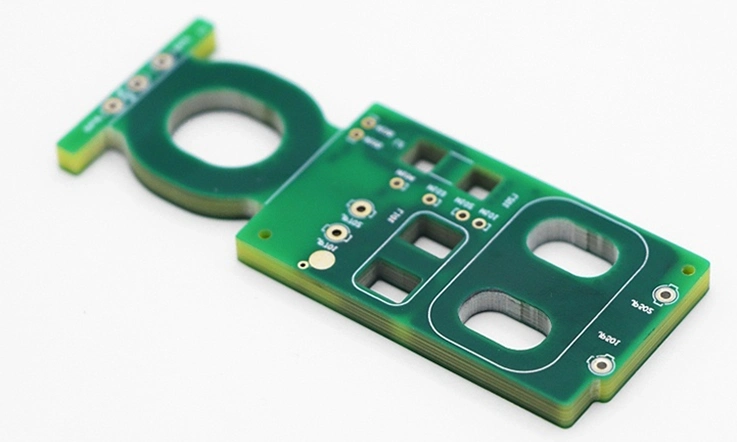
When manufacturing multilayer halogen-free PCBs, the pursuit of high quality and long-term reliability is a must. A PCB’s performance is directly influenced by the materials used, the design choices made, and how thoroughly it’s tested before it reaches the market. Halogen-free PCBs, in particular, require special attention due to their different characteristics compared to traditional PCBs.
In this section, we’ll dive into the testing and quality control processes that ensure these boards meet the expectations of our clients. Additionally, we’ll highlight how reliability testing helps confirm that halogen-free PCBs perform well over the long haul.
PCB Testing Methods for Halogen-Free Multilayer PCBs
Testing is a fundamental part of ensuring that halogen-free multilayer PCBs live up to their performance standards. Several methods are applied to evaluate the electrical, thermal, and mechanical aspects of the PCB.
1.Electrical Testing: This includes continuity testing and insulation resistance testing to verify the integrity of the electrical pathways. For halogen-free PCBs, electrical testing helps ensure that signal integrity remains intact, even when using alternative materials.
2.Thermal Testing: Halogen-free materials often have different thermal characteristics than traditional PCB materials. To evaluate how these materials handle temperature fluctuations, thermal shock and thermal cycling tests are performed. These tests help assess the PCB’s ability to manage temperature changes over time, which is especially useful for applications requiring stable thermal performance.
3.Mechanical Testing: Flexural strength and vibration testing are used to check the physical integrity of the PCB. These tests confirm that the board can withstand mechanical stresses that may occur during assembly, installation, or in the field.
Testing Approach for Multilayer Halogen-Free PCBs-
●Electrical Integrity: Use high-precision equipment to measure resistance and capacitance.
●Thermal Management: Conduct thermal cycling tests to simulate real-world conditions.
●Mechanical Strength: Subject the PCB to vibration and shock tests to assess structural durability.
Here’s an overview of common tests and their applications:
| Test Type | Purpose | Impact on Design |
| Electrical Testing | Ensures electrical signal integrity | Prevents signal degradation in high-speed applications |
| Thermal Shock Testing | Assesses temperature stability | Helps in applications exposed to fluctuating temperatures |
| Mechanical Testing | Measures physical durability | Guarantees that the PCB survives mechanical stress during use |
Quality Control Standards for Multilayer Halogen-Free PCB Manufacturing
Manufacturing multilayer halogen-free PCBs involves adhering to strict quality control standards. Whether it’s the materials selected or the production techniques used, having a clear process for PCB quality control helps ensure that all products meet the necessary specifications.
1.Material Quality: Ensuring that all materials used in the PCB are of high quality and compliant with industry standards is the first step. This includes testing for halogen-free certification and ensuring that the materials pass both environmental and electrical requirements.
2.Manufacturing Processes: Applying best practices in manufacturing, such as IPC standards and ISO certifications, ensures that every board is produced with consistency and precision. Every aspect of production, from PCB fabrication to assembly, should be monitored to avoid defects.
3.Inspection and Testing: Conducting visual inspection, automated optical inspection (AOI), and X-ray inspection at various stages of production helps catch any potential defects early. These inspections cover everything from surface finishes to inner layer alignment.
Quality Control Process-
●Incoming Material Inspection: Ensure that halogen-free materials are compliant with standards.
●Ongoing Process Monitoring: Use automated systems to track quality throughout the production stages.
●Final Inspection: Perform thorough checks before the PCB is shipped out.
| Quality Control Measure | Application | Impact on Reliability |
| Material Inspection | Verify material properties | Ensures consistency in performance |
| Process Monitoring | Track production stages | Detects and reduces defects early |
| Final Inspection | Comprehensive review before shipping | Guarantees the board is ready for use |
Reliability Testing and Stress Factors for Multilayer Halogen-Free PCBs
To assess the long-term reliability of multilayer halogen-free PCBs, stress testing is necessary to simulate the effects of prolonged use. Stress testing helps understand how the PCB will behave under different environmental and operational conditions.
1.Thermal Cycling: The PCB is exposed to temperature fluctuations that simulate real-world environmental conditions. This helps predict how the material will respond to high and low temperatures over time.
2.Mechanical Stress: Flexural testing and shock testing help assess the board’s structural integrity under mechanical stress, which is common during installation and use.
3.Environmental Stress: Some PCBs may be exposed to humidity or corrosive elements. Humidity testing and corrosion resistance testing determine how well the PCB can withstand such stress.
Reliability Testing Strategy-
●Simulate Real-World Use: Use thermal cycling to test for temperature extremes.
●Stress Resistance: Conduct mechanical and environmental tests to confirm reliability in various scenarios.
●Long-Term Durability: Perform tests to predict how the PCB will perform over the expected lifespan.
| Stress Test | Purpose | Expected Outcome |
| Thermal Cycling | Simulate temperature changes | Assess the PCB’s resistance to temperature extremes |
| Mechanical Stress | Evaluate physical durability | Verify the PCB’s resilience to mechanical forces |
| Environmental Stress | Test resistance to humidity and corrosion | Ensure long-term performance in harsh conditions |
FAQs & Multilayer Halogen-Free PCBs
1.What materials are used in Halogen-Free PCBs?
Common materials include halogen-free laminates, epoxy resins, and copper, which are free of harmful substances like brominated flame retardants (BFRs).
2.Can Halogen-Free PCBs be used in high-frequency applications?
Yes, many halogen-free PCBs can be designed for high-frequency and RF applications, though material selection is key to achieving optimal performance.
3.How does temperature impact Multilayer Halogen-Free PCBs?
High temperatures can affect the stability and performance of halogen-free PCBs, but selecting materials with good thermal resistance can mitigate this issue.
4.Do Halogen-Free PCBs have lower performance than traditional PCBs?
No, with proper design and materials, halogen-free PCBs can achieve performance levels comparable to traditional PCBs, especially for high-reliability applications.
5.How do I ensure my PCB is certified as Halogen-Free?
You need to select appropriate halogen-free materials and have the PCB undergo certification tests to confirm it meets standards like IEC 61249-2-21 for halogen-free products.

