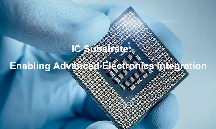
IC substrates form the foundation that connects semiconductor components to complex circuit boards. As industries like AI, IoT, 5G, and high-performance computing (HPC) continue to push for faster and more efficient devices, these substrates help ensure that the final products meet the demands of high performance, reliability, and compact design.
This comprehensive guide offers an in-depth look at the essential elements of IC substrate design, including the materials, manufacturing processes, and the specific technologies that enable them to support advanced packaging solutions such as flip-chip and high-density interconnects (HDI).
Introduction to IC Substrates: The Foundation of Advanced Electronics
In today’s world of high-performance electronics, the term “IC substrate” often doesn’t get the attention it deserves. However, these components are at the heart of advanced PCBs and play an indispensable role in modern electronic systems. As the push for more powerful, compact, and energy-efficient devices continues, the evolution of IC substrate technology will play a huge role in driving innovation.
IC substrates are designed to meet the high demands of advanced electronics by providing the necessary structure, electrical pathways, and thermal management required to ensure reliable and efficient device performance. They serve as the fundamental building block for IC packaging, PCB interconnects, and chip-to-board connections.
What is an IC Substrate? Defining Its Role in Electronics?
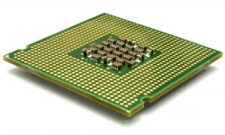
At their core, IC substrates are multi-layered boards used in PCB design that support integrated circuits (ICs). They provide the physical structure needed to create the electrical connections between the chip and the board, allowing for communication with other components in a system. More than just a base for the IC, these substrates are designed to ensure the smooth transmission of signals and to maintain the thermal balance of the system.
When you think about a smartphone or a 5G base station, the IC substrates inside these devices serve as the foundation for the components that make these devices function. For example, the IC substrate in a 5G base station has to be capable of handling high-frequency signals with minimal signal loss. In the case of AI chips, the IC substrate needs to ensure that the signals passing through it don’t degrade, keeping high-speed data transfer efficient and reliable.
Key Characteristics of IC Substrates in Modern Electronics
When we talk about IC substrates, there are a few standout features that truly define how these components perform in today’s high-demand applications. Let’s break down these main characteristics:
●Signal Integrity: For IC substrates to function effectively, they must maintain signal clarity. This is especially true for high-speed applications like AI chips and HPC systems, where even the smallest distortion in signal quality can lead to significant performance loss. Substrates need to support fast signal transmission without interference, and this requires careful material selection and precise routing.
●Thermal Management: As electronic devices become increasingly powerful, heat management has become a top concern in design. IC substrates are engineered with thermal control in mind, utilizing materials like ceramics or high-performance polymers that efficiently dissipate heat. Take AI processors, for example—they can generate a lot of heat, and without effective heat management, performance could drop off quickly. That’s where thermal vias and heat sinks come into play. These components are built into the substrate to channel heat away from critical parts, ensuring the system stays within the optimal operating temperature and continues to perform at its best.
●Reliability and Durability: The modern demand for long-lasting devices that can operate in challenging environments (such as extreme temperatures, moisture, or mechanical stress) has driven the development of more reliable IC substrates. High-end PCBs and IC substrates need to endure rigorous conditions without degrading, ensuring that systems perform well over extended periods of time.
Why IC Substrates Are Important for Cutting-Edge Technologies?
As electronics continue to evolve, IC substrates are becoming the foundation that enables these advancements. In this section, we’ll explore how IC substrates support some of the most cutting-edge technologies.
●AI and Machine Learning: The rise of AI technologies has led to an increased demand for high-performance processors that can handle complex calculations at scale. IC substrates in AI processors must be capable of supporting high-density connections and rapid data transfer while keeping heat under control. Substrates need to integrate fine-pitch designs and multiple signal layers to meet the high demands of machine learning and neural network processing.
●5G and Next-Gen Networks: As 5G technology expands, the need for robust IC substrates grows. These substrates must support high-frequency signals and high-density interconnections to maintain the speed and efficiency of next-gen communication networks. With 5G base stations and smart devices requiring precision and reliability in signal processing, IC substrates ensure these devices can meet demanding network requirements without performance degradation.
●High-Performance Computing (HPC): Systems designed for high-performance computing often feature multiple processors that run intensive computations. To achieve this level of performance, IC substrates are designed to manage high thermal loads and ensure signal fidelity across multiple processing units. Whether in cloud data centers or scientific research computing, these substrates play an integral role in ensuring that the system runs effectively under pressure.
Materials for IC Substrates: Choosing the Best for High-Performance Applications
In the design of IC substrates for high-performance electronics, selecting the right material can significantly influence the final product’s overall effectiveness. The decision goes beyond just cost; it’s about ensuring that the substrate provides the necessary characteristics like signal integrity, thermal management, and mechanical support for the application at hand.
IC substrates must be tailored to meet specific performance demands. AI processors require fast data processing with efficient power distribution, while 5G systems need materials that ensure low latency and consistent signal transmission. As technology pushes the boundaries of what’s possible, new materials and methods are continually developed to meet these evolving requirements. Let’s delve into the two broad categories of materials used for IC substrates and how their properties directly affect performance.
Organic vs Inorganic Materials: Understanding IC Substrate Materials
In the selection of IC substrate materials, two broad categories stand out: organic and inorganic materials. Each type is chosen based on the demands of the specific application and the environment in which the device will operate.
●Organic Materials (e.g., ABF Resin): Organic substrates, such as those made from ABF (Ajinomoto Build-up Film) resin, are often used in consumer electronics and mid-range devices. These materials are flexible, cost-effective, and allow for high-density interconnects that are often required in modern electronic devices. ABF resin, for example, enables designs with fine-pitch connections and is effective in handling moderate thermal performance. This makes it a preferred choice for IoT devices and smartphones, where power consumption and miniaturization are prioritized.
●Inorganic Materials (e.g., Glass Substrates): Inorganic materials, like glass substrates, are known for their excellent thermal conductivity and dimensional stability, making them a solid choice for applications involving high temperatures and intense workloads. Glass substrates are commonly used in high-performance computing (HPC) systems and 5G infrastructure, where their ability to handle high-frequency signals and manage heat effectively supports smooth operations. These materials help maintain signal integrity and facilitate reliable data transfer, even in demanding environments.
Here’s a comparison table to summarize these materials:
| Material Type | Typical Applications | Advantages | Key Characteristics |
| Organic (ABF Resin) | Consumer electronics, IoT devices | Flexible, lower cost, high-density routing | Fine-pitch designs, moderate thermal performance |
| Inorganic (Glass) | HPC systems, 5G infrastructure | High thermal conductivity, excellent signal integrity | Signal stability, high-frequency handling |
High-Performance Materials for AI and IoT IC Substrates
With the increasing complexity of AI and IoT devices, material selection plays a large part in determining how well these systems operate. The materials used in IC substrates for these applications need to manage high-density interconnections and maintain efficient power distribution while ensuring that signal integrity is preserved under demanding conditions.
●AI Chips: For AI systems, which involve tasks like deep learning and neural networks, IC substrates must handle high-speed data processing without overheating. Materials such as polyimide and ABF resin are frequently used due to their ability to withstand high-frequency signals and thermal loads. These materials help to ensure low signal loss and maintain reliable communication between the various processing units within the AI chip.
●IoT Devices: IoT devices—ranging from smart sensors to wearable tech—require IC substrates that facilitate low power consumption while supporting multiple communication protocols. Materials like FR4 are commonly used in less demanding IoT applications, as they balance cost and performance. However, for industrial IoT or smart city applications, higher-end materials like ceramic substrates or polymides may be used to meet the demands of durability and stability in fluctuating temperatures and environments.
How Material Selection Affects Thermal Management and Signal Integrity?
When designing an IC substrate, thermal management and signal integrity are among the main factors in selecting materials. Each material has specific properties that impact how well the substrate addresses these aspects.
●Dielectric Constant: The dielectric constant of a material governs how it interacts with electrical signals. A material with a low dielectric constant is preferable when signal integrity is a primary concern, especially for high-speed systems like 5G and HPC applications. Lower dielectric constants reduce signal loss and prevent interference, allowing for more precise and faster data transmission.
●Thermal Conductivity: As electronic systems, particularly AI chips and HPC systems, produce significant amounts of heat, the ability to dissipate heat efficiently becomes necessary. Inorganic materials, like ceramics, have higher thermal conductivity, which helps in transferring heat away from sensitive components. This can prevent issues like thermal throttling, where components reduce performance due to excessive heat. On the other hand, organic materials tend to have lower thermal conductivity and are more suitable for applications where heat management isn’t as challenging.
●Signal Loss: Signal loss is another factor that influences IC substrate performance. Materials with low signal loss are preferred in high-frequency systems, such as 5G, where clear signal transmission is needed for smooth data flow. Ceramics are often chosen for these applications due to their low attenuation properties, helping to maintain the strength and quality of high-speed signals.
Here’s a summary of material properties that affect performance:
| Material Property | Effect on Performance | Material Example |
| Dielectric Constant | Affects signal transmission and speed | Low in ABF resin, polyimide |
| Thermal Conductivity | Affects heat dissipation and stability | High in ceramics, glass |
| Signal Loss | Influences signal integrity at high speeds | Low in ceramics, polyimide |
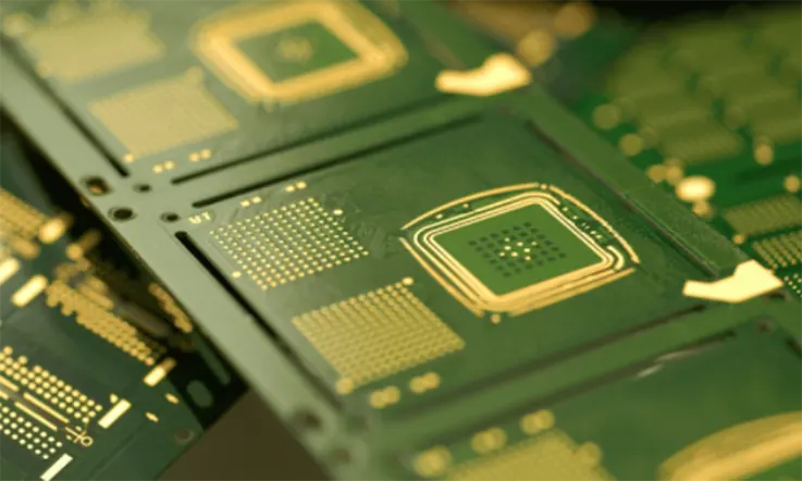
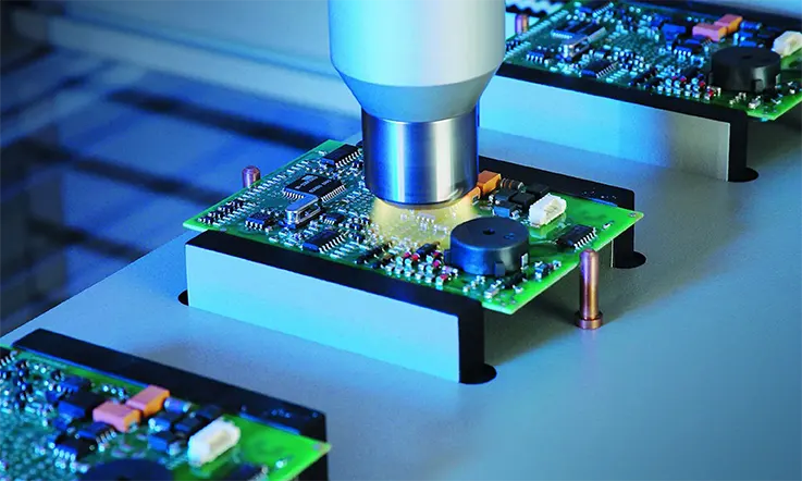
IC Substrate Manufacturing Processes: Precision Engineering for Performance
The manufacturing of IC substrates is a highly specialized process requiring advanced techniques to achieve the precision necessary for high-performance electronics. As devices get more complex, we must employ increasingly sophisticated methods to create substrates that can handle the demands of AI, IoT, and high-speed data transmission.
The manufacturing process must consider several factors, including the material selection, the complexity of the substrate design, and the precision required for producing microvias, fine-pitch traces, and stacked layers. These processes need to deliver substrates that meet the most stringent standards for signal integrity, thermal management, and mechanical durability. Let’s explore how these advanced manufacturing techniques come together to create high-performance IC substrates that support today’s innovative technologies.
Advanced IC Substrate Manufacturing Techniques
Manufacturing IC substrates involves a series of detailed processes to ensure optimal performance at the smallest scales. Techniques like microvia drilling, etching, stacking, and layer bonding are used to create high-density designs that support advanced electronic circuits.
●Microvia Drilling: One of the most main processes in modern IC substrate production is microvia drilling. These microscopic holes are created to facilitate high-density interconnections within the substrate. Typically, microvias range in size from 50 to 150 microns in diameter and are essential for connecting multiple layers of the substrate while keeping the footprint small. This drilling is done with precision lasers, ensuring minimal thermal stress and maximum control.
●Etching: Etching involves the use of chemical processes to remove unwanted materials and create the intricate patterns required for signal routing on the substrate. By exposing the material to acid-based solutions, we can create circuit patterns that serve as the path for electrical signals. The etching process needs to be extremely controlled to avoid defects that can compromise performance, particularly when working with fine-pitch designs.
●Stacking and Layer Bonding: As substrates become increasingly complex, the need for stacked layers has risen. Stacking involves bonding multiple layers of material to create substrates with higher component density. This allows for multilayer interconnections and ensures that each layer can handle specific electrical tasks. The bonding process requires precision, especially when combining different materials, such as organic films with inorganic layers like glass.
These processes work together to create IC substrates that can handle the intense demands of modern electronic systems. The combination of layering, microvias, and etching provides the structural integrity needed for applications like 5G, AI, and HPC.
The Role of Automation in IC Substrate Production
The growing complexity of IC substrates has made automation a fundamental part of the production process. With the use of machine learning and robotics, automation is transforming how substrates are produced, improving precision and efficiency while reducing the risk of human error.
●Machine Learning in Manufacturing: Machine learning has found its way into PCB manufacturing to predict and improve processes. By analyzing data from production runs, these systems can identify patterns, optimize workflows, and predict maintenance needs. This helps ensure that production remains smooth and cost-effective while maintaining the high standards required for high-performance IC substrates.
●Robotics and Automation Systems: Robotics are used to handle tasks like material handling, inspection, and soldering with unparalleled precision. These automated systems significantly enhance the speed and efficiency of processes like stacking, bonding, and layer alignment. They also allow for much finer control during processes like microvia drilling or etching, ensuring consistency across batches and reducing the chance of defects.
●AI for Predictive Maintenance: Automation also extends to predictive maintenance. With AI-powered tools monitoring every step of the production process, manufacturers can identify potential issues before they arise. For example, soldering issues or material wear can be detected early, minimizing downtime and enhancing overall production efficiency.
The combination of automation and AI brings a new level of precision to IC substrate production, ensuring high yields, reduced waste, and consistent product quality.
Achieving Fine-Pitch Designs for Complex IC Substrates
As electronics advance, fine-pitch designs are becoming more common, especially in high-density IC substrates. Fine-pitch designs involve reducing the distance between interconnects and traces to less than 0.5 mm. These designs are ideal for applications such as AI chips, 5G systems, and HPC, where efficient data transfer and compact sizes are required.
●Fine-Pitch Routing: Fine-pitch routing involves the creation of tight interconnections between microvias and traces. This requires precision etching and careful planning to prevent signal interference or cross-talk. We must also account for thermal expansion and ensure that the substrate maintains its integrity over time as temperatures fluctuate.
●Via-in-Pad: One of the techniques used in fine-pitch design is via-in-pad technology. This technique places vias directly under component pads to allow for tighter spacing, which is particularly useful in high-density circuits. While this method provides more room for component placement, it requires careful handling during soldering and stacking processes to avoid defects.
●Microvia Designs: Microvias are used to route signals through multi-layer substrates, creating a compact layout for high-performance chips. These vias can be blind or buried, depending on the design requirements, and their precise creation helps ensure signal integrity and thermal conductivity are maintained. Microvia designs assist us in achieving the miniaturization needed for next-gen devices while preserving performance and durability.
Table: Comparison of Fine-Pitch Techniques
| Design Method | Use Case | Benefits | Challenges |
| Fine-Pitch Routing | High-speed, miniaturized circuits | Space efficiency, high-density routing | Signal interference, trace complexity |
| Via-in-Pad | High-density PCBs | Tighter component placement | Potential soldering issues, complexity |
| Microvia Designs | Multi-layer IC substrates | Minimizes signal loss, supports miniaturization | Manufacturing complexity, cost increases |
IC Substrate Design for High-Speed Communication and AI Chips
When designing IC substrates for high-speed communication systems, such as those used in 5G or high-performance computing (HPC), or for AI chips, the stakes are high. These applications demand precision and reliability, as they operate under conditions where signal integrity, thermal management, and electromagnetic interference (EMI) can all make a huge difference in performance.
As the complexity of these chips increases, so does the need for innovative IC substrate designs that address unique challenges. For instance, AI chips typically require tight signal traces and minimized latency, while high-speed circuits like those used in 5G need to handle high frequencies and high power dissipation. Let’s break down the main design aspects and their specific applications to meet these demands effectively.
Signal Integrity in IC Substrates for High-Speed Applications
Signal integrity is one of the most pressing concerns when designing IC substrates for high-speed applications like 5G, HPC, and AI chips. At these frequencies, even the slightest imperfections in the substrate or the traces can cause signal loss or interference, resulting in data corruption or performance degradation. Here’s how impedance matching and crosstalk reduction come into play to keep things running smoothly.
●Impedance Matching:Impedance matching is a technique used to align the electrical impedance of PCB traces with the source and load impedance. This helps to avoid signal reflection, which can cause degradation or distortion, especially at high frequencies. For AI chips or 5G circuits, where maintaining signal clarity is necessary, accurate impedance matching ensures that the signal stays clean and undistorted from the transmitter to the receiver. Achieving this requires the use of advanced simulation tools and precise trace width calculations in the design process.
●Crosstalk Reduction: When multiple signals are routed in close proximity on a substrate, they can interfere with each other, a phenomenon known as crosstalk. For high-speed data transmission, this interference can significantly affect signal integrity. To minimize crosstalk, designers often employ techniques like shielding, ground planes, and the proper spacing between signal traces. By ensuring that trace layouts are properly optimized, crosstalk is reduced, allowing AI chips or HPC systems to operate without data corruption or performance hits.
Table: Key Techniques for Enhancing Signal Integrity in High-Speed Substrates
| Technique | Purpose | Application | Benefit |
| Impedance Matching | Prevent signal reflection and distortion | AI, 5G, HPC circuits | Maintains signal fidelity, prevents data loss |
| Crosstalk Reduction | Minimize interference between signals | AI chips, high-speed circuits | Enhances signal clarity, reduces errors |
| Ground Planes | Isolate signal traces and reduce noise | 5G, high-speed communications | Improves signal quality, reduces EMI |
Thermal Management Strategies in IC Substrate Design
As AI chips and 5G systems operate at increasingly high frequencies, thermal management becomes a challenge. High-frequency chips generate heat, which must be dissipated efficiently to ensure reliable performance over time. Here are some strategies used to control heat and maintain optimal substrate performance:
●Thermal Vias: Thermal vias are small holes within the IC substrate that provide a direct path for heat to travel from one layer to another. This process is used to guide heat away from core components and distribute it more evenly across the board. By using multi-layer designs with thermal vias, heat dissipation is maximized, helping to prevent overheating and component failure in high-power circuits.
●Heat Sinks: Heat sinks are passive devices designed to absorb and dissipate heat generated by high-power components. These are often placed on top of components like power transistors or AI processors to reduce the amount of heat building up within the substrate. In combination with thermal vias, heat sinks are highly effective in managing thermal stress and ensuring long-term reliability of the substrate.
●Thermal Conductivity of Materials: The material selected for the IC substrate impacts the efficiency of heat management. Materials such as ceramics and advanced polymers, known for their high thermal conductivity, are often used to enhance heat distribution. This ensures that even under heavy workloads, the substrate stays within thermal limits, preventing potential issues like thermal runaway or damage to components.
Example Case: In a 5G base station, the heat dissipation needs are particularly high due to the high-speed signal processing required. Our engineers design the substrate with advanced thermal vias and metal-core PCBs, which help rapidly dissipate heat to prevent the 5G chip from overheating during peak usage.
Minimizing Noise and Enhancing Reliability in IC Substrate Designs
Noise and reliability issues in IC substrates can undermine performance, especially for demanding AI and high-speed circuits. Electromagnetic interference (EMI) can degrade signal quality and introduce errors in data transmission. Let’s dive into how noise reduction strategies and reliability-enhancing techniques work together to ensure consistent performance over time.
●Electromagnetic Interference (EMI) Shielding: EMI shielding is one of the most effective ways to minimize external noise that can disrupt signal transmission within an IC substrate. Therefore, many designers use various shielding techniques such as conductive layers and ground planes to block unwanted electromagnetic waves. These shielding structures prevent interference from nearby components, ensuring that AI processors and high-speed communication chips operate without degradation.
●Material Selection for Reliability: Choosing the right materials for IC substrates has a direct impact on the reliability of high-speed circuits. Materials like polyimide, ABF resin, and ceramic composites provide mechanical stability and thermal resistance, ensuring the substrate can withstand extended usage. Reliability tests, such as thermal cycling and mechanical stress tests, are commonly conducted to confirm that the substrate maintains its performance over time.
●Via and Pad Design: The design of vias and pads on the substrate directly impacts its reliability. Via-in-pad designs are used to improve component placement density while ensuring that the vias are robust enough to handle thermal and electrical stresses. The careful pad design ensures proper soldering and electrical connectivity, reducing the chance of failure during long-term use.
Challenges in IC Substrate Design
The design and manufacturing of IC substrates for high-performance circuits require precise engineering and meticulous attention to detail. Challenges like signal integrity, thermal management, and reliability testing need to be addressed effectively to ensure long-lasting performance in diverse applications.
In this section, we’ll explore the common challenges that arise during IC substrate design, including how to address issues related to signal integrity, thermal stresses, and advanced testing for substrate reliability.
H3: Overcoming Signal Integrity Issues in IC Substrate Design
Signal integrity is a fundamental aspect of IC substrate design. As devices become smaller and more powerful, ensuring the quality of high-frequency signals traveling through dense circuits is a growing challenge. Without proper management, issues like signal degradation, impedance mismatch, and noise interference can degrade overall performance, especially in high-speed applications.
To maintain signal quality, several techniques are employed:
●Impedance Matching: It’s essential to design traces with controlled impedance to ensure that signals travel through the substrate without significant reflection. Misaligned impedance leads to signal loss or distortion.
●Crosstalk Reduction: Using ground planes and shielding techniques helps mitigate electromagnetic interference (EMI) and crosstalk between adjacent signals.
●Signal Path Optimization: Shortening the signal paths and optimizing the routing of traces can reduce the loss of high-frequency signals.
Table 1: Impedance and Signal Loss Comparison
| Material Type | Dielectric Constant | Signal Loss | Impedance Control |
| FR4 (standard) | 4.5 | 0.2 dB/inch | Moderate |
| High-Speed FR4 | 3.5 | 0.1 dB/inch | Good |
| Ceramic-filled Resin | 3.0 | 0.05 dB/inch | Excellent |
| PTFE (Teflon) | 2.3 | 0.03 dB/inch | Excellent |
As seen in Table 1, choosing the right material is core to achieving low signal loss and optimal impedance control for high-frequency applications.
Addressing Thermal and Mechanical Challenges in IC Substrate Manufacturing
Thermal management is a major factor in IC substrate design. As the demand for higher performance in smaller spaces increases, IC substrates must be able to handle greater heat generation and mechanical stresses without compromising performance.
●Thermal Cycling: Repeated exposure to thermal cycles can cause substrates to expand and contract, leading to delamination and warping. To reduce this risk, high thermal conductivity materials are used to dissipate heat efficiently.
●Mechanical Stress: As substrates become smaller and more densely packed with components, warping or cracking can occur under mechanical strain. Employing reinforced materials or multi-layer designs can help prevent structural failures.
Table 2: Thermal Conductivity and Material Choice
| Material Type | Thermal Conductivity (W/m·K) | Coefficient of Thermal Expansion (ppm/°C) |
| FR4 | 0.25 | 12-15 |
| Polyimide (Kapton) | 0.12 | 20-40 |
| Ceramic-filled Resin | 1.0 | 5-10 |
| Alumina (Al2O3) | 30 | 7 |
Table 2 compares materials commonly used for IC substrates based on their thermal conductivity and coefficient of thermal expansion (CTE). The higher the thermal conductivity, the better the material is at dissipating heat, while a lower CTE reduces the risk of thermal stress and warping.
Advanced Inspection and Testing for IC Substrate Reliability
Ensuring the reliability of IC substrates is essential to avoid system failures during product lifecycles. Advanced inspection and testing methods help identify flaws that could compromise substrate performance.
●Automated Optical Inspection (AOI): This technology uses high-resolution cameras and image recognition algorithms to detect surface defects such as misaligned vias, cracks, or voids.
●X-ray Inspection: Internal defects that can’t be detected by surface inspection methods can be identified with X-ray imaging, which allows for inspection of the substrate’s inner layers and connections.
●Failure Analysis: Once potential defects are identified, failure analysis tools such as scanning electron microscopy (SEM) and focused ion beam (FIB) help engineers pinpoint the exact cause of the problem.
Table 3: Testing Methods and Defect Detection Capabilities
| Testing Method | Defects Detected | Detection Rate |
| Automated Optical Inspection (AOI) | Surface defects (misalignment, trace breaks) | 90% |
| X-ray Inspection | Internal defects (voids, soldering issues) | 95% |
| Scanning Electron Microscopy (SEM) | Microscopic defects (delamination, cracks) | 98% |
| Focused Ion Beam (FIB) | Internal and surface defects (layer misalignment, pinholes) | 99% |
In Table 3, we compare inspection techniques based on their ability to detect various types of defects and the detection rate for each method. This provides insight into how us ensure IC substrate reliability during the production process.
Advanced Packaging Techniques for IC Substrates
In the modern electronics manufacturing industry, IC substrates are central to the development and performance of advanced packaging techniques. These techniques drive the compactness and efficiency of high-performance chips used in industries such as AI, 5G, and automotive electronics. The packaging process ensures that the IC substrate can meet the electrical and mechanical demands of modern applications, including high-speed data transfer and thermal management.
To achieve these demands, various packaging strategies are employed, including flip-chip, BGA, HDI, and even 3D packaging. These processes allow for enhanced signal integrity, reduced size, and better thermal conductivity. Let’s dive into some of the most effective packaging techniques and how IC substrates help meet the increasing demand for compact, high-performance electronics.
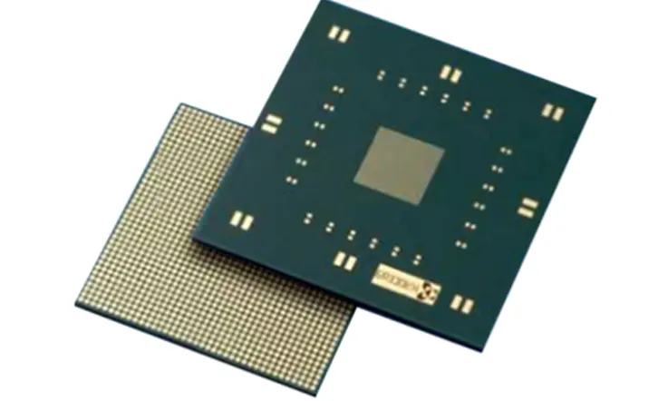
IC Substrates in Flip-Chip and BGA Packaging
When you look at modern electronics, flip-chip and BGA (Ball Grid Array) are two of the go-to packaging methods used to create compact, high-density circuits. These packaging methods are designed to handle the increasing demand for high-speed signals and reduced form factor, and both leverage IC substrates as the foundation for their performance.
●Flip-Chip Packaging: Flip-chip technology is widely used for its ability to enhance electrical performance by connecting the IC chip directly to the substrate with solder bumps. This design removes the need for wire bonds, which helps save space and shortens electrical paths. In devices like AI chips and 5G components, where clear signals and high-frequency operations are required, flip-chip technology minimizes signal loss and lowers parasitic inductance. IC substrates in flip-chip packages also assist in managing thermal stress, helping the chip function consistently during long operational hours.
●BGA Packaging: BGA packaging involves placing a grid of solder balls on the bottom of the IC substrate, which are then used to connect the chip to the PCB. It’s a widely used method in high-performance computing and mobile devices because it allows for more robust connections and better heat dissipation. With BGAs, the IC substrate provides a reliable interface that facilitates high-speed signal transmission while handling the heat generated by high-performance components.
Table: Key Packaging Techniques and Their Benefits
| Packaging Type | Key Features | Applications | Benefits |
| Flip-Chip | Direct connection, solder bumps | AI chips, 5G, high-speed chips | Lower parasitic inductance, high-speed performance |
| BGA | Solder balls for interconnection | Mobile devices, PCBs | Improved reliability, better thermal dissipation |
By using IC substrates, both flip-chip and BGA packaging can enhance the performance and reliability of chips, which is particularly beneficial for industries that demand advanced processing power, such as AI and 5G communications.
IC Substrate Solutions for High-Density Interconnects (HDI)
High-Density Interconnect (HDI) technology makes it possible to integrate more features into smaller spaces. HDI is a transformative method for creating compact, high-performance PCBs and IC substrates found in devices like mobile phones, wearables, and automotive electronics. Through the use of microvias and fine-pitch routing, HDI designs improve signal routing and enhance electrical performance in tightly packed systems.
●Microvia Technology: Microvias are tiny holes drilled into IC substrates to create connections between different layers in a PCB. They’re essential for high-density designs, enabling high-speed signal transmission in compact devices like smartphones and AI chips. The small size of these vias shortens the signal travel distance, which improves signal quality and reduces interference. In AI applications, where fast data processing is necessary, microvias help build dense interconnections while maintaining performance.
●Fine-Pitch Routing: Fine-pitch routing involves placing components with smaller spacing, enabling dense circuit designs. This approach allows IC substrates to support more components in a compact space, maintaining high-speed performance. The design ensures that signal paths remain short, minimizing signal loss and crosstalk, which could otherwise affect performance.
●HDI and AI Chips: For AI applications, HDI substrates ensure that AI chips with numerous connections function smoothly and responsively. These substrates support high-speed processing and manage complex data flows while helping with heat regulation.
Example Case: In an AI-driven autonomous vehicle, the IC substrates using HDI technology must support advanced processing and high-frequency communication without taking up too much space. Microvias ensure that the substrate can hold enough powerful ICs while ensuring signal quality and thermal dissipation.
3D Packaging and Hybrid Materials in IC Substrates
With the growing need for faster chips and higher densities, 3D packaging has emerged as a promising technology to take IC substrates to the next level. This innovation allows multiple layers of chips to be stacked on top of each other, significantly reducing the footprint of the substrate and enabling the miniaturization of electronic devices. Additionally, the use of hybrid materials in IC substrates enhances their overall thermal performance and signal integrity.
●3D Packaging: This technique involves stacking multiple ICs on top of each other in a vertical arrangement. The substrate acts as a support for each layer of chips, with micro-bumps providing connections between the layers. This allows for high-bandwidth data transfer between the stacked chips without significant signal degradation. For AI and HPC applications, 3D packaging offers a compact yet powerful solution for meeting the high-performance needs of next-gen computing systems.
●Hybrid Materials: Hybrid materials such as ceramic-filled polymers or graphene composites are increasingly being used in IC substrates to enhance thermal conductivity and signal integrity. These materials help manage heat more effectively, ensuring that chips in high-performance systems, such as 5G and AI applications, stay within operational temperature limits. Additionally, the versatility of these materials enables the design of more flexible packaging, which is especially beneficial in systems that demand curved or adaptable substrates.
●Integrating Flexible Materials: Another core innovation is the integration of flexible materials into IC substrates. This is particularly beneficial for applications like wearable electronics or flexible displays, where rigid PCB designs don’t work. The use of flexible substrates in combination with advanced packaging techniques allows for the creation of bendable or foldable devices without compromising on signal integrity or thermal performance.
Example Case: A next-gen AI chip designed for edge computing might require a 3D stacked configuration to maximize performance while reducing thermal stress. The IC substrate is designed with hybrid materials to ensure that heat generated by the stacked chips is efficiently managed.
IC Substrates vs. Substrate-Like PCBs (SLP), HDI, and Standard PCBs: A Comparative Analysis
The world of printed circuit boards is vast, and understanding the differences between IC substrates, Substrate-Like PCBs (SLP), HDI (High-Density Interconnect), and standard PCBs is essential for anyone working with high-performance electronics. These types of boards serve different purposes and are designed to meet specific requirements based on application needs, but what sets them apart?
This section will dive into the technical specifications of each type, comparing their design, layer count, thickness, and manufacturing characteristics. We’ll take a closer look at how these differences impact performance, particularly in cutting-edge fields like semiconductor packaging, 5G, AI, and IoT. By the end of this comparison, you’ll have a clearer picture of how to select the right PCB for your next project.
IC Substrates, SLP, HDI, and Standard PCBs: Key Differences in Design and Manufacturing
Let’s break down the distinctions between IC substrates, SLP, HDI, and standard PCBs, focusing on the number of layers, thickness, line width, and spacing—parameters that influence how these boards perform in different applications.
1.Layer Count and Complexity-
●IC Substrates typically range from 2 to 10 layers, designed with precision for semiconductor packaging.
●SLP also falls within 2-10 layers, but with a focus on reducing size and improving signal integrity while accommodating various active and passive components.
●HDI PCBs generally have 4 to 16 layers and are designed to handle high-speed signals with minimal interference, perfect for applications like mobile devices and advanced computing.
●Standard PCBs can stretch the layer count over 100 layers in some cases, depending on the complexity of the circuit. These are often used in traditional consumer electronics but are less suited for high-performance, high-speed designs.
2.Thickness Variations-
●IC Substrates are the thinnest of the group, often coming in at below 1.5mm, with some designs reaching as thin as 0.1mm.
●SLP boards are generally thicker than IC substrates but not as thick as HDI. Their thickness typically falls between 1.5mm and 3mm.
●HDI boards are thicker than SLP substrates, often ranging from 0.4mm to 7mm depending on the complexity and requirements of the end application.
●Standard PCBs can exceed 7mm in thickness, accommodating large, complex circuits or more rugged designs for industrial use.
3.Line Width and Spacing-
●IC Substrates are designed with line widths typically below 25μm (1mil), ideal for high-density designs where signal integrity is a top concern.
●SLP substrates offer a slightly more relaxed design but still support high-density routing with line widths above 1mil (typically in the range of 20-35μm).
●HDI PCBs are designed with line widths around 2mil (50μm), which allows for more complex routing and denser circuit designs compared to standard PCBs.
●Standard PCBs are the least dense in terms of line width and spacing, with widths typically above 2mil and limited to traditional designs with less compact routing.
Table 1: Comparison of Layer Count, Thickness, and Line Width for IC Substrates, SLP, HDI, and Standard PCBs
| PCB Type | Layer Count | Thickness | Line Width | Application |
| IC Substrates | 2-10 layers | <1.5mm | <25μm (1mil) | Semiconductor packaging, high-performance chips |
| SLP (Substrate-Like PCB) | 2-10 layers | 1.5mm – 3mm | 20/35μm | Active/passive components, precision electronics |
| HDI PCBs | 4-16 layers | 0.4mm – 7mm | 40-50μm | High-speed communication, mobile devices, medical electronics |
| Standard PCBs | >100 layers | >7mm | >2mil | Consumer electronics, industrial equipment |
●Analysis: This table offers a clear comparison of the layer count, thickness, and line width differences across various PCB types. These factors directly influence the choice of substrate based on the specific requirements of your application.
Technical Details of Substrate-Like PCB (SLP) and Its Role Between IC Substrates and HDI
SLP, also known as Substrate-Like PCB, has gained recognition for bridging the gap between IC substrates and HDI boards. Positioned between the two, SLP offers a balanced solution, allowing manufacturers to take advantage of smaller line widths and higher-density routing without fully embracing the complexity of HDI.
●Line Width and Spacing: One of the most significant advantages of SLP is its ability to reduce line width and spacing compared to standard HDI boards. While HDI typically supports line widths around 40-50μm, SLP can bring this down to as low as 20-35μm, allowing for denser routing and more compact designs.
●Design Flexibility: SLP’s ability to support smaller pitches and reduced trace widths makes it an attractive choice for high-performance consumer electronics, mobile devices, and wearable tech. It allows us to pack more functionality into smaller form factors, all while maintaining high reliability.
Table 2: SLP vs. HDI – Line Width Comparison-
| PCB Type | Line Width (μm) | Trace Pitch (μm) | Minimum via size (μm) |
| SLP | 20/35μm | 30μm | 60μm |
| HDI | 40-50μm | 50μm | 80μm |
●Analysis: As demonstrated in Table 2, SLP allows for smaller line widths and tighter trace pitches compared to HDI boards, making it a more cost-effective solution for high-density applications that don’t require the full complexity of HDI design.
IC Substrates vs. SLP, HDI, and Standard PCBs: Use Cases and Applications
Grasping the technical specifications is just one piece of the puzzle. It’s also necessary to align the right PCB type with the specific needs of the application. Below are some industries and use cases where each type of PCB is commonly applied:
●IC Substrates: Typically used in high-performance semiconductor packaging for chips, IC substrates are designed to meet the high-speed and low-volume requirements of advanced electronics. They are good for cutting-edge processors, memory modules, and 3D packaging.
●SLP (Substrate-Like PCB): With its higher density and flexibility, SLP is used in consumer electronics, smartphones, and wearable devices. Its ability to accommodate a variety of active and passive components makes it a go-to choice for compact yet high-performance boards.
●HDI PCBs: These boards are essential in high-speed communication systems, including 5G infrastructure, medical devices, and automotive electronics. Their superior signal integrity makes them perfect for applications where performance is non-negotiable.
●Standard PCBs: Standard PCBs are commonly used in traditional consumer electronics, home appliances, and industrial equipment. They’re the go-to choice when design complexity and speed aren’t the top considerations.
Why Choose Us for Fabricating Your IC Substrates PCB Project?
When it comes to fabricating IC substrates, achieving precision and performance is what sets your project up for success. Whether you’re in semiconductors, telecommunications, high-performance computing, or consumer electronics, selecting the right partner for PCB fabrication makes a real difference. We stand out in the competitive landscape by offering advanced technology, extensive experience, and a proven history of delivering high-quality IC substrates tailored to your specific needs.
1.Expertise in Advanced IC Substrate Designs and Manufacturing
With years of experience in the field, our team brings deep technical knowledge to every project. We specialize in signal integrity, thermal management, and high-density interconnects, ensuring your IC substrates perform as expected under varying conditions.
●Tailored Solutions: We can customize your IC substrates to fit everything from single-chip packaging to complex multi-layer designs, making sure each component functions seamlessly.
●Precision Engineering: We know how much of a challenge it can be to deal with signal loss, impedance mismatch, and the wear and tear caused by thermal cycling in your designs. That’s why we use the latest tools and tech to deliver the precision and reliability you need to keep things running at their best.
2.High-Performance Standards for Various Applications
Our IC substrates are designed to meet the demands of a wide array of high-tech applications. From 5G infrastructure to AI technologies, we build substrates that support the diverse needs of industries looking to stay ahead of the curve.
●5G Technology: We design substrates that are optimized for high-frequency and low-latency applications, ensuring your equipment works efficiently in 5G networks.
●AI and Machine Learning: As AI systems push boundaries, we provide IC substrates that are built to handle high-speed data processing while also maintaining thermal efficiency.
●Medical and Automotive Industries: With a focus on durability and reliability, our IC substrates provide stability and protection against electromagnetic interference, offering assurance in core applications.
3.Advanced Manufacturing Techniques for Maximum Precision
Our production capabilities cover everything from microvia drilling to laser etching, and we rely on advanced layer bonding techniques to meet the highest standards of PCB design. We’re equipped to handle complex designs with fine-pitch routing and high-density interconnects for applications that demand tight specifications.
●Microvia and Fine-Pitch Routing: With capabilities to produce microvias as small as 10μm and fine-pitch routing down to 20μm, we’re able to deliver substrates that meet the needs of today’s high-performance designs.
●Thermal Management Expertise: Our solutions for thermal vias and heat dissipation help ensure that IC substrates maintain optimal temperature control, even in demanding environments.
4.Rigorous Quality Control and Testing Processes
At every step of the manufacturing process, we apply a thorough testing regimen to verify the integrity and reliability of each IC substrate. We use automated inspection systems and failure analysis to identify potential issues before they arise, ensuring the highest level of reliability for every product.
●Automated Testing: Our in-line testing systems help identify and correct any issues early, guaranteeing that you receive consistent and reliable results.
●Comprehensive Reliability Testing: We rigorously test for factors such as thermal cycling, mechanical stress, and electrical integrity, ensuring that your IC substrates hold up in the long term.
5.Commitment to Sustainability and Cost Efficiency
We are dedicated to delivering cost-effective solutions without compromising on quality. Our lean manufacturing processes minimize waste and streamline production times, making sure we meet your budgetary requirements.
●Sustainable Practices: We embrace eco-friendly materials and energy-efficient processes, contributing to a more sustainable future while delivering reliable products.
●Competitive Pricing: We make sure our IC substrates provide great value, offering a balance of performance and cost, and ensuring that your budget is put to good use.
6.JarnisTech’s IC Substrate Manufacturing Capabilities
| Feature | Specification |
| Layer Count | 2 to 10 layers |
| Technology Highlights | PCB support for 1 chip solder via Wire Bonding or Flip Chip Process |
| Materials | BT (Bismaleimide Triazine) |
| Base Copper Thickness | 0-12μm depending on substrate structure method |
| Minimum Track & Spacing | 30/30µm (Advanced: 20/20µm) |
| Surface Finishes Available | ENIG & ENEPIG |
| Minimum Laser Drill | 50μm |
| Minimum Mechanical Drill | 100μm |
| PCB Thickness | 2L min. 130µm, 4L min. 210µm, 6L min. 300µm |
FAQ& IC Substrates
1. What is the maximum operating temperature for IC Substrates?
IC Substrates are generally designed to withstand temperatures up to 250°C, but this can vary depending on the materials used and the specific requirements of the application.
2. How do IC Substrates affect the performance of semiconductors?
IC Substrates provide a stable platform that ensures proper electrical and thermal performance of semiconductor chips. Their design influences factors like signal integrity and heat management.
3. Can IC Substrates support multi-chip packages?
Yes, IC Substrates can support multi-chip packages by providing complex interconnects between chips, often utilizing advanced features like microvias and multi-layer designs to ensure efficient communication.
4. Can IC Substrates be customized for different chip sizes?
Yes, IC Substrates are often custom-designed to accommodate specific chip sizes, ensuring optimal connectivity and signal integrity for each individual application.
5. Can IC Substrates be used for both active and passive components?
Yes, IC Substrates are designed to integrate both active (like semiconductors) and passive components (like capacitors and resistors) on the same substrate.
Related Posts:
1.Land Grid Array (LGA): Advantages, Challenges, Limitations, Applications
3.What Is RFID and Benefits of RFID in PCB Industry?
4.What Is FPGA and Why Do You Need to Care?