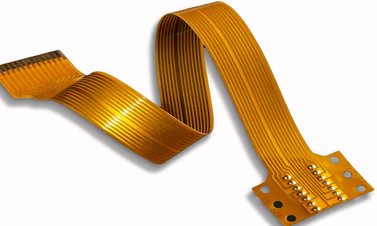
The evolution of Flexible Printed Circuit Boards has witnessed exponential improvements lately, rendering substantial market share growth and technological evolution. The emergence of innovative flexible PCB fabrication technologies has amplified the benefits of FPC, like minimal weight, sleekness, and adaptability, empowering them to secure extensive applications across various sectors.
As the performance of the substrate material is integral to the fundamental properties of printed circuit boards (PCB), enhancing substrate performance becomes crucial to improving the technical performance of the PCB, including its flexible variant.
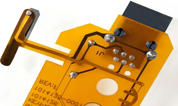
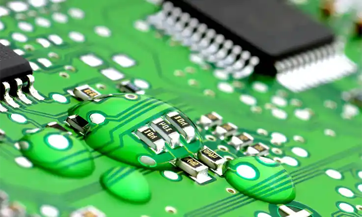
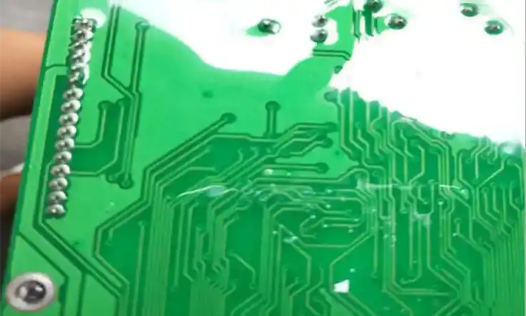
FPC, a type of flexible circuit board, is similar to traditional PCB in its function. FPC soft boards find extensive use in a variety of applications, including FPC antennas, flex PCB connectors, wireless charging coil arrays, and more. The composition of FPC primarily consists of flexible material that features high thermal stability and good electrical insulation properties
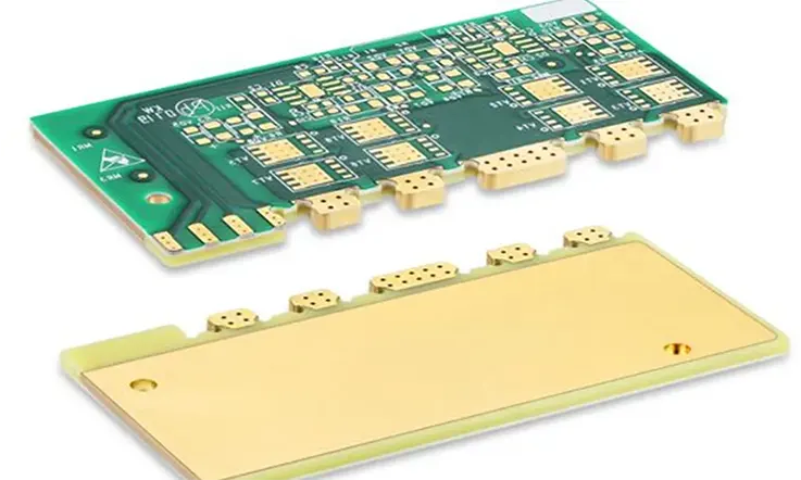
Material Composition of an FPC PCB
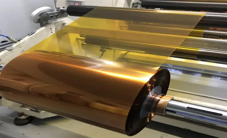
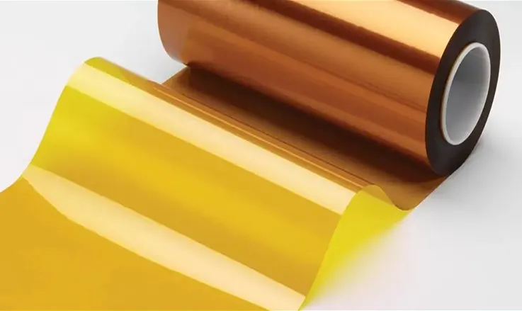
Insulating Substrate: The base substrate material is a crucial component in the manufacturing of both rigid and flexible printed circuit boards. It lays the essential groundwork on which the complete PCB configuration is constructed. For rigid PCB, FR-4 stands as the most widespread substrate material, whereas, for flexible PCB, polyimide (PI) film and PET (polyester) film are the typical materials. Additional polymer films, such as PEN (polyethylene nphthalate), PTFE, and Aramid, are also accessible.
●PI, a thermosetting resin, currently dominates in the fabrication of Flex PCBs. It is esteemed for its superior mechanical attributes, such as robust tensile strength, remarkable thermal stability (-200°C to 300°C), resistance to chemicals, exemplary electrical properties, extraordinary durability, and heat resistance. Additionally, it boasts unique flexibility features, unmatched by other thermosetting resins, even post-thermal polymerization. Nonetheless, PI resin displays a relatively reduced tear strength and moderate absorption of moisture.
●Conversely, PET resin boasts adequate electrical and mechanical properties; however, it is unsuitable for direct soldering as it exhibits poor heat resistance. PEN, another substrate material used in Flex PCB, provides medium-level performance, surpassing PET while not matching the quality of PI in terms of critical mechanical and electrical properties. Throughout the manufacturing process, Flex PCB manufacturers should employ the appropriate substrate material to ensure that the eventual PCB can function seamlessly for its intended application.
Liquid Crystal Polymer (LCP) Substrate: Liquid Crystal Polymer (LCP) substrate is rapidly emerging as a popular substrate material in Flex PCB. LCP is gaining immense popularity due to its ability to mitigate the limitations of Polyimide substrate while retaining all its features. LCP boasts a remarkable moisture or humidity resistance level of 0.04% while exhibiting a dielectric constant of 2.85 at 1GHz, making it ideal for high-speed digital circuits and high-frequency RF circuits.
●LCP substrate’s ability to address the inadequacies of other substrate materials has made it a staple in the Flex PCB manufacturing industry. Furthermore, the melted version of LCP, known as TLCP, can be injection molded and pressed to create a flexible PCB substrate that is readily recyclable.
Given the exceptional performance features attributed to LCP, Flex PCB manufacturers must consider integrating it as their preferred substrate material to manufacture high-performance Flex PCB to fulfill the demands of modern industries.
Adhesive: The adhesive sheet functions to adhere the film to the metal foil or to the film when dealing with the cover film. Various adhesive sheets can be utilized for diverse film substrates. For example, adhesive sheets devised for polyester substrates distinct from those employed for polyimide substrates, with the latter bifurcated into epoxy or acrylic types. The bonding sheet is generally selected based on its fluidity and coefficient of thermal expansion. Furthermore, copper-clad polyimide laminates that don’t require adhesive sheets call for lesser upkeep, boast superior chemical resistance, and showcase excellent electrical properties.
●The use of acrylic adhesive sheets poses a challenge as their low glass transition temperature leads to significant contamination during the drilling process, which is difficult to eliminate, thereby negatively impacting the quality of metallized holes. Subsequently, other adhesive materials are deemed inadequate for interlayer bonding sheets of multilayer flexible circuits. Hence, polyimide materials are commonly employed, which exhibit a consistent coefficient of thermal expansion (CTE) when paired with polyimide substrates, eliminating the issue of dimensional instability in multilayer flexible circuits. Furthermore, polyimide adhesive sheets possess exceptional mechanical and electrical properties.
Therefore, Flex PCB manufacturers must choose the right adhesive sheet for a given substrate type to ensure that the resulting PCB possesses the necessary mechanical, electrical, and dimensional stability to function correctly in its intended application.
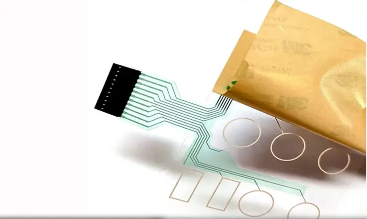
PI Cover Layer: The use of traditional PI/adhesive coverlay has not always sufficed in satisfying the needs of modern flexible PCB in terms of high density, dimensional stability, and environmental protection. Consequently, a more suitable alternative known as photo-imageable coverlay (PIC) with high flexibility resistance and comparable attributes to solder mask oil has been developed.
●Thus far, liquid or film-type PIC based on modified epoxy or acrylic resin has been extensively studied and applied due to its excellent binding force, high resolution, and flexibility. However, the limited dimensional stability of PIC based on modified epoxy or acrylic resin when used in high-density PCBs and its inferior Tg and heat resistance are notable shortcomings.
Flex PCB manufacturers must consider the factors affecting their desired outcome to choose the most appropriate coverlay material for the intended application. Consequently, the selection of coverlay materials should be conducted carefully with a focus on achieving the desired flexibility, environmental protection, and dimensional stability for the final product.
Flex PCB Stiffener: Stiffeners for flexible circuit boards are commonly categorized as follows: PI stiffener, FR4 stiffener, Steel stiffener, FED stiffener and others. The thickness of PI stiffeners may vary and is denoted by two values following “PI”, which indicate the thickness of PI and adhesive, respectively, both measured in Mil. These values can be adjusted according to the specific requirements of the customer. For instance, PI stiffeners may come in thicknesses ranging from PI1/2 1/2 to PI11, PI21, PI31, and up to PI91 depending on the customer’s needs.
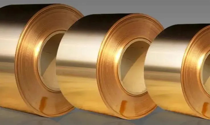
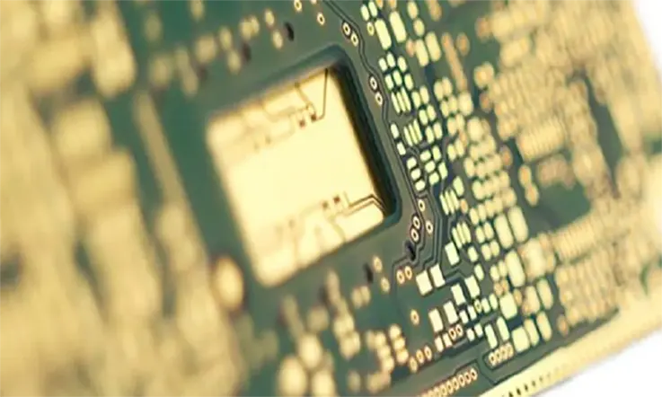
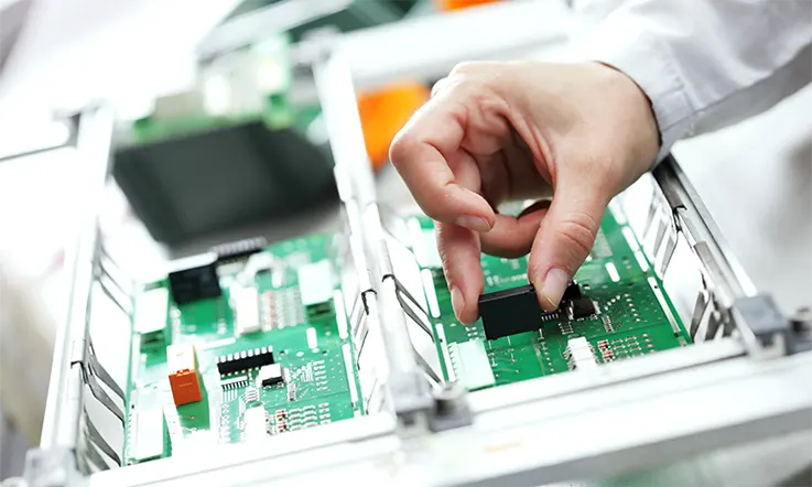
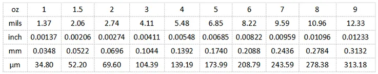
Copper Foil: Acting as a conductive layer, copper foil is meticulously adhered to an insulating base prior to the precision etching of conductive paths. The primary classes of copper foils in use are rolled and electrolytic copper foils. Showcasing superior malleability and resistance to bending, rolled copper foil offers elongation rates spanning 20% to 45%. In contrast, electrolytic copper foil provides an elongation range of 4% to 40%. A 35um (10z) thickness is standard for copper foils, though thinner variants like 18um (0.50z), and thicker renditions, such as 70um (2oz) or even 105um (30z), are also available.
●Electrolytic copper foil is formed via electroplating. The copper particle’s crystal state is such that it has a vertical needle-like shape, which makes it easier to produce vertical line edges during etching, which is advantageous in the manufacture of precision circuits. However, when the bending radius is less than 5m or when dynamic deflections are frequent, the use of needle-shaped copper particles is unsuitable. Rolled copper foil is usually used for flexible circuit substrates due to its malleable structure, featuring copper particles with horizontal shaft-like shapes that can accommodate numerous windings.
Therefore, Flex PCB manufacturers must carefully select the appropriate copper foil type considering several factors, such as flexibility and durability, among other aspects, to ensure the resulting design meets the specific application’s needs.
The Characteristics of Different Copper Foil Types Differ
The use of either rolled copper foil or electrolytic copper foil in Flex PCB manufacturing depends on several factors, including the desired properties of the final product. Although these two types of copper foils are produced using different methods, determining the superior choice can prove challenging.
When choosing the right type of copper foil, Flex PCB manufacturers must consider various design requirements, including flexibility, durability, and precision. Rolled copper foil’s superior ductility and bend resistance, coupled with its horizontal shaft-like copper particle shape, make it particularly suitable for flexible circuit substrates that accommodate numerous windings. In contrast, electrolytic copper foil features a crystal structure consisting of vertical needle-shaped copper particles, which makes it ideal for manufacturing precision circuits requiring vertical line edges during etching.
Ultimately, the selection of copper foil type is dependent on the specific application’s requirements, as the qualities of each type of copper foil offer distinct advantages in particular circumstances. Therefore, Flex PCB manufacturers must conduct careful assessments to determine the most suitable copper foil type and ensure that it meets the demands of the intended application, resulting in a successful end-product.
Two Types of Copper Foil
In some cases, Copper Sheet or Cu Copper may be referred to as a flexible circuit board material by older designers. However, it is worth noting that these terms represent distinct types of copper foil used in Flex PCB manufacturing.
Rolled Annealed Copper Foil or RA Copper Foil represents one classification of copper foil utilized in the fabrication of Flex PCB. Another frequently adopted variant in this context is Electrodeposited Copper, alternatively known as ED Copper Foil.
● ED Vs RA Copper Foil Cost: In regards to the cost of flexible circuit boards, we have found that the average cost of manufacturing using ED Copper Foil is lower than that of RA Copper Foil. However, if there are differing opinions, we welcome input and invite interested parties to reach out to JarnisTech directly.
● ED Vs RA Copper Foil performance: ED Copper Foil is comparatively fragile when compared to RA Copper Foil, and therefore more prone to breakage during the manufacturing process. In contrast, RA Copper Foil offers greater flexibility, making it the preferred choice for FPC copper foil.
When selecting the appropriate copper foil type for Flex PCB production, it is essential to consider several factors, such as durability, flexibility, and precision requirements, among other considerations. Consequently, Flex PCB producers must instigate thorough assessment procedures to pinpoint the optimal copper foil kind geared towards the target application. This meticulous selection process will pave the way for attaining the hoped-for specifications in the finalized Flex PCB product.
JarnisTech functions as a full-spectrum facilitator of manufacturing services for flexible PCB, encompassing facets from assembly and design to component procurement and product completion. With its foundation laid in 2002, JarnisTech’s functionality extends across two avant-garde PCB production facilities located in Jiangsu and Jiangxi, in addition to an fast PCB assembly factory based in Shenzhen.
We offer a broad range of flexible PCB, including yellow polyimide PCB with 1-12 layers, clear PCB with 1-10 layers, single/double-sided flexible PCB, flexible aluminum PCB, aluminum LED PCB, and HDI flexible PCB.
Here are some of the benefits of having JarnisTech produce your flexible PCB:
● JarnisTech provides turnkey manufacturing services for flexible printed circuit boards (FPC). Our services include FPC design, manufacture, PCB assembly, testing, and box-build assembly.
● We ensure high-quality flexible PCB production that meets strict industry standards such as ISO 9001, IATF 16949, UL, RoHS, and REACH.
● Our customers can benefit from our free and professional one-on-one engineering/design assistance for flexible PCB.
● For high volume flexible PCB/PCBA orders, we offer complete samples and PCBA functional testing to ensure the highest standards of quality.
● We stand behind our manufacturing services and provide quality money-back/free-rework assurance and traceable flexible PCB/PCBA fabrication.
FPC Design Guidelines and Considerations
Here are some possible FPC design guidelines and considerations:
● Bend Radius: The design approach for FPC necessitates cognizance of the bend radius to avert complications that could lead to material crack or fracture. Conventionally, the established minimum bend radius should ideally be proportionate to the FPC thickness, typically constituting a multiple of the same.
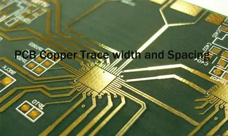
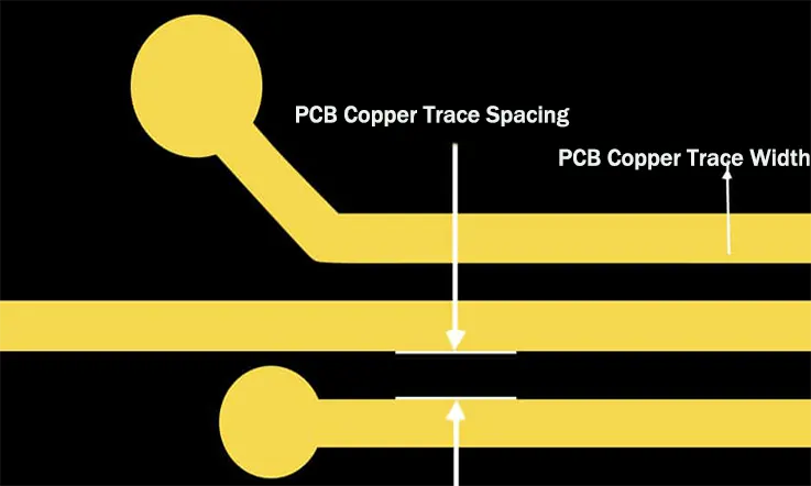
● Trace Width and Spacing: The trace width and spacing are critical factors to consider as they affect the electrical performance and can impact manufacturability. They are typically determined by the specific application requirements and should meet the manufacturer’s specifications.
● Material Selection: Flexible Printed Circuits (FPC) can be crafted from a variety of materials each possessing characteristics like thermal conductivity, flexibility and dielectric strength. Material selection should be based on the specific application requirements.
● Connection Points and Pads: The design of connection points and pads should align with the respective components and connectors slated for usage. The dimension and configuration of these zones should be crafted to facilitate robust and dependable connectivity.
● Solder Mask and Silk Screen: The solder mask and silk screen layers should be designed to ensure that they cover the appropriate areas of the FPC and do not interfere with the electrical performance or manufacturability.
● EMI Shielding: FPC can be susceptible to electromagnetic interference (EMI). Adding EMI shielding to the design can be important to minimize the impact of EMI on the electrical performance.
● Thermal Management: FPC can generate heat, which can impact electrical performance and reliability. Thermal management should be designed into the FPC to avoid overheating and damage to the components.
● Testing and Validation: It is important to test and validate the FPC design to ensure it meets the application requirements and is manufacturable. Testing can include electrical performance, mechanical stress testing, and environmental testing.
The Distinction Between PET and FPC
● Polyethylene Terephthalate (PET), a common polymer, is frequently utilized in the production of Flexible Printed Circuit Boards. With its significant transparency and restricted thermal expansion, PET establishes itself as an optimal selection for both solar modules and display panels. Conversely, FPC are immensely flexible entities, appropriate for an array of applications inclusive of high-functioning display panels and indoor uses.
● Flexible Printed Circuit Boards serve as an cost-effective solution that conserves crucial transportation space. The size of traditional rigid PCB can become unwieldy when populated with numerous components. In contrast, FPC are easy to fabricate and assemble, thanks to their flexible design.
● FPC are hybrids of integrated circuits(IC) and thin-film, printed circuit traces. Used in creating flexible circuit boards and electronic devices, FPC incorporate IC chips into thin, flexible plastic sheets. These circuits can be utilized in various applications,like solar panels, electric cars and aircraft, as well as emerging technologies such as aerial drones and wearable electronics.
● Applications of FPC continue to expand, and high-speed electrical circuits demand consistent electrical characteristics. As a result, FPC are relied upon for their ability to maintain signal integrity for a variety of applications, including cutting-edge technologies like aerial drones.
Flexible Printed Circuit Board (FPC) Applications
Flexible printed circuit boards have broad applications across various electrical and electronic sectors. Despite FPC offering versatility and adaptability, their cost is relatively higher than rigid PCB. Nonetheless, FPC have found widespread use in various industries, including:
●Automotive electronics
●Aerospace Components
●Electronics for computers
●Mobile Telephones
●Medical equipment
In addition to the industries mentioned above, flexible PCB are also used in wearable devices, digital cameras, and other applications. The notable benefits of these FPC encompass their flexibility, superior functionality, and multipurpose nature, rendering them perfectly suited for incorporation in sophisticated devices.
Advantages of FPC Board
The technology surrounding Flexible Printed Circuit Boards (FPC) presents numerous benefits making it a desirable choice across various applications. These are the distinct advantages offered by FPC technology:
●More flexibility
●Saves space
●High reliable
●Improved capabilities
●Cost effective
In summary, FPC technology offers greater flexibility, space-saving, higher reliability, enhanced capabilities, and cost savings, making them highly desirable for various complex electronic device applications.
Comparison of FPC With Other Types of Circuit Boards
● Flexibility: Unlike rigid circuit boards, FPC are flexible, thus allowing them to adapt seamlessly into exclusive and curved designs.
● Size and Weight: Typically, FPC are lighter, more compact, and slimmer than alternative circuit board categorizations, which can be beneficial in applications where space is limited.
● Durability: FPC demonstrate heightened durability in comparison with standard circuit boards due to their reduced susceptibility to vibration or flexing damage.
● Intricacy: FPC has the ability to convey numerous electrical signals, fostering the creation of sophisticated designs, thereby driving the development of advanced devices.
● Manufacturing expense: Due to the unique process and equipment required, the production cost associated with FPC can often surpass that of alternative circuit board types. However, this cost pattern has showcased a downward shift over time.
● Fabrication Procedure: When juxtaposed with traditional circuit boards, the assembly of an FPC unmistakably demands a more specialized technique and knowledge base.
● High-Temperature Tolerance: Compared to conventional circuit boards, FPC can withstand elevated temperatures, making them an ideal candidate for implementation in high-temperature sectors such as automotive and industrial domains.
In the end, the selection of circuit board kind is contingent on the particular application needs and design limitations.
Future Prospects of FPC Technology
Anticipated future trajectories for FPC technology encompass the ensuing:
● Downsizing: The trend towards increasingly smaller and thinner FPC will persist, facilitating their incorporation into increasingly compact equipment.
● Integration: The assimilation of FPC with other technologies like sensors, RFID, and LEDs is set to escalate, resulting in the origination of more advanced and smart devices.
● Durability: Enhancements in FPC’s durability are scheduled to persist, shaping them into more suitable components for severe conditions and prolonged usage.
● Economical Efficiency: The formulation of cost-efficient production techniques will reduce the overall expenditure associated with FPC, broadening their accessibility for numerous applications.
● Broadened Usage: The application of FPC technology is set to extend across various realms, encompassing areas such as the medical field, wearable devices, and automotive industry, consequently contributing to a surge in the overall FPC market scope.
Conclusion
Flexible Printed Circuit is a versatile electronic element brimming with a multitude of functionalities. Its broad adaptability marks it as an ideal option for numerous applications seeking a resilient and cost-effective built-in component. Its flexibility and robust capabilities unfold a host of possibilities for engineers to integrate it into their electronic schematics. FPC circuits serve as an exceptional choice for a wide-variety of devices, including mobile phones and solar cells, attributed to its elevated operational efficiency and dependability.
As the popularity and demand for wearable and mobile devices escalate, the necessity for flexible printed circuit (FPC) solutions grows as well – solutions capable of supporting increased current draw operations, such as brighter displays. Yet, this requirement for advanced performance is directly at odds with the progression towards more compact, lightweight devices, which necessitates the use of increasingly smaller, lighter batteries.
To meet the needs of these increasingly complex devices, the connector between the circuit board and battery must be both small in size and able to conduct greater currents. This poses a major difficulty for FPC designers who have to reconcile the competing needs of performance, size, and weight to engineer a solution that addresses market demands. Observing the market’s progression, it’s intriguing to anticipate how FPC technology will adapt to these challenges and persist in spearheading innovation in the wearable and mobile device sector.
In this article we’ll delve into the world of Battery FPC understanding their functionality, benefits, drawbacks and looking ahead to where they might be headed in terms of applications and advancements.
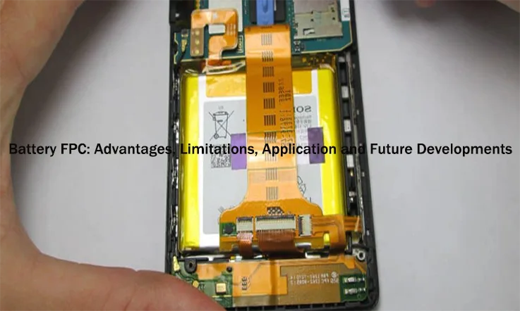
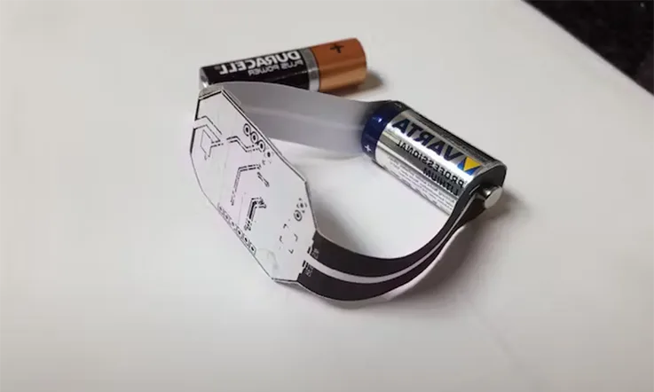
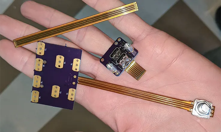
What is a Battery FPC?
Battery FPC, the abbreviation for Battery Flexible Printed Circuit, it is a flexible electronic circuit utilized for linking a battery to the accompanying electronic elements within an apparatus. The design philosophy behind the Battery FPC incorporates thinness, lightness and flexibility, typically making it a perfect fit for devices demanding a compact yet resilient source of power.
Unlike traditional rigid circuit boards, Battery FPC can be bent and curved to fit into tight spaces. This characteristic is vital for devices of unconventional shapes or dimensions. Furthermore, Battery FPC can be specifically tailored to address the explicit requirements of a particular device, allowing for greater design flexibility and improved performance.
What is FPC?
FPC stands for Flexible Printed Circuit. This denotes an electronic circuit constructed from thin, flexible materials, commonly a solitary polymer film or a composite of multiple polymer film layers. FPC are strategically engineered to serve as substitutes for conventional Rigid PCB circuit boards in particular applications, where properties such as lightweight, flexibility and space conservation are requisites.
FPC are composed of conductive pathways and pads meticulously etched onto a malleable substrate’s surface, typically fashioned from polyimide or polyester. These pathways and pads form the indispensable electrical linkages between distinct electronic constituents, encompassing integrated circuits (ICs), resistors, capacitors, and LEDs.
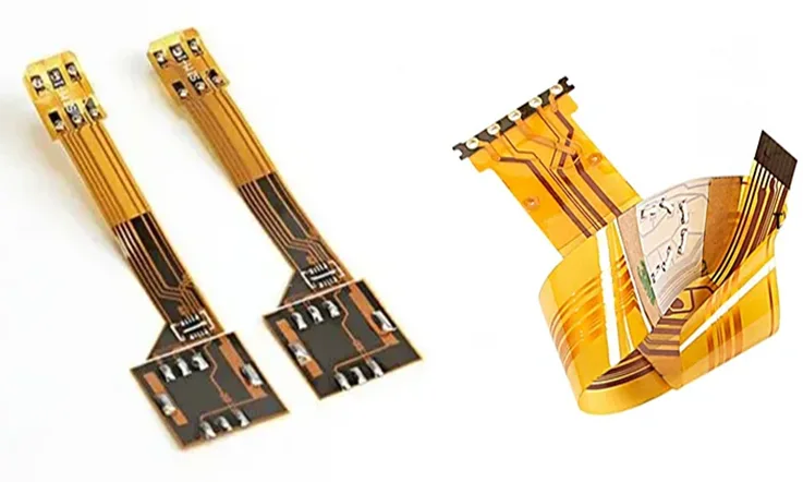
FPC can be manufactured in various shapes and sizes, depending on the requirements of the application. They may manifest as single layer, double layer and multi-layer, brandishing diverse thicknesses and copper weights. Their design can also incorporate a variety of connectors such as Zero Insertion Force (ZIF) and Flat Flexible Cable(FFC), or specific FPC connectors.
FPC are widely used in electronic devices that require flexibility, durability, and miniaturization, such as a broad spectrum of devices like smartphones, laptops, tablets, digital cameras, medical appliances, and car electronic systems. Versus standard rigid circuit boards, FPC present a comprehensive array of benefits such as notable weight diminution, superior resilience to shock and vibration, streamlined assembling and upkeep procedures, along with a heightened degree of design flexibility.
How Does Battery FPC Work?
Battery FPC works by connecting a battery to other electronic components in a device using a flexible printed circuit. Engineered for thinness, lightweight, and flexibility, the Battery FPC caters ideally to apparatuses necessitating compact and robust power solutions.
The Battery FPC consists of a thin layer of flexible substrate, such as polyimide or polyester, with conductive traces and pads etched onto its surface. These conductive routes are made from copper or comparable conductive resources, facilitating the inception of electrical connections amid the battery and ensuing electronic components integrated in the gadget.
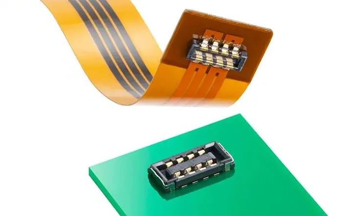
The Battery FPC is linked to the battery via a specific connector type, commonly a JST connector or an FFC/FPC connector. Possessing customizable features, the Battery FPC can be tailored to accommodate the unique requirements of the device, offering varied shapes, sizes, and thicknesses to support diverse battery dimensions and arrangements.
Upon connection of the Battery FPC to the battery, it can be unified with additional electronic constituents within the device, including microcontrollers, sensors, displays, and actuators. Category-defining characteristics of the Battery FPC, such as its ability to be contorted and curved to slot into compact zones, render it a superb choice for appliances characterized by non-standard shapes or magnitudes.
In essence, the Battery FPC functions by establishing a flexible and dependable linkage between a battery and various electronic entities within a device, allowing for greater design flexibility and improved performance.
Advantages of Battery FPC
Flexibility: Among the paramount benefits of Battery FPC is its Flexibility. It can be bent, twisted, and shaped to fit into tight spaces and conform to the shape of the device, it stands as an optimal solution for apparatuses necessitating a compact and flexible power source.
Lightweight: Battery FPC is much lighter than traditional rigid circuit boards and other types of battery connections, making it an excellent option for devices that require lightweight components, such as portable electronics and wearable devices.
Reliability: The Battery FPC is skillfully designed to deliver high reliability. It has limited connective junctures and eliminates the existence of movable components, effectively diminishing the probability of malfunction while enhancing the device’s comprehensive performance.
Enhanced Resilience to Shock and Oscillation: The Battery FPC exhibits a greater resistance to shock and vibration compared to the conventional rigid circuit boards, which are susceptible to fissures or fractures under strain. Consequently, This makes it an excellent option for devices that are subject to frequent movement or impact, such as automotive electronics and industrial equipment.
Simplified Assembly and Maintenance: The implementation of Battery FPC during the assembly process can be effortlessly achieved, curtailing both time and production costs. In addition, it can be conveniently substituted or mended if required, thus enhancing the device’s comprehensive maintenance.
Increased Design Flexibility: The Battery FPC offers customization to cater to the distinct requirements of the device, with a variety of shapes, sizes, and thicknesses available to accommodate diverse battery sizes and configurations. This yields greater design flexibility and uplifts the performance.
Limitations of Battery FPC
Production Expense: Manufacturing Battery FPC may be costlier compared to conventional rigid circuit boards, consequently raising the overall device expenditure.
Restrained Current Capacity: Battery FPC exhibits a limited current capacity, thereby implying that it might not be apt for devices demanding high power output or swift charging.
Constrained Temperature Tolerance: Battery FPC may feature a restricted temperature range that could potentially influence its performance under severe temperatures or in harsh conditions.
Finite Durability: Despite Battery FPC being sturdier than traditional rigid circuit boards, it could still succumb to wear and tear over duration, particularly in high-stress situations.
Design Intricacy: Crafting the Battery FPC is likely to be more intricate as compared to traditional rigid circuit boards, necessitating particular expertise and specific equipment for manufacturing and assembly.
Limited Compatibility: Battery FPC may not be fully compatible with all battery types or connectors, thus impeding its application in certain scenarios.
Applications of Battery FPC
Battery FPC is leveraged across an extensive array of electronic apparatuses, wherein attributes such as flexibility, light-weightedness, and economization of space are requisites. Following are some prevalent use-cases of Battery FPC:
● Portable Electronic Devices
● Healthcare Equipment
● Automobile Electronics
● Industrial equipment
● Home Electronic Products
● Defense and Space Equipment
What are the Differences Between FFC and Battery FPC?
Both FFC (Flexible Flat Cable) and Battery FPC (Flexible Printed Circuit) are types of flexible circuits implemented to create connections amongst electronic components inside a device. Nevertheless, significant distinctions exist between these two types.
Structure: FFC is characterized by a series of conductive wires that are encapsulated between two layers of pliable insulating material, forming a flat-type cable. In contrast, Battery FPC constitutes a flex PCB circuit board comprising a thin substrate layer onto which conductive paths and pads are meticulously etched.
Functionality: FFC primary role is to establish connections between electronic components within an apparatus, such as flat panel displays or touchscreens. Conversely, Battery FPC has a more specific purpose, which is to facilitate a connection between a battery and other constituent electronic components within an instrument.
Flexibility: While both FFC and Battery FPC possess flexibility, Battery FPC generally showcases greater pliability and robustness, attributed to its thin substrate material and carefully etched conductive traces.
Thickness: Conventionally, FFC exhibits a greater thickness compared to Battery FPC because of its composite layers of insulating material and conductive wires. Owing to its slimmer profile, Battery FPC becomes a preferred choice for devices with space constraints.
Connector Type: The FFC generally employs a ZIF (Zero Insertion Force) connector, whereas Battery FPC tends to utilize JST connector or standard FFC/FPC connector.
Therefore, despite the fact that both FFC and Battery FPC are types of flexible circuits utilized for the integration of electronic components within an apparatus, distinctions are evident in their fabrication, functionality, flexibility, thickness and connector style. FFC is chiefly employed for electronic component linkage, whereas Battery FPC is designed expressly for establishing a connection between a battery and other electronic components. Typically, Battery FPC exhibits superior flexibility, is thinner and features a unique connector in comparison to FFC.
Future of Battery FPC
The outlook for Battery FPC appears to be vibrant, with ongoing evolvement and advancements in the sphere of pliable electronics. Allow me to present some prospective progressions for Battery FPC:
1. Increased Power Capacity: One crucial arena of consideration for Battery FPC is augmenting its power holding capability, fulfilling the rising requirement for devices with robust power. This could involve using new materials or developing new manufacturing processes to improve the conductivity and current-carrying capacity of Battery FPC.
2. Improved Durability: Another area of focus for Battery FPC is improving its durability and resistance to wear and tear. This could involve the generation of new materials or coverings that provide superior shielding from environmental elements like moisture, heat, and UV radiation.
3. Integration with Other Flexible Electronics: Battery FPC could feasibly amalgamate with diverse types of flexible electronics, including sensors, displays, and memory equipment, giving rise to entirely flexible systems. This could pave the way to unparalleled possibilities in wearable technology, medical implants, and an expanse of other applications.
4. Development of New Applications: Pursuant to the ongoing evolution of Battery FPC technology, the emergence of new applications and markets is quite probable. To illustrate, Battery FPC could find usage in the formulation of robotics, intelligent fabrics, or flexible solar cells.
5. Increased Manufacturing Efficiency: The development of new manufacturing processes and materials could improve the efficiency and cost-effectiveness of producing Battery FPC. This could make it more accessible to a wider range of industries and applications.
In summary, the future of Battery FPC looks bright, with potential for increased power capacity, improved durability, integration with other flexible electronics, development of new applications, and increased manufacturing efficiency. Such advancements could serve as catalysts for innovation and expansion across various sectors, thereby reinforcing the position of Battery FPC as a crucial element in the future landscape of flexible electronics.
Conclusion
Battery FPC is a type of flexible printed circuit, is specifically engineered to establish a connection between a battery and other electronic elements within a device. Compared to conventional rigid circuit boards, Battery FPC offer many benefits. These include its flexibility, capability for space optimization, elevated reliability, customizability, decreased assembly duration and costs and enhanced performance. Battery FPC finds a spectrum of uses in numerous electronic devices, spanning everything from handheld electronics and medical equipment to automotive and industrial applications.
While Battery FPC has some limitations, including cost and limited current capacity, its potential for increased power capacity, improved durability, integration with other flexible electronics, development of new applications, and increased manufacturing efficiency make it an essential component in the future of flexible electronics.
With the relentless progression of technology and the advent of novel applications for flexible electronics, Battery FPC is poised to assume a progressively significant function in energizing future devices and systems. Its inherent flexibility, durability and customization capabilities render it a supremely fitting solution for a multitude of applications. Furthermore, its capacity for innovation and growth puts it in the spotlight as a fascinating field to monitor closely.
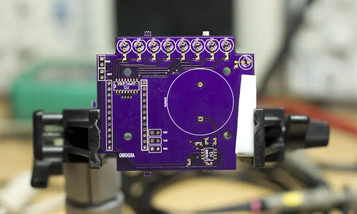
The advancement of mobile electronic components has been nothing short of revolutionary. While the fabrication of miniature, smart electronic instruments can prove intricate, the utilization of versatile printed circuit boards has streamlined the production of complex electronic elements.
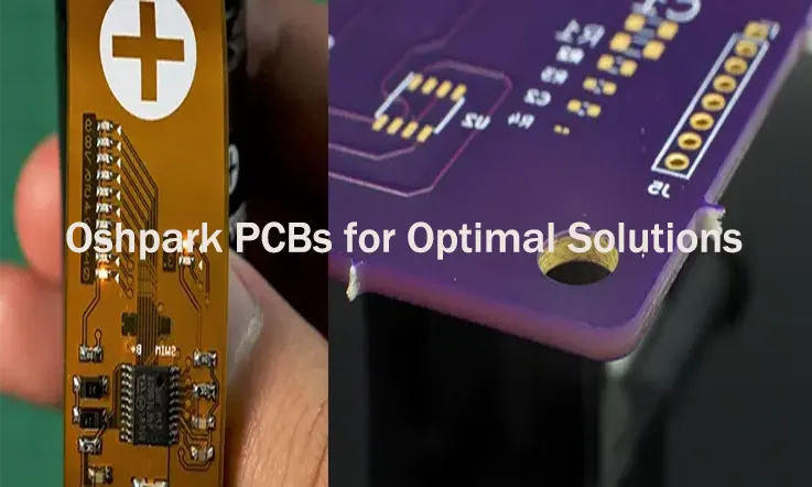
Flex PCB have proven to be particularly efficient in static and dynamic electronic devices, and as a result, many industries are incorporating them in the production of portable multi-functional devices. OSHPARK, a respected producer of flex PCBs, has solidified its standing for top-notch quality in the sector. In this piece, we’ll explore further into OSHPARK and their flex PCB.
What is OSHPARK?
OSHPARK is a well-regarded online platform providing fabrication and assembly services for printed circuit boards. It is a community-driven platform that enables hobbyists, makers, and engineers to design and order custom PCBs in small quantities at an affordable cost. OSHPARK PCB, known for their distinctive purple-hued boards, have become a brand hallmark. The venture took off in 2011, and has since earned commendation for top-tier PCB provision with rapid delivery times. Broadly utilized within the electronics industry, OSHPARK PCB are first choice for prototype creation and limited-scale production of electronic apparatus.
History and Background of OSHPARK
OSHPARK was founded in 2011 by Drew Fustini, Laen O’Connor and Dave Young. The company was born out of frustration with the high costs and long lead times associated with low-volume PCB production. the founders hope to devise a service enabling enthusiasts, inventors, and engineers to avail high-quality PCBs in smaller volumes at economical pricing.
The company’s name, “OSHPARK,” is a combination of “OSH” (short for “Open Source Hardware”) and “park” ( signify a community space). The founders of company believed that open-source hardware was a crucial part of the maker movement and wanted to create a platform that would support and encourage its development.
OSHPARK quickly garnered popularity within the creator community, recognized for their notable purple-hued circuit boards. The firm’s dedication to superior quality and exceptional customer service secured its differentiating space amidst widespread competition. Consequently, it has emerged as one of the most sought-after PCB fabrication services on the digital platform.
In 2018, OSHPARK was acquired by Advanced Circuits, a leading PCB manufacturer, but it continues to operate as an independent brand with its own unique identity and community.
Oshpark’s Technologies and Integrations
OSHPARK PCB sets the industry standard as a premier fabricator of top-tier flex PCB. It is distinguished for its superior technologies and synergies that facilitate meeting the stringent industry benchmarks for PCB production. One of the technologies that OSHPARK utilizes in its PCB production is the advanced computer-aided design (CAD) software. This proprietary software empowers the firm to generate exact and intricate designs in accordance with specific client stipulations.
OSHPARK PCB also employs advanced printing technologies to produce PCB with high resolution and accuracy. The company’s printing equipment uses advanced techniques such as laser direct imaging and inkjet printing to achieve high-quality results. OSHPARK’s printing technologies are highly efficient, producing PCB with excellent resolution and reduced manufacturing times.
Moreover, OSHPARK PCB amalgamates cutting-edge technologies in PCB examination and analysis. The firm leverages automated optical inspection (AOI) along with X-ray scrutiny to assure that each PCB is congruent with the stipulated quality benchmarks. These contemporary technologies facilitate OSHPARK in detecting and rectifying any discrepancies or imperfections in the PCB prior to their dispatch to the clientele.
OSHPARK PCB’s technologies and integration are designed to ensure that their PCB meet the highest industry standards. The company’s commitment to quality has earned it a reputation as a leading manufacturer of high-quality flex PCB.
Oshpark Flex PCB Types
Providing a comprehensive array of flex PCB types, OSHPARK caters to the extensive gamut of its client’s requirements. The offerings encompass the following types of flex PCB:
Single layer flex PCB: Incorporating a solitary conductive layer, these flexible PCB are distinguished by their simplicity. Their rudimentary design lends itself seamlessly to applications requiring a flexible and uncomplicated circuit layout.
Double sided flex PCB: Furnishing two conductive layers, these flex PCB offer enhanced design adaptability. Their dual-layer structure suits applications that demand a higher level of complexity.
In addition, the following are the minimum design rules for two-layer flex PCB:
● 6mil (0.1524mm): specified as the trace width.
● 5mil (0.127mm): denoted as the annular ring dimension.
● 6mil (0.1524mm): signified as the trace clearance.
● 10mil (0.254mm): characterized as the drill size.
Multi-layer flex PCB: These flexible PCB are characterized by three or more layers of conductive matter. The high-density circuit requisites of certain applications make multi-layer flex PCB an optimal choice.
the following are the minimum design rules for 4-layer flex PCB:
● 5mil (0.127mm): The prescribed measure for the trace width.
● 4mil (0.1016mm): The exact specification for the annular ring.
● 5mil (0.127mm): Designated value for the trace clearance.
● 10mil (0.254mm): Officially recognized standard for the drill size.
the following are the minimum design rules for 6 layer flex PCB:
● 5mil (0.127mm): Trace width is designated as such.
● 4mil (0.1016mm): This marks the annular ring‘s standard dimension.
● 8mil (0.2032mm): The drill size is defined by this measure.
● 5mil (0.127mm): This signifies the trace clearance for the design.
Rigid-flex PCB: These PCB exhibit a hybrid nature with sections both rigid and flexible. By amalgamating the advantages of both types of circuitry, rigid-flex PCB cater perfectly to applications that demand a synthesis of the two.
Sculptured flex PCB: These are flexible PCB with a unique three-dimensional shape. Sculptured flex PCB are ideal for applications that require a customized shape or fit.
OSHPARK’s range of flex PCB types allows clients to choose the type of PCB that best suits their specific application requirements.
Bend Radius of OSHPARKFlex PCB
Determination of the bend radius for a flex PCB, either in a static or dynamic state, is dependent on the thickness of all the layers present in the board that are affected by bending. This assessment is done by multiplying the board’s thickness by the bend ratio. A static bend is a process where the flex PCB is manipulated into a specific shape and subsequently installed while maintaining this curvature.
Contrastingly, a dynamic bend signifies the bending and straightening progression which a flex PCB experiences. Determining the bend radius for a dynamic bend may pose certain challenges, yet maintaining larger dynamic bends is essential to reduce wear during functionality. Conversely, brisk, dynamic bends could precipitate rapid PCB degradation.
Quality Assurance of OSHPARK
OSHPARK has a strong commitment to quality assurance and takes several steps to ensure that its PCB meet the required specifications and perform reliably.
Design verification: Before manufacturing begins, OSHPARK verifies the design files to ensure that they are error-free and meet the required specifications.
Material selection: OSHPARK uses high-quality materials, including FR-4 fiberglass, copper foil, and solder mask, to ensure that its PCB meet industry standards and perform reliably.
Testing: Every PCB undergoes electrical connectivity and functionality tests prior to distribution. OSHPARK utilizes state-of-the-art automated testing machinery to verify that every board adheres to the necessary specifications.
Quality control: OSHPARK benefits from a cadre of seasoned technicians who carry out meticulous visual assessments and manual analysis, ensuring that each fabricated PCB satisfies the required specifications.
Client feedback: OSHPARK greatly appreciates customer suggestions and employs them for the enhancement of its product offerings and services. The firm boasts a robust assembly of product creators and engineers who contribute their designs and cooperate on endeavors, providing invaluable feedback and discernment.
Customer Support and Community
OSHPARK exhibits a profound commitment towards customer service and community engagement, which has been instrumental in establishing a steadfast clientele comprising hobbyists, makers, and engineers. The following are some of the features provided by OSHPARK related to customer support and community interaction:
Online support: OSHPARK offers online support through its website, including a knowledge base, FAQs, and detailed instructions for designing and ordering PCB.
Community Forum: OSHPARK boasts a vibrant community forum that provides a platform for clients to showcase their designs, solicit feedback, and team up on ventures. The forum, overseen by OSHPARK personnel, constitutes a stellar resource for knowledge acquisition and professional networking.
Social media: OSHPARK commands a robust presence on various social media platforms – Twitter, Facebook, and Instagram included. These platforms serve as effective channels to broadcast novel developments and news pertinent to its offerings and services.
Customer Service: OSHPARK employs a committed customer service unit, accessible to resolve queries and extend support through email. Additionally, the company also possesses a direct contact number for addressing urgent matters.
Blog: OSHPARK has a blog where it shares news and updates about the company, and providing instructive and resources beneficial to creators and engineers.
Conclusion
OSHPARK PCB has become a popular choice for hobbyists, electronics manufacturers, and engineers looking for high-quality PCB in small quantities. Through their commitment, to quality, affordability and customer care OSHPARK has built a following and established itself as one of the premier online PCB fabrication services.
OSHPARK PCB is likely to continue to innovate and expand its offerings to meet the evolving needs of its customers. The company may investigate fresh fabrication methodologies, materials, and design instruments to make PCB fabrication increasingly obtainable and economical for hobbyists and creators.
OSHPARK’s strong community and online presence are also likely to play an important role in its future growth. With the continuous development and evolution of the maker movement, OSHPARK is strategically poised to be a significant participant in this vibrant and stimulating community.
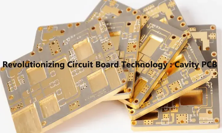
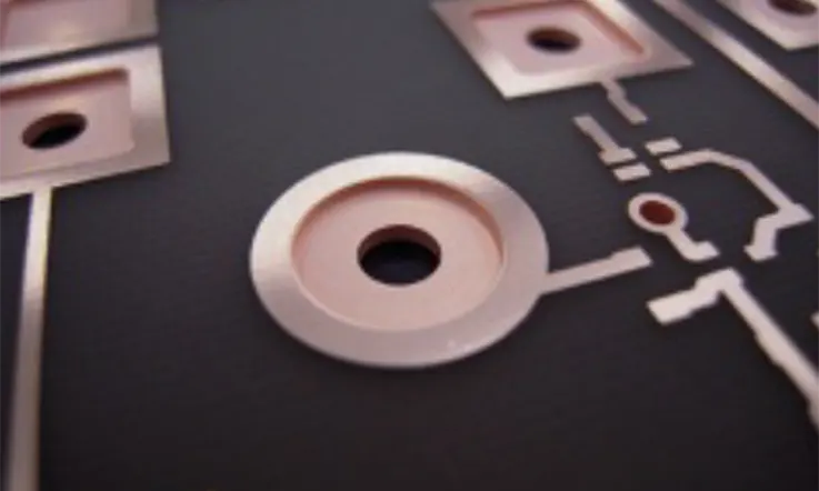
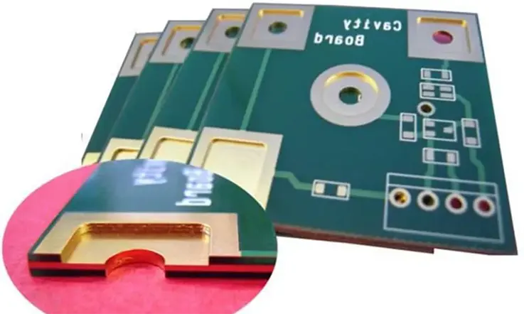
PCB incorporate various technologies to enhance their performance, and one such strategy is the implementation of cavity PCB. Cavity PCB feature indentations or hollowed areas on the board, which serve to ensure precise dimensions and accuracy.
Employing cavities in PCB provides multiple benefits, particularly in relation to component positioning and assembly. By incorporating these indentations, the component incorporating these indentation becomes more streamlined and efficient. Moreover, the assembly procedure is uncomplicatedly streamlined, promoting increased productivity efficiency.
Should you possess any queries pertaining to cavity PCB, rest assured you have arrived at an apt platform. In this post, we will address several fundamental questions, providing you with a comprehensive understanding of PCB cavities. The perusal of this article, you can expect your queries concerning cavity PCB to be thoroughly answered.
What is Cavity PCB?
Printed circuit board, or PCB, function as the core substrate for electrical constituents and facilitate the creation of specific electrical functions across a vast spectrum of electronic apparatuses.
In most cases, PCB consist of multiple layers that need to be interconnected to ensure their functionality. One methodology to actualize this involves the assimilation of cavities on the PCB – these constitute perforations or apertures executed to facilitate the connection of these strata.
To create cavities, holes are typically drilled through the outer copper layer of the PCB and extend into the inner layers, stopping short of penetrating all layers of the board.
Cavities primarily serve to reduce the overall height of the components they surround. Their purpose is to enhance the clearance between components on the board.
Considering the current focus on downsizing components and devices, cavities hold significant importance in PCB. They play a crucial role in accommodating the shrinking dimensions and improving the overall performance of electronic systems.
Types of Cavity PCB
Various electronic applications often utilize a range of cavity PCB. Among the frequently used types are:
Through-Hole Cavity PCB: Varieties of cavity PCB falling into this category bear cavities drilled with through-hole via that establish a connection between the top and bottom layers of the board. The via are pierced through the entire board, then plated to yield electrical conductivity.
Blind Via Cavity PCB: Cavity PCB of this type feature cavities equipped with blind via that bind the top and interior layers of the board. The via are drilled only partially through the board, and then plated to provide electrical conductivity.
Buried Via Cavity PCB: These cavity PCB exhibit cavities boasting buried via connecting the inner layers of the board. Such via are drilled and plated prior to the layer lamination process, rendering them less discernible on the board’s surface.
Stacked Via Cavity PCB: In this type of cavity PCB, cavities possess stacked via that link numerous inner layers of the board. These via are drilled and plated in a sequential manner, which enables reducing the overall dimensions of the board while boosting the layer count.
Metal Core Cavity PCB: This types of cavity PCB incorporate a metallic core stratum intermediate to the top and bottom layers of the board. This metal core amplifies thermal conductivity, thus making these PCB types an optimal fit for high-power demanding applications.
These are just a few examples of the types of cavity PCB that are available. The types of cavity PCB utilized is contingent upon the necessities of the particular use-case. Including factors such as: size and shape of the cavity, layer count necessary and the desired electrical and thermal properties.
Construction of the Cavity PCB
Cavity PCBs offer additional functionality compared to standard PCBs due to their structural recesses. One notable advantage is the ability to incorporate heat sinks called “coins,” which are inserted into the cavities. These coins facilitate the positioning of electronic components below the surface, resulting in a slimmer overall profile for the assembled printed circuit board.
Moreover, the inner surfaces of the cavities can be utilized for electrical contacts, typically for grounding purposes. While there are various methods to create a cavity in a printed circuit board, the most common approach involves mechanical removal of material from the PCB structure to form window-shaped recesses in multilayer PCBs.
During the assembly of prepreg and laminate materials, these layers form the walls of the cavities. In situations where the cavity functions as a microwave/RF resonant cavity, the frequency is determined by the cavity’s size, and it is crucial for the PCB manufacturer to control the X, Y, and Z dimensions of the cavity. The cavity designs can be implemented in multiple locations on a single PCB, with different depths, and can even be edge plated if required.
Design Considerations for Cavity PCB
When creating a cavity PCB it’s crucial to consider important factors to guarantee the board operates as planned. Some key things to think about when designing a cavity PCB are:
Cavity size and shape: The size and shape of the cavity will depend on the specific application requirements. The cavity ought to be of sufficient dimension to house the components and requisite structures, yet simultaneously adhering to the confinements of the board’s size and thickness.
Cavity placement: The position of the cavity on the board also hinges on the application directives. The cavity must be strategically situated to facilitate optimum thermal dissipation and electrical connectivity.
Component placement: The strategic arrangement of components within the cavity warrants meticulous consideration to ascertain their appropriate mounting and secure fixture. The components should be positioned such that they do not interfere with each other or with the surrounding structures.
Signal integrity: The design must integrate potential implications of the cavity on the board’s electrical attributes. Trace placement and routing must be performed with caution to avert any interference or depreciation of signal strength.
Thermal management: Cavity PCB may have increased thermal management requirements due to the cavity’s presence. The board’s thermal characteristics must be analyzed meticulously ensuring efficient heat diffusion, thereby averting possible component damage.
Board thickness: The thickness of the board inherently influences the feasible cavity size, along with the aggregate mechanical characteristics of the board. Board thickness determination must involve sound judgement, aligned with the specific application requirements.
Fabrication Considerations: The design must incorporate the manufacturing protocol for cavity PCB, encompassing any limitations or prerequisites for drilling, plating vias, laminated layers, or implementing surface finishes.
How to Make Cavity in PCB?
The creat of a cavity in a PCB entails the elimination of a segment of the board material, to generate a recessed area. This done for a variety of reasons. Such as: provide space for a component that needs to align perfectly with the board surface or to furnish a specified space for a battery or different component.
Here are the general steps to make a cavity in a PCB:
Ascertain the position and magnitude of the cavity: Pinpoint the desired location of the cavity on the PCB and establish its required dimensions. These factors will aid in the selection of fitting cutting tools and techniques.
Design the cavity in your PCB software: Use your PCB design software to create a cavity layout. This can be done by creating a new layer in your PCB design and drawing the cavity shape using the appropriate tools.
Generate a tool path: After designing the cavity, generate a tool path for your CNC machine. The tool path will guide the machine to cut out the cavity in the PCB.
Select an appropriate cutting tool: Opt for the cutting tool that aligns with the dimensions and form of the cavity. The utilization of either a milling cutter or a routing bit, contingent upon the size and geometry of the cavity, is advisable.
Set up the CNC device: Set up CNC apparatus and install the selected cutting tool.
Execute the cavity cut: Operate the CNC machinery to carve out the cavity within the Printed Circuit Board (PCB). Adherence to safety protocols is imperative and observing the cutting procedure is crucial to guarantee everything is progressing according to the plan.
Clean up the PCB: After cutting the cavity, clean up the PCB to remove any debris or residue left behind.
What are the Materials Used in Cavity PCB?
The materials used in creating a cavity in a printed circuit board can vary depending on the specific application and requirements. Nevertheless, certain frequently employed materials in cavity PCB encompass.
FR-4: This frequently utilized PCB material is crafted from a fabric of woven fiberglass steeped in epoxy resin. It offers a budget-friendly alternative and aligns well with the majority of applications.
Rogers: This superior-performance PCB material is typically employed in high-frequency and microwave applications. It possesses a low dielectric constant and reduced loss tangent, rendering it exceptionally suitable for high-velocity signal transmission.
Aluminum: This material is frequently engaged for the purpose of heat dissipation in PCBs. It is a proficient conductor of heat and is conventionally employed in LED lighting applications.
Copper: This prevalent PCB material is utilized extensively within the conductive strata of the boards. With its superlative conductive properties, it is employed to fabricate traces and pads for efficient electrical conduction.
Ceramic: Ceramic constituents are frequently employed in high-power applications, attributed to their extraordinary thermal conductivity and robust resistance to elevated temperatures.
Teflon: This high-performance substance is commonly harnessed in microwave and RF applications. Owing to its minimal dielectric constant and loss tangent, Teflon proves to be ideal for high-frequency signal propagation.
The choice of material for a cavity PCB depends on various factors such as the application’s requirements, performance, and cost. It is imperative to opt for the pertinent material tailored to the specific application to guarantee dependable and efficient performance.
Comparison between Cavity PCB and Other PCB Types
Cavity PCB confer exclusive merits that set them apart from the general spectrum of PCBs. However, they also come with their unique constraints and trade-offs to mull over while selecting a PCB aligned with a specific application. Here is a comparative analysis between cavity PCBs and other prevalent PCB types:
Cavity PCB vis-a-vis Single-Sided PCB:Cavity PCB typically have higher manufacturing costs than single-sided PCB, due to the additional layer(s) and the cavity structure. Furthermore, they can host more sophisticated circuitry and components.
Cavity PCB against Double-Sided PCB:Cavity PCB, along similar lines, generally carry elevated manufacturing expenses compared to double-sided PCB, owing to the same factors cited above. However, cavity PCB can provide better electrical performance and can reduce the overall size and weight of the board.
Cavity PCB in comparison with Multi-layer PCB: Cavity PCB can analytically be classified as a types of the multilayer PCB, distinguished specifically by their unique cavity architecture. They can bestow enhanced thermal capabilities and facilitate overall board dimension and weight reduction, albeit potentially at a higher production cost compared to certain multilayer PCB.
Cavity PCB over Flex PCB: Characteristically, cavity PCB exhibit greater rigidity compared to flex PCB, which may restrict their utility in specific applications that necessitate flexibility. Despite flex PCB possibly entailing higher manufacturing expenses, they bestow enhanced design versatility and find applicability in scenarios characterized by constricted space.
Cavity PCB versus Metal Core PCB: Cavity PCB and metal core PCB are both designed for high-power applications, but with different approaches. The former leverages a cavity design to impart superior thermal expulsion, whilst the latter utilizes a metallic core stratum to bolster thermal conduction. Both PCB types present commendable thermal behavior, however, the selection is contingent on the distinct necessities of the application at hand.
In the end, opting between cavity PCB and other PCB types will depend on the specific requirements of the application. This encompasses elements like dimensions, weight, thermal attributes, electrical performance and cost considerations.
How to Choose the Most Reliable Cavity PCB Manufacturer?
The selection of an appropriate cavity PCB manufacturer is paramount in receiving a premium product satisfying your unique requirements. Here are several integral elements to deliberate when zeroing in on a trustworthy cavity PCB manufacturer:
Experience and expertise: Look for a manufacturer that has extensive experience in producing cavity PCB and has a proven track record of delivering high-quality products. Ascertain if they’ve had experience in producing PCB compatible with your specific application.
Production Proficiency: Ascertain that the manufacturer possesses the requisite machinery, operations, and facilities for fabricating cavity PCBs to your precise specifications. Gather information about their production abilities, inclusive of the of materials and processes they use.
Quality Assurance: A dependable cavity PCB manufacturer must establish stringent quality assurance protocols to guarantee that every board aligns with the mandated specifications. Inquire about their quality assurance measures, testing methodologies, and official certifications.
Customer service: Look for a manufacturer that provides excellent customer service and responds promptly to your inquiries and concerns. They should be willing to work closely you, comprehend your unique prerequisites and offer tailor-made solutions as necessary.
Budget Considerations: While financial outlay is indeed a critical element, it shouldn’t be the solitary criterion when deciding on a cavity PCB manufacturer. Seek a manufacturer who not only presents competitive pricing but is also proficient in delivering top-tier products alongside superior customer service.
References and reviews: Check for references and reviews from other customers to get a sense of the manufacturer’s reputation and track record. Consider feedback concerning the superior quality of their PCB board, the level of client service, and overall dependability.
By taking these elements into account, one can opt for a dependable cavity PCB manufacturer that aligns with your particular necessities and provides superior quality products either meeting or surpassing your anticipations.
Applications of Cavity PCB
Cavity Printed Circuit Boards are incorporated across a myriad of industries including, but not limited to, automotive, aerospace, medical, and telecommunications sectors. Some of the recurrent applications of cavity PCB encompass:
●Power electronics
●RF/microwave applications
●LED lighting
●Medical devices
●Automotive
●Aerospace
This is just a snapshot of the numerous instances where Cavity Printed Circuit Boards find their usage. The distinctive application is contingent on the unique system or device prerequisites, but cavity PCB present an abundance of advantages such as improved thermal management, size reduction and superior signal quality.
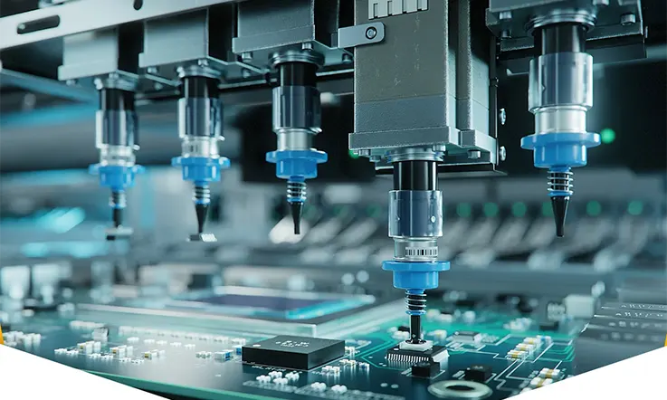
What are the Cavity PCB Components Assemble Technologies?
Implementing component assembly on cavity PCBs can engage a diversity of technologies and techniques, contingent on the distinct stipulations of the board and its application. Here are several of the prevalent technologies applied in cavity PCB component assembly:
Surface Mount Technology (SMT):
Surface-mount technology is a ubiquitous method employed in the assembly of components on cavity PCBs. With SMT, components are affixed directly onto the surface of the board. The attachment is executed by utilizing solder paste, followed by a reflow oven to secure the components to the board.
Through-hole Technology:
Through-hole technology encapsulates the practice of perforating component leads or pins through apertures in the board, succeeding which they are soldered to the contra side. This method, though not as frequently employed for cavity PCBs, might be requisite for specific applications or components.
Flip-chip Technology:
Flip-chip technology encompasses the procedure of affixing components directly to the board’s surface, with the contact pads oriented downward. Such a technique can result in enhanced electrical performance and thermal control, albeit necessitating specialized machinery and skillset.
Wire Bonding:
Wire bonding represents the technique of utilizing a thin wire to establish a connection between the component and the board via a bonding pad. This practice is predominantly leveraged for linking integrated circuits (ICs) and other miniature components.
Die Attach:
Die attach methodology entails mounting an unencased semiconductor die directly onto the board deploying a specialized adhesive. This tack is frequently adopted for high-power and high-frequency applications, in scenarios where a packaged component could potentially engender unfavorable parasitic phenomena.
Consequently, the selection of component assembly methodology for cavity PCBs hinges upon the specific requirements of both the board and its application. Accordingly, the manufacturer has to meticulously assess the design and materials that constitute the board to ascertain the most suitable assembly technology.
What is Cavity PCB Edge Plating?
Edge plating in cavity PCB involves a plating method where a metal layer is added to the exposed edges of the cavity on a printed circuit board. The main goal of edge plating is to enhance electrical connectivity, between the board layers and enhance themechanical stability of the board.
In a cavity PCB, the cavity is generally formed by eliminating a section of the board’s material, leaving to the exposure of the cavity’s edges. These edges can subsequently be coated with a slender layer of metal, which could be copper or gold employing potential techniques like electroplating or other comparable plating methods.
The process of edge plating offers advantages for cavity PCBs, such as:
●Improved electrical connectivity
●Increased mechanical stability
●Enhanced thermal management
Cavity PCB edge plating is a specialized process that requires careful attention to detail and precise control of the plating parameters. Despite these complexities, when performed accurately, this process can offer substantial advantages pertaining to the efficiency and dependability of cavity PCB.
Is Laser Technology Applicable for Cavity PCB?
In fact, laser technology finds wide application in the production process of cavity PCB. It can serve manifold purposes in the manufacture of cavity PCB, such as perforating holes or vias, fashioning circuit patterns, and extracting surplus material near the cavity.
Laser drilling is a prevalent technique for via creation in cavity PCB, permitting the precise drilling of minute holes swiftly and accurately. This method can be particularly efficacious in the creation of blind or buried vias to establish a connection with the board’s inner layers.
Laser cutting is a tool that can be employed to creating intricate circuit patterns, which can help to reduce the board’s overall size and weight. This can be particularly beneficial in applications where compactness is essential, like in mobile devices or wearable tech.
Furthermore, laser technology may also be used for excess material elimination around the cavity, improve thermal dissipation and mitigating the risk of component breakdown due to overheating.
In conclusion, laser technology can serve as a valuable tool in the manufacturing progression of cavity PCB, offering heightened precision, speed and flexibility in the fabrication process.
Future Developments and trends in Cavity PCB Technology
Cavity PCB techniques are ceaselessly advancing to meet the needs of contemporary electronics. Following are the anticipated advancements and directions in the domain of cavity PCBs:
The rise in 3D printing; It’s clear that more and more people are turning to printing for creating cavity PCB. As a result 3D printing is gaining traction as a favored method, for manufacturing cavity PCB.
Miniaturization: An escalating demand for tinier and more compact electronic gadgets is propelling the trend towards the diminution of cavity PCB. This trend is anticipated to persist, giving rise to even more intricate and condensed cavity structures.
Collaboration with emerging technologies: Cavity PCB are predicted to amalgamate more tightly with other progressive technologies, including artificial intelligence, Internet of Things, and 5G networks. This integration is forecasted to expedite the creation of novel applications and utilization instances for cavity PCB.
Higher operating frequencies: With the incessant expansion of demand for speedier and more efficient electronic gadgets, the necessity for cavity PCB to function at escalated frequencies becomes increasingly paramount. This will necessitate the genesis of development materials and fabrication techniques to support these higher frequencies.
Improved thermal management: Thermal management serves as an essential element influencing the functionality and dependability of cavity PCB. There is an unbroken investigation towards employing new materials and configurations to enhance thermal dispersal and curtail the probability of superheating.
Eco-technology: A burgeoning requirement for ecologically considerate electronic apparatus is fueling the progression of cavity PCB, incorporating sustainable materials and production methodologies.
Thus, the outlook for cavity PCB technology is promising, contemplating enduring innovation and progression anticipated to propel new applications and instances of usage for these particularized PCB.
In a Word
Cavity PCB distinguish themselves as a specific types of printed circuit boards that incorporate a cavity construct within the board. This cavity framework optimizes thermal dissemination, cuts down on size and weight, and improved signal quality, marking them optimal for a wide array of uses across multiple sectors.
When designing a cavity PCB it’s important to take into account factors such as the cavitys size and shape component placement, signal integrity, thermal considerations and manufacturing requirements. Cavity PCB are compared to types of PCB, like single layer, double layer and multi layer boards based on the specific needs of the application.
The onward trajectory of cavity PCB technology is forecasted to experience incessant advancements and evolution, with trends tilting towards compactness, elevated operating frequencies, improved thermal management, and amalgamation with other burgeoning technologies.
Consequently, cavity PCB extend distinctive merits and gains that render them a compelling choice for an extensive range of uses in diverse sectors.
Over the past few years, the field of PCB development has witnessed significant advancements. From traditional boards for basic component integration, we have now moved towards circuit boards with complex components.
As PCB designers and manufacturers, we continuously strive to overcome challenges and achieve superior outcomes. Our goal is to provide innovative solutions and breakthroughs for various problems. In certain cases, these challenges may necessitate the development of new functionalities. This could involve a decision between a module-based or custom PCB design. In all such instances, specialized PCB types become indispensable. The ever-increasing demand to incorporate high-speed or high-power electronic capabilities into unconventional spaces has made special circuit board types crucial.
It is natural to have concerns and reservations when it comes to these specialized PCB. However, the success of PCB assembly and fabrication ultimately hinges on collaborating with the right contract manufacturer. To gain a comprehensive understanding of what constitutes a special PCB, it is essential to first define PCB board based on their mechanical and electrical properties. This knowledge will enable you to accurately define your board requirements. Additionally, we will explore how the manufacturing process of printed circuit boards using special materials can impact turnaround time and cost.
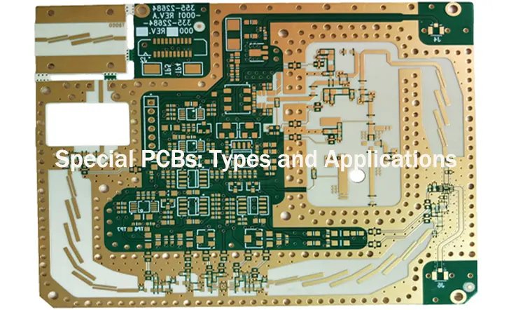
What is a Special PCB?
A Special PCB, alternatively referred to as a specialized or bespoke PCB (Printed Circuit Board), pertains to a category of circuit boards engineered and produced precisely for certain applications or requirements exceeding the usual PCB formats. These distinct PCBs are customized to accommodate the singular demands of specific trades, technologies, or environmental circumstances.
In contrast to conventional PCBs often found in diverse electronic gadgets, special PCBs are meticulously designed to tackle particular challenge or offer superior functionality. They might use advanced materials, boundary-pushing designs, or unconventional features to boost performance, dependability, or the alignment with specific components.
Special PCBs could come in multiple types like flexible PCB, rigid-flex PCB, high-density interconnect (HDI) PCB, metal core PCB, High TG PCBs, among others. Each special PCB types fulfills a dedicated function and finds its usage in precise scenarios where the conventional PCBs might not prove adequate.
The design and manufacturing of special PCBs require expertise in understanding the specific requirements, constraints, and technical considerations of the intended application. This may involve selecting suitable materials, incorporating special signal routing techniques, implementing thermal management solutions, or ensuring compliance with industry standards and regulations.
Overall, special PCBs play a crucial role in enabling the development of advanced electronic systems, devices, and technologies that require tailored circuit board solutions to meet the demanding needs of specific industries or applications.
Special PCB Types and Application
Special PCBs include different varieties engineered to cater to distinct needs and use-cases. The following are some prevalent types of special PCBs:
Flexible PCB:
Comprised of pliable materials such as polyimide or polyester, these PCB board have the ability to bend, twist, or adapt to uneven surfaces. They are perfectly suited for applications demanding compact, lightweight and bendable circuits. Such as in wearable devices, medical apparatus and aerospace systems.
Rigid-flex PCB:
By integrating the features of both rigid and flexible PCB, these boards comprise rigid components linked by flexible circuits. This provides a flexible approach to intricate electronic assemblies. Rigid-flex PCB are commonly used in devices with folding or bending mechanisms, like smartphones, digital cameras and portable electronics.
High-Density Interconnect (HDI) PCB:
HDI PCB are designed to accommodate a high number of components and interconnections in a compact form factor. They employ sophisticated microvia technology, intricate traces and numerous layers to realize high circuit density. Predominantly, HDI PCB are found in compact electronic devices. For example smartphones, tablets and other microelectronics.
Metal Core PCB:
Metal core PCB have a layer of thermally conductive material, typically aluminum or copper, as the base layer. Their exceptional heat dispersion properties make them ideal for high-power applications which engender substantial heat, including LED lighting, power electronics and vehicle components.
High-Temperature PCB:
High-temperature PCB are designed to withstand elevated temperatures without compromising performance or reliability. They utilize specialized materials with high glass transition temperatures and low thermal expansion coefficients. These PCB are used in applications such as automotive engine control units, aerospace systems, and industrial equipment operating in harsh environments.
RF/Microwave PCB:
RF (Radio Frequency) and microwave PCB are optimized for high-frequency signal transmission and minimal signal loss. They feature specific trace geometries, controlled impedance, and low dielectric constant materials to maintain signal integrity. RF/Microwave PCB are crucial in wireless communication systems, radar systems, satellite technology and high-speed data applications.
Hybrid PCB:
Hybrid PCB combine different technologies or materials to achieve specific functionalities. For example, a hybrid PCB might integrate traditional rigid PCB sections with flexible PCB sections to combine the benefits of both. Hybrid PCB are used in applications that require a combination of rigid and flexible elements, such as automotive control systems and complex industrial machinery.
These are just a few examples of special PCB types. Depending on the specific requirements and industry, there can be additional specialized PCB variants developed to meet unique application needs.
Design Considerations for Special PCBs
Designing special PCBs requires careful consideration of various factors to ensure optimal performance and functionality. Here are some common design considerations for special PCBs:
Material Selection: Choose appropriate materials based on the specific requirements of the special PCB. Consider factors such as dielectric constant, thermal conductivity, mechanical strength, and chemical resistance. Special materials like flexible substrates, high-temperature laminates, or metal core laminates may be required for specific applications.
Thermal Management: Special PCBs often handle high-power components or operate in environments with elevated temperatures. Implement effective thermal management techniques such as heat sinks, thermal vias, and copper pours to dissipate heat and maintain proper operating temperatures.
Signal Integrity and EMI/EMC: Special PCBs may have stringent signal integrity requirements. Consider signal integrity issues such as impedance matching, controlled impedance traces, and minimizing signal reflections. Implement proper grounding techniques and utilize shielding to mitigate electromagnetic interference (EMI) and ensure electromagnetic compatibility (EMC).
High-Density Design: Special PCBs may require accommodating a high density of components and traces. Optimize component placement and routing to minimize signal crosstalk, maintain clearances, and ensure proper signal integrity. Utilize advanced design techniques like blind and buried vias, microvias, and HDI (high-density interconnect) technologies.
Mechanical Constraints: Some special PCBs may need to conform to specific mechanical requirements. Consider factors such as size and form factor, mounting or attachment mechanisms, and structural integrity. Design the PCB to withstand mechanical stresses, vibrations, and environmental conditions.
Manufacturing and Assembly Challenges: Special PCBs may involve unique manufacturing processes and assembly considerations. Collaborate closely with manufacturers to ensure the design can be feasibly manufactured. Consider factors such as fabrication capabilities, assembly techniques, and any specific design rules or constraints imposed by the manufacturing process.
Reliability and Testing: Special PCBs often require high reliability. Perform thorough design verification and testing to ensure the PCB meets the desired performance criteria. Consider environmental testing, stress testing, and any specific reliability standards applicable to the intended application.
Cost Optimization: Balance the design requirements with cost considerations. Optimize the design to minimize the overall manufacturing and assembly costs while still meeting the desired specifications and performance criteria.
It’s crucial to acknowledge that these considerations function as basic guidelines, and the specific design contemplations might fluctuate based on the kind of unique PCB and its designated utilization. Hence, seeking advice from experts or specialized PCB designers adept in the particular type of unique PCB you are handling is recommended.
How to Optimize Special PCB Board Manufacturing Process?
Optimizing the production process for distinct PCB boards calls for thorough evaluation of diverse factors to guarantee productive fabrication and premium results. Below are some suggestions to optimizethe manufacturing process:
Design for Manufacturability (DFM):
Ensure that the PCB design is optimized for manufacturability. Collaborate closely with the manufacturer during the design phase to understand their capabilities, limitations, and preferred design guidelines. Consider aspects such as panelization, component placement, trace widths, and spacing to facilitate smooth manufacturing processes.
Material Selection:
Select materials that are easily obtainable and consonant with the manufacturing process. choose for materials presenting excellent dimensional constancy, excellent thermal attributes, and desirable electrical specifications for the. Work with the manufacturer to identify the most cost-effective and efficient material options.
Efficient Panelization:
Optimize the panelization of PCBs to peak the consumption of the raw material while reducing waste. Arrange the PCBs on the panel in a way that allows for efficient assembly and reduces the number of steps required in the manufacturing process. Contemplate factors such as panel dimension, gap, fiducial markers, and tooling orifices.
Component Management:
Streamline component management processes to avoid delays and errors. Maintain accurate component libraries and ensure that the Bill of Materials (BOM) is up to date. Implement effective inventory management practices to prevent shortages or excess stock. Consider automation tools for component placement and verification to improve efficiency and accuracy.
Automated Assembly:
Utilize automated assembly processes wherever possible to improve efficiency and reduce human error. Automated processes such as pick-and-place machines, solder paste deposition, and reflow ovens can significantly speed up assembly while maintaining consistency and quality.
Quality Control and Testing:
Institute stringent quality management protocols throughout the production procedure. Perform regular inspections, testing, and verification to identify and address any manufacturing defects or issues early on. Implement statistical process control techniques to monitor and improve process performance over time.
Documentation and Communication:
Maintain clear and detailed documentation of the manufacturing process, including work instructions, process flowcharts, and quality standards. Foster effective communication channels between the design team and the manufacturing team to address any design-related issues or concerns promptly.
Continuous Improvement:
Continuously evaluate and improve the manufacturing process based on feedback, lessons learned, and industry best practices. Solicit feedback from the production crew and integrate their perspectives into forthcoming design revisions. Periodically scrutinize and refine the manufacturing methodology to bolster productivity, diminish wastage, and escalate the overall quality.
Collaboration with Manufacturing Partners:
Formulate a robust association with the PCB manufacturer, perpetuating an open channel for communication. Involve the manufacturer early in the design process to leverage their expertise and ensure that the design aligns with their manufacturing capabilities.Maintain consistent collaboration to tackle any manufacturing difficulties and challenge.
Abiding by these rules and working intimately with the PCB manufacturer will enable you to refine the special PCB board manufacturing procedure, facilitating effective production, cost reduction, and the delivery of top-tier products.
Considerations for Choosing a Manufacturer for Your Special PCB
Identifying the appropriate manufacturer for your specific PCB is instrumental to securing the successful fabrication of superior quality boards that abide by your specialized needs. Below are some factors to cater to when pinpointing a manufacturer:
Expertise and Experience: Seek out a manufacturer possessing expertise and experience in creating special PCBs. Evaluate their history and probe into their proficiency in producing PCBs akin to your explicit needs. A manufacturer fortified with specialized understanding and experience will be better prepared to tackle the unique challenge of your PCB project.
Manufacturing Capabilities: Evaluate the manufacturer’s capabilities and facilities. Consider factors such as their production capacity, equipment, and technology capabilities. Ensure that they have the necessary equipment and processes required for manufacturing your special PCB, including any specialized technologies or techniques.
Quality Control and Certifications: Quality control is crucial for special PCBs. Assess the manufacturer’s quality control processes, certifications (such as ISO 9001), and adherence to industry standards. Inquire about their inspection and testing procedures to ensure that rigorous quality checks are performed throughout the manufacturing process.
Design for Manufacturability Support: Collaborative support during the design phase is essential. Choose a manufacturer that can provide design for manufacturability (DFM) feedback and guidance. They should be able to review your design, identify any potential manufacturing issues, and suggest improvements to optimize manufacturability and avoid costly errors.
Material Selection and Sourcing: Check whether the manufacturer is equipped with a broad array of materials apt for your unique PCB. They should maintain well-founded partnerships with dependable material suppliers, guaranteeing the accessibility of superior quality materials. Inquire their material selection process and determine whether they can adapt to your particular material requisites.
Prototyping and Small Batch Production: Should your needs encompass prototyping or small scale production, verify that these services are within the manufacturer’s offerings. They ought to display the flexibility and eagerness to collaborate with you during the prototyping phase, permitting iterations and modifications prior to transitioning into full-blown production.
Supply Chain Management: Evaluate the manufacturer’s supply chain management capabilities. Consider factors such as their ability to source components, manage inventory, and handle logistics efficiently. A well-managed supply chain will help ensure timely delivery of components and minimize production delays.
Communication and Support: Effective communication and support are critical for a successful manufacturing partnership. Assess the manufacturer’s promptness, communication avenues, and their ability to offer timely progress reports of your task. Choosing for a manufacturer ready to work hand-in-hand, and is quick to address any challenges or hindrances that could surface during the manufacturing course.
Cost and Pricing: Although cost is a significant factor, it shouldn’t be the only criterion driving the decision. Assess the pricing models of various manufacturers, factoring in elements like quality, technical competence, support and added-value services. select for a manufacturer who presents a just equilibrium between cost and quality.
References and Reviews: Seek references and reviews from other customers who have worked with the manufacturer. Feedback from previous clients can provide valuable insights into their reliability, quality, and overall performance.
By carefully considering these factors and conducting thorough research, you can select a manufacturer that aligns with your specific requirements, ensuring a successful and efficient production process for your special PCBs.
Importance of Special PCBs
Special PCBs play a crucial role in various industries and applications due to their unique characteristics and tailored designs. Here are some key reasons highlighting the importance of special PCB:
Customization: Special PCBs offer customization options to meet specific requirements. They can be designed to accommodate complex circuitry, unique form factors, and specific functionality that cannot be achieved with standard PCBs. This customization allows for optimized performance and integration within the targeted application.
Enhanced Performance: Specialty PCBs are design to proffer superior functionality in comparison to typical PCBs. They can offer heightened signal integrity, cut down on noise, offer increased power endurance, and advance thermal management. These performance augmentations are of utmost importance in applications where dependability, accuracy, and efficiency are cardinal.
Harsh Environment Compatibility: Special PCBs are designed to withstand challenging environmental conditions. They can be built to resist high temperatures, extreme humidity, vibrations, shock, and exposure to chemicals or corrosive substances. Such resilience ensures the reliable operation of electronic systems in demanding industries like aerospace, automotive, and industrial automation.
Miniaturization and Integration: Many special PCB are tailored to bolster miniaturization endeavors, empowering a denser packaging of electronic elements. They facilitate the production of small-scale devices and systems whilst upholding their full capacity. This is especially prominent in industries like consumer electronics and medical appliances, where size and portability are essential.
Specialized Applications: Certain industries necessitate PCBs with unique features and functions, customized for their distinct applications. Special PCBs cater to these particular requirements, including flexible PCB for bendable or curved applications, high-frequency PCB for wireless communication structures, or high-density interconnect (HDI) PCB for environments with limited spacing. These specific applications lean on special PCBs to attain peak performance and functionality.
Reliability and Durability: Special PCB are subjected to a stringent design and testing process to guarantee top-level trustworthiness and longevity. They are assembled using advanced materials, cutting-edge fabrication techniques and rigorous quality check. This dependability is paramount in essential applications like medical instruments, aerospace systems and industrial controls, where system malfunctions could lead to disastrous outcomes.
Innovation and Advancements: Special PCB are pioneers in numerous sectors driving innovation. They facilitate the evolution of breakthrough technologies such as advanced driver assistance systems (ADAS) in the automotive industry, high-speed data dissemination in telecommunications, and scaled-down medical implants. Special PCB serve as the bedrock for technological progress, continually expanding the realm of feasibility.
Which Technologies Used in Special PCB Manufacturing?
HDI Blind Buried Hole:
Blind vias, identifiable solely on the top or bottom layers of a Printed Circuit Board (PCB), are generally created from the board’s surface. In contrast, buried vias are within the inner layers of the PCB. These via types are primarily drilled in the internal layers, which underscores their categorization as internalized circuit-board holes. The adoption of blind and buried vias has markedly elevated the quality and dimensions of High-Density Interconnect (HDI) PCBs. These vias additionally boost electromagnetic compatibility, slim down layer count, streamline PCB design, and curtail expenses.
The integration of blind buried hole technology has reached its pinnacle in FR-4 prototypes with up to 20 layers. These prototypes feature a board thickness of ≤6.0mm, and blind holes spanning stages 1 to 4, utilizing laser drilling technology.
Multi-Layer Special Stack-Up Structure:
The growing necessity for high-velocity circuits has escalated the intricacy of PCB boards. In order to curb electrical disturbances, it becomes essential to separate the power layer from the signal layer. As a result, this operation employs a multi-layered approach.
Furthermore, the stack-up structure plays a crucial role in the electromagnetic compatibility (EMC) performance of circuit boards, serving as a critical measure to reduce electromagnetic interference. When the device density is higher, the PIN density of signal networks also increases. In such cases, a special stack-up structure becomes imperative.
Impedance Control:
Characteristic impedance refers to the resistance encountered by electromagnetic waves or high-frequency signals during transmission along the signal lines of components. The PCB’s characteristic impedance value must correspond to the electronic impedance of the tail and head components to ensure proper transmission of digital signals on the circuit board.
Mismatched impedance results in signal reflection, delay, attenuation, and scattering of transmitted signal energy. Therefore, PCB designers must implement impedance control. Impedance control can be achieved in FR-4, flexible circuit boards, and rigid-flex boards, allowing for 2 to 20 layers.
Thick Copper PCB:
Thick copper PCB are a type of printed circuit board with a copper thickness of 2 oz or greater. These PCB possess properties such as corrosion resistance, low-temperature resistance, high-temperature resistance, and excellent expansion performance. These attributes contribute to increased lifespan and simplified size of electronic devices. Some PCB designers can achieve 2 to 6 layers using thick copper PCB technology, with 10 oz being the maximum copper thickness.
ENEPIG is a commonly used surface finish type in circuit boards. The ENEPIG process involves depositing nickel, palladium, and gold on the PCB surface using chemical methods. This surface finish technology is non-selective.
ENEPIG integrates a 50 nm thick palladium plating and a 10 nm thick gold plating. This integration provides anti-friction properties, corrosion resistance, and good electrical conductivity. The appearance and physical properties mentioned above can be influenced by the thickness of the copper layer. ENEPIG represents the latest surface finish technology integrated into PCB prototypes.
Electroplated Nickel Gold/Gold Finger
Electroplated nickel gold, also called electrolytic gold is a surface finishing method where gold particles are bonded to the circuit board using electroplating. It is often known as hard gold because of its excellent adhesion characteristics.
This process bolsters the resistance to wear and the hardness of the circuit board, all the while curbing the spread of copper and alternate metals. It is also compliant with the specifications for soldering and thermal bonding. The resulting coating features admirable malleability, minimal strain, and low porosity. As a result, this specific layer is extensively applied in the realm of PCB proofing.
Conclusion
Special PCB cater to unique needs, offering notable benefits across a range of industries and applications. This artcle delves into several types of these special PCB like flexible PCB, rigid-flex PCB, HDI PCB, metal core PCB, and high-temperature PCB and so on.
In the course of the design procedure, numerous critical elements have been accentuated. These encompass material choice, thermal administration, signal integrity and EMI/EMC, high-density layout, mechanical restrictions, fabrication and assembly hurdles, dependability, testing, and cost efficiency. Addressing these determinants guarantees that the specially-designed PCB satisfy the specific requirements of their intended applications.
It is important to note that designing special PCB requires expertise and collaboration between designers, manufacturers, and industry professionals to ensure successful implementation. By comprehending the singular traits, challenge, and prospects related to these specialized PCB, engineers have the capability to devise revolutionary solutions that boundaries the limits of technology and propel progressions in diverse industries.
In essence, special PCB play a crucial role in enabling advanced functionalities and meeting the evolving needs of modern industries. Amidst continuing exploration and advancements, we anticipate witnessing further advancements and applications of these distinct PCB in forthcoming times, thus contributing significantly to technological progress and innovation.
Printed circuit board, widely recognized as PCB, are pivotal parts in the electronics fabrication industry, presenting themselves in diverse dimensions and forms. While rectangular and square PCB dominate the scene, you can also find non-standard geometrical forms such as octagonal and round PCB in the marketplace.
The need for unconventional PCB shapes arises due to the requirement to fit them into specific enclosures, which is vital in achieving the intended application of the PCB. Despite being less common, round PCB are becoming increasingly demanded, mostly due to the continual advancements in technology.
What is Round PCB?
A round PCB, identifiable by its circular form, functions to establish electrical connectivity to circuits. Their usage spans across diverse gadgets, inclusive of consumer electronics and LED PCBA, and they are favored for both household and business applications. Nevertheless, their creation demands a complex routing process, which subsequently escalates their cost.
PCB manufacturers pay close attention to the fabrication process of round PCBs, as it is a complex procedure. These boards feature electronic components, traces, and varying widths and are commonly used in wearable devices. Unlike rectangular PCB, a round PCB provides ample board space, making them a preferred choice for certain applications.
Therefore, round PCBs are a valuable component in electronics manufacturing, offering unique capabilities and benefits for specific applications.
Types of Round PCB
Round circuit boards are different kinds of printed circuit boards exist, such as single sided double sided and multilayer boards. Each type has its purpose and is crafted based on the specific needs of a PCB project.
● Single Sided Round PCB:
A single-sided round PCB comes with only one conductive copper layer, establishing its place as one of the most frequently employed types of round PCB. Owing to its utilization of substrates as the main material, this PCB type finds its presence across an array of applications. With components housed on one side and conductor patterns on the opposing one, single-sided round PCB effectively cater to low-density designs.
Single-sided round PCBs stand out due to their advantage of low-cost and straightforward production process, rendering them a budget-friendly solution for electronics manufacturers. The production of this type of PCB can be successfully carried out using either through-hole technology or surface mount technology.
● Double-sided Round PCB:
Double-sided round PCBs are characterized by the presence of conductive layers on each side of the board, positioning them as a viable alternative to their single-sided counterparts. Their inherent capacities have found favor across numerous applications and for specific designs, they are deemed more advantageous than single-sided boards.
Double-sided round PCBs find wide-ranging use in diverse applications such as lighting systems, wearable technology, and consumer electronics, aptly serving as dependable, high-performing alternatives for these devices. In comparison with single-sided PCB, these double-sided round circuit boards present an enlarged board space and higher component density. As a result, they rank high as a preferred option whenever manufacturing compact devices is on the agenda.
● Multilayer Round PCB:
The design of a multilayer round PCB accommodates more than two layers of conductive materials– a feature that renders it considerably suitable for high-speed applications. The advantages of this kind of round PCB are manifold, among which an enhanced assembly density and a superior capacity stand out. These qualities make multilayer round PCB particularly fitting for scenarios where a greater board space is a necessity.
On the contrary, the manufacture of a multi layer round PCB is somewhat more intricate compared to single or double-sided PCB. The production process demands meticulous layer alignment in addition to a precise bonding of all layers so as to guarantee structural integrity. Regardless of the advanced complexities inherently associated with the making of a multilayer round PCB, their imperative role in the realm of contemporary electronics remains indubitable
Advantages of Round PCBs Over other Shapes
Here are some advantages of Round PCB over other shapes:
● Space Efficient
● Reduced EMI noise
● Better Thermal Management
● Aesthetically Pleasing
● Better Signal Integrity
Consequently, the benefits of employing round PCBs as opposed to other forms hinge upon the unique demands stipulated by a distinct application. Such needs may encompass space limitations, thermal management requirements, a necessity to reduce electromagnetic interference, or considerations of aesthetic value.
Round PCB Design
Designing a round printed circuit board can be a more intricate process compared to the typical rectangular layout due to the constraints imposed by the manufacturing process. This is majorly attributed to the constraints imposed by the manufacturing methodology. To be specific, the outer edge of a round PCB can only be formed using straight line segments. This fundamental characteristic mandates thoughtful attention and strategic planning in the preliminary design phase.
To create a circular shape for the perimeter of the board, a circle can be added to the silkscreen layer. A diverse spectrum of software instruments exists which are catered to the design of round PCBs, each harboring its own distinct set of unique features and capabilities.
It should be noted that break routing is the only separation method available for a round PCB, which further adds complexity to the design process. Consequently, a profound comprehension of the software, in conjunction with meticulous attention to the minutiae, is crucial in certifying a successful outcome.
Round Circuit Board Design Rules:
When using CAD tools to design a round printed circuit board, the first step is to draw the board’s shape in the CAD software. For high-speed appliances, a multilayered PCB is recommended, with separate layers defining the power and ground planes. A polygon editor is useful for defining the shape of these planes, and some software also allows customizing them.
Designing round circuit boards also requires panelization schemes, and break routing is a common method used for this purpose. It is crucial to maintain a minimum clearance of 10 mm between circuit boards, although this can be increased using a larger routing tool.
Eagle CAD is a widely-used software for the design of electronic circuit schematics and layouts. Circuit schematics depict how different electronic components connect, and the layout is an exact image of the circuit’s appearance on a Printed Circuit Board (PCB). By default, many designers create rectangular circuit board layouts, but Eagle CAD offers a “MITER” command that transforms the square layout into a circular one.
To employ Eagle CAD for your design, initially, you’d want to access the layout file by navigating to “File” and opting for “Open.” In scenarios where a pre-existing layout file is non-existent, there exists the possibility to originate a new file, you’d achieve this by heading to “File” and pressing “New,” then naming the file as per your requirements.
You will need to modify the board outline’s size to match the intended PCB size. The board outline typically appears as a square, and you can adjust its size by clicking on either side and dragging it left or right. Ensure that the board outline remains square, preventing it from taking an oval shape when attempting to transform it into a circle.
To actualize a circular layout, it is pivotal to align each side of the square with the circle’s diameter. Input “MITER 2” atop the layout and submit by pressing “Enter.” The icon will transition into a plus symbol. Trigger a left-click on the corner of the square, this will result in it rounding off. Should the corner appear overly diminutive, make use of “MITER 3” or above, whereas, if it’s excessively large, diminish the MITER value. This procedure needs to be replicated, bestowing the MITER command onto all corners, until the point they collectively embody a circular form.
Manufacturing Process for Round PCBs
The manufacturing process for round PCB is similar to that of other PCB shapes but has some specific steps.
● PCB Design: Utilize PCB blueprint software to develop a schematic followed by a layout of the PCB.
● Panelization: Multiple round PCBs are typically fabricated in unison on extensive panel boards, allowing for modulated manufacturing and diminished costs.
● Layer Stacking: Copper trace-filled layers are piled atop one another.
● Substrate Preparation: The PCB’s substrate material receives a coat of a photosensitive layer.
● Imaging: A photosensitive mask is generated from the layout and then implemented to expose the photosensitive layer via a process involving UV exposure and development.
● Etching: The etching phase eliminates the bare copper areas, leaving behind the final copper traces.
● Drilling: Obligatory through-holes or via holes are drilled into the PCB.
● Plating: Copper plating is supplemented to the holes and surface to establish electrical connectivity amongst the layers.
● Solder Mask Application: The solder mask substance is applied and cured to insulate the copper traces and protect them from environmental factors.
● Silk Screening: A concluding layer of ink-like substance is enforced to label the constituents and essential information.
● Final Inspection: The concluding inspection verifies that all the connections are operative, devoid of any short or open circuits, and the board conforms to the required specifications.
● Separating the PCB: The solitary PCBs are disengaged from the larger panel board, marking the cessation of the manufacturing process.
Applications of Round PCBs in Various Industries
Round circuit boards are utilized in an applications of sectors:
Consumer electronics
Automotive industry
Medical equipment
Aerospace sector
Industrial automation
Military and defense
Lighting industry
In short the adaptable nature of circular PCBs and their capacity to be accommodated in compact spaces make them a preferred option for various applications, in different industries
How to Choose the Best Round PCB Manufacturer
When it comes to the production of round PCB boards, it can be a complex process that requires careful selection of a manufacturer that delivers quality. Since Many select of manufacturers available, there are several pivotal elements to consider during decision-making. Opting for the appropriate round PCB manufacturer is vital in guaranteeing the triumphant production of top-quality products.
● Experience:
The primary criteria to contemplate when opting for a round PCB manufacturer is the eminence of the products they provide. A desirable manufacturer offers exceptional product quality whilst upholding a professional echelon of service delivery. It’s judicious to go with a manufacturer boasting profound experience in the domain as they are likely to possess the necessary proficiency for manufacturing top-tier round PCBs. One can probe into the manufacturer’s offerings and services to evaluate their appropriateness. Hence, it is crucial to carry out an exhaustive investigation and assessment prior to committing to a specific manufacturer to ensure their products and services recognize the requisite norms.
● Quality:
Round PCB manufacturers typically conduct several tests to ensure that their products meet the requisite quality for optimal performance.. The most credible manufacturers are distinguished by executing a series of quality checks on the round PCBs. Such checks may encompass the E-test, thermal stress test, microsection assessment, among other tests. Through these examinations, flaws and inadequacies on the circuit board can be promptly detected. The employment of top-notch materials in the manufacturing process is equally vital in ensuring the production of superior-quality circuit boards. A ideal manufacturer should give precedence to the utilization of prime materials to assure the prolonged lifespan and durability of the circuit boards manufactured.
● Turnaround Time:
Another critical factor when choosing a round PCB manufacturer is the consideration of turnaround time. This refers to the time frame within which a manufacturer concludes and dispatches a product to the client. It’s essential to select a manufacturer who can adhere to specific delivery schedules and ensure timely product delivery.
● Customer service:
It is worth noting that certain round PCB manufacturers are committed to supporting the research and development endeavors of their clients. These manufacturers prioritize their client’s demands by being readily available to provide exceptional service. The ideal manufacturer should be able to provide a quick response to inquiries regarding quotations, professional technical support, and customized service. It is advisable to conduct thorough research on potential manufacturers by analyzing reviews and feedback from past clients.
Why Choose JarnisTech?
● Boasting a rich tenure of over two decades in the industry, we have anchored our position as a forefront PCB fabricating corporation. Our fully-furnished infrastructures are adept at handling the most complex and detailed designs of Round PCB. Our dedication towards furnishing superior-quality products at economically viable prices has been the bedrock of our establishment’s evolution and triumph. We esteem quality and earmark the integration of state-of-the-art technology in our manufacturing operations to guarantee the conveyance of first-rate products to our clients.
● At JarnisTech, we pride ourselves on delivering reliable and high-performing Round PCB to our clients. Our products are calibrated for swift integration into devices, ensuring that they meet and exceed clients’ performance expectations. We subject all our products to rigorous E-test and functional tests, including Surface Mount Technology (SMT) application, to guarantee optimal performance.
● We understand the critical role that Round PCB play in our clients’ operations, which is why we use only standardized and high-quality PCB materials. Our raw material suppliers meet international standards, ensuring that our clients receive products that are durable and long-lasting.
● In the event of any issues, our skilled team can conduct a comprehensive 8D analysis to identify the root cause and promptly provide appropriate solutions. Our customer service representatives are fully trained to respond to clients’ queries through various communication channels and offer complete service to address all their requests.
● We are well-equipped to handle bulk orders to manage large orders from different sectors and provide a variety of PCB types such, as Embedded PCB, Laser Cut PCB, USB PCB and more. As a result our customers can anticipate their orders being safely delivered to the location promptly.
For all your Round PCB needs and other PCB requirements, please contact us today, and we will be delighted to offer our expertise.
Frequently Asked Questions
Which Type of Mounting Technology is Best for Round PCBs?
For component placement on round PCB, two techniques are at one’s disposal: Surface Mount Technology and Through Hole Technology. Among these, SMT is considered the superior choice for component placement. Being an automated process, SMT simplifies the fabrication process while boosting productivity. Furthermore, the application of SMT on round PCB mitigates stress levels, culminating in an end-product of greater quality.
How do I Panelize Round PCBs?
When panelizing round PCBs, break routing is the suggested technique. Upholding a clearance of 10mm between the round circuit boards is vital for achieving superior results, particularly when utilizing diminutive routing tools. Nevertheless, this clearance can be enlarged when employing larger routing instruments. Maintaining this clearance at a suitable degree is paramount to avoid inflicting any harm to the boards or the components during the operation.
Conclusion
The prevalence of round PCBs has escalated in multiple sectors due to their advantageous traits encompassing space-effectiveness, improved thermal management, curtailed EMI disturbances, and strengthened signal reliability. Their striking circular form also enhances the aesthetic appeal of products.
Though the manufacturing process for round PCBs is similar to other PCB shapes, special steps are executed due to their circular form.
As the ongoing inclination for device miniaturization and the escalating requirement for compact, mutually connected electronic apparatuses, the utilization of round PCB is projected to persistently grow. Technological progress within the PCB production industry, coupled with the continuous evolution of innovative design software, is also expected to augment the popularity of round PCB. Furthermore, the integration of cutting-edge materials such as high-functioning ceramics is predicted to build upon the advantages provided by round PCBs even more.
At JarnisTech, we dedicate ourselves to supply esteemed customers with premium round PCB coupled with stellar customer assistance. Our knowledgeable team is always ready to support and improve our clients’ products to meet their demanding electronics assembly needs. We present economical solutions and diligently work towards guaranteeing our patrons’ gratification. To acquire further insights on our top-tier products and services, kindly browse our website at www.jarnistech.com.
When the various components of a circuit board are subjected to tap water, it might result in short-circuits or lower the efficiency of the circuit. Thus, there’s an eminent need to shield these components from moisture and corrosion. At first, we need to must be done is to check and see if the fundamental circuitry of their device is resistant to water. In situations such as these, the adoption of waterproof PCB could be appropriatec. This guide will delve into their nature, significance, applications, and their prodution by manufacturers
What is a Waterproof PCBs?
Waterproof PCB possess a protective covering that equips them with resistance against moisture and other environmental attributes. Such PCBs are concurrently termed as waterproof printed circuit boards. This protective overlay is generally resin-based, enveloping the entire circuit board and its singular components. This fabricates a robust barricade impeding the penetration of water, dust, and other contaminants onto the board.
This waterproofing technique applies to both rigid and flexible circuit boards, offering increased safety for sensitive electronic components and electronics as a whole. It’s typical to see the implementation of waterproof printed circuit boards for critical components across diverse industries and applications. This includes realms such as medical, aerospace, military along with industrial and consumer electronics sectors
How to Waterproof Your PCB Boards?
Waterproof PCB are critically indispensable for any electronic apparatus that holds the potential to interact with water or moisture. It is possible to waterproof a printed circuit board in a variety of methods, such as the utilization of water-resistant PCB substrates, sealing of connectors, application of waterproof paint, and the deployment of waterproof material over the topmost stratum. The success of these methods can alter with varied types of PCB boards, depending primarily on the PCB’s applications and the extent of waterproofing required.
Under any and all circumstances, the optimal approach is to prevent moisture and water from reaching electronic appliances by isolating them. However, in conditions where the atmospheric water content significantly escalates, the application of waterproof PCBs is recommended for electronic circuit board usage. The PCBs employed in marine-based applications endure extremely high moisture levels throughout their operational lifespan. Consequently, standard PCBs fail to deliver effectiveness in such environments due to their propensity to absorb water.
Apply Waterproof Material on Printed Circuit Board:
This technique is utilized for the production of particularly specialized items, such as printed circuit boards for use in the control systems of vessels (ships, submarines, etc.). In this method, you can make the surface of the PCB board waterproof by adding a particular material to it, such as parylene C or parylene n.
In fact, parylene C and parylene N are the identical material. Both these substances are high-density polymers and have the potential to be morphed into exceedingly thin layers. The majority of the time, during application onto the circuit board, they exist in a liquid state. Post a specific time duration, they start the process of solidification, eventually resulting in a waterproof finish. In comparison to standard sealants like epoxy resin, Parylene C typically exhibits only around 2 mils (0.05 mm) thickness. Consequently, for achieving water resistance for PCB board, you can select be made between parylene C or parylene N.
Apply Waterproof Paint on the Printed Circuit Board:
Should the necessity for a waterproof PCB discover itself post-production, or if there’s a requirement to waterproof a DIE printed circuit board, it can be achieved through the application of waterproof paint. Equally, this approach can be employed to waterproof your PCB prior to production. Besides usability, the additional waterproof paint layer contributes considerably to augmenting the protective aspect of the board.
Implementing this methodology to safeguard PCB from moisture proves to be both proficient and cost-effective. Nonetheless, you should be careful about the quality of the paint. The market offers a plethora of waterproofing paints, but their quality and dependability are not uniformly high.
Apply Waterproofing Material to Seal up the Connectors:
Should the intention be to manufacturing a non-specific-use waterproof PCB, the choice is available to utilize waterproof materials to insulate the connectors on the printed circuit board. During usage, Connectors’ primary function is to facilitate the joining of various components, including wires, terminals, and sensors, amongst others, to one another and to other components.. Without thorough sealing, it leads to water permeating the PCB board, the consequential damage could instantaneously render your electronic devices or PCB inoperable.
Note:
When applying a conformal coating, it is necessary to examine and optimize the following four factors:
● The materials used in making the conformal coating.
● How to apply coatings.
● Steps for curing and drying conformal coating.
● Procedures, for inspecting conformal coating.
The ideal decision for each of these facets will hinge upon variables such as the volume of production and lead periods, the fixtures presently at disposal, environmental conditions, intricacy level of the PCB, among other elements.
Benefits of Waterproof PCBs
The following is a list of some of the most important advantages offered by waterproof PCBA:
Longer lifespan:These sorts of printed circuit boards typically have a longer lifespan than ordinary PCB since they are subjected to more strict quality inspections and are waterproofed.
High durability: Waterproof PCB can withstand high levels of water and dust. They have oxidation and corrosion resistance.
Excellent functionality:Waterproof printed circuit boards commonly use high-precision boards capable of supporting rapid transfer rates. Consequently, irrespective of meteorological conditions, they are expected to uphold an unwavering level of performance. Furthermore, additional testing is required to guarantee that they are of high quality and perform properly.
Comprehensive range of applications: For example, portable programs such as the ones on your mobile or smartphone can be used in regions with harsher weather.
The Limitations of Waterproof PCBs
The following are some of the key limitations of waterproof PCB:
● They have a higher overall cost, both in terms of production and buying.
● Producing waterproof PCB takes additional time. The application of conformal coatings as well as resin coatings is the primary cause of this issue. In addition to that, they demand extremely thorough testing.
Test a Waterproof PCB Methods
Two techniques exist to determine if PCBs are waterproof:
●Using another compound:By applying a varied mixture to the conformal coatings, you can test their application. For instance, the addition of epoxy to a conformal coating that lacks epoxy. If the PCB has been coated uniformly, the concocted mixture will fail to adhere to the PCB.
● Using an alcohol spray: In order to test for liquid conformal coatings, we make use of this technology. After spraying the alcohol spray, if droplets start to form, this indicates that the waterproof PCB you have has a conformal coating that is liquid-based.
● UsingManual or automated inspection:Using a lamp, an inspector can perform a manual check to ensure that the coating is watertight. Alternately, we may make use of a computerized scanning or optical instrument.
The only alternate method to verify the effective waterproofing of the PCB is through its exposure to humidity. However, this approach could harbor a degree of risk. Consequently, we emphatically recommend restricting this method exclusively to the examination of prototype PCB.
How Should the Waterproof Application on PCB Be Handled?
Dispensing:
This method of application is by far the most popular approach utilized for painting PCB boards. The paints are initially held in a hopper before being pumped into a gun as part of this operation. With the use of a spray gun, the paint will be applied to the PCB board by spraying it on.
Manual Spray:
This method mirrors dispensing closely, yet if a specialized paint machine is not available or diverse types of PCB boards, incompatible with the dispensing method, need to be painted, manual spraying can be utilized as a substitute. If provided with a choice, manual spraying is promoted over the dispense method, as it endows the operator with a high-level precision during painting and facilitates a smoother surface finish on the PCB board.
Dipping Process:
At this step, the PCB board is subjected to a coating process, where it is immersed in a paint tank – a commonly adopted industry process. Yet, owing to the requisite thickness of PCB boards, the dipping procedure is generally dissuaded while fabricating PCB boards and electronics. When the PCB boards are introduced to the clear coat through submersion, a considerable portion of the coat adheres onto the PCB board’s surface, while the residue loiters in the paint tank. This culminates in a non-uniform clear coat PCB coating on the PCB board.
Conformal Coating of a Waterproof PCB: How to Remove?
To implement repairs or modifications on an Epoxy PCB, the removal of the conformal coating may be deemed necessary. This can be achieved through various methods:
●Grinding (AKA Scraping):The PCB could be harmed using this technique. It entails manually scraping the PCB’s covering. It works best against polyurethane, parylene, and epoxy. Grinding, however, carries a risk because it could harm the PCB.
●Using Solvent:Waterproof coatings that are vulnerable to removal by solvents such as acetone compounds can be removed by these solvents.
●Micro-blasting: To remove the coating from the PCB, operators use a spray that combines compressed air and a soft abrasive. Epoxy and parylene resins are the most amenable to this technique.
●Peeling: A complex process in which an operator manually removes the coating from the PCB. Peeling often only works on hard silicone coatings.
●Applying concentrated heat:By applying heat, we are able to remove the majority of conformal coatings. However, there is a risk that this procedure will damage the PCB as well as the electronic components on it.
Is There a Solution Beyond Conformal Waterproof Coatings?
As we known that the conformal waterproof coating is one of the most useful and well-liked materials that are utilized to protect PCB boards. It is an extremely thin, elastic and protective layer that can be dispersed over the PCB circuit board to ensure its water resistance. Due to its property, PCB acquire protection against potential damage across multiple environment. Regardless of their extensive utility, conformal waterproof coatings bear certain weaknesses that merit attention. In specific situations, they fail to afford adequate protection to PCB board due to their inherent limitations. Predominantly, two central factors contribute to this predicament:
● The conformal waterproof coating doesn’t stick well so it can’t fully protect the PCB board from water seepage.
● In conditions or highly corrosive environments the PCB board could still get damaged despite the waterproof coating keeping water out.
In the past, PCB manufacturers solely relied on the application of conformal waterproof coatings as their protective measure for the boards. The absence of any alternative approaches left them directionless in dealing with this issue. Consequently, they had to exercise meticulous scrutiny over the design of the PCB board and utilize specific PCB materials to ensure the board’s water resistance capabilities.
When to Use Waterproof Enclosure and Conformal Coating?
Enclosures stand apart from conformal coatings.If you need to make your electronics waterproof, you will need to employ enclosures. The major task of safeguarding your electrical devices from both air and water is accomplished by the use of enclosures. Aptly compared to the role of a conformal coatings, an enclosure provides shielding to your electronics or PCB Circuit Boards from various environmental exposures such as water, air, corrosive gases and other potentially detrimental factors.
In order to ensure that the surface of a PCB board is waterproof, conformal waterproof coatings are often sprayed onto the board.
So Which One Do You Need?
● Should you undertake the creation of your own electronic devices or waterproofing of circuit boards, you’ll unquestionably need to consider conformal waterproof coatings along with enclosures. Utilizing them in tandem is advisable under circumstances where the environment is exceedingly corrosive or moisture-laden, rendering the use of just one inadequate. It is conceivable that the necessity to confer a waterproof attribute to your electronic devices or PCB boards only arises under specific conditions. In such unique situations, one might opt for conformal coating as an alternative to enclosures.
● Securing printed circuit boards from moisture intrusion during exposure to corrosive and humid conditions can be achieved through the application of conformal coatings. It is emphatically suggested to employ conformal coatings for the protection of any electronic devices or PCB when operating in environments characterized by combined factors of moisture and corrosiveness.
● It is not necessary to employ conformal waterproof coatings at all if you are constructing a waterproof PCB for a specific purpose.Such as the fabrication of PCB for the control systems of maritime vessels ships and submarines does not necessitate these types of protections. This is because it is not permitted that water get into the control system, since this could result in the ship or submarine sinking.
All in all, There are many strategies can be employed to render your circuit boards or other electronic devices water resistant. You hold the liberty to cherry-pick an approach that precisely meets your needs. For ensuring your electronics or PCB are waterproof against humid conditions, it’s advisable to first apply a conformal coating, followed by enclosures if required. This is because conformal coatings are more water resistant than enclosures. With this methodology, your electrical components or PCB receive comprehensive protection, not just against moisture but also corrosion and other potential harm inducers.
Temperature Changes’ Effects on Waterproof PCBs
Temperature shifts that are outside the parameters of the waterproof PCB could cause it to become damaged. As previously mentioned, exceedingly high temperatures might compromise the integrity of the conformal coating layer. In such instances, it would be futile to endeavor waterproofing the area utilizing this technique.
In addition, to the application of conformal coating and the waterproof enclosure any excess heat produced within the circuit board may not dissipate effectively. This could negatively affect the performance of the PCB board and shorten its lifespan. Hence it is crucial to assess the suitability of the coating material. Its thickness and calculate the amount of heat generated before applying conformal coating
Are Waterproof PCBs Customizable by Your Company?
We can customize most waterproof PCB during the manufacturing process. However, once we apply the waterproof coating, it becomes nearly hard to modify the PCB’s design, unless you use structural waterproofing to remove the encasing without causing any damage to it.
Conclusion
When it comes to excessive humidity and corrosion, a waterproof PCB is your best bet. The waterproof PCB excel in environments with high humidity, making them ideal for marine and military use.
At present, enclosures and conformal coating are the main two ways of PCB waterproof.
The method for the conformal coating encompasses the application of an excruciatingly svelte stratum of chemical composites including parylene, urethane, and acrylic on the uppermost tier of the PCB, with the intention of sealing it. Contrarily, waterproofing enclosures are boxes constructed from plastic or stainless steel. These enclosures act as a protective shield separating the Printed Circuit Boards and the exterior environment, and they proffer an enhanced defiance to water relative to conformal coatings.
JarnisTech, a renowned Chinese manufacturer, has established a strong presence in the heater PCB industry for numerous years. Our unwavering commitment to delivering exceptional quality has been affirmed by countless satisfied clients worldwide. With an unyielding focus on customer satisfaction, we consistently strive to provide unparalleled services to our esteemed clientele.
At JarnisTech, we take pride in offering heater PCBs that exemplify superior craftsmanship. Our products are meticulously tested and proven and have a proven track record for delivering stellar performance and steadfast reliability. Thanks to our adoption of cutting-edge manufacturing techniques, we’ve managed to attain exemplary soldering properties at decreased temperatures. This not only enhances the overall quality of our heater PCB but also minimizes the risk of PCB thermal stress, resulting in prolonged product lifespan.
Furthermore, our dedication to continuous improvement enables us to streamline production processes, significantly reducing manufacturing time.This translates into in expedited delivery times for our PCB manufacturing, facilitating a rapid and proficient progression of our clients PCB projects.
As industry leaders, we remain committed to upholding the highest standards of professionalism, product excellence, and customer satisfaction. With JarnisTech, you can trust that our heater PCBs will meet your exacting requirements, providing optimal heating performance and peace of mind.
What is Heater Circuit boards?
A heater PCB board, known as a control board or furnace control board plays a role in a heating system by control and regulating the heating process.
The heater circuit board is essentially the brain of the heating system. the heater circuit board captures signals from the thermostat, handle the collected data, and transmits signals to diverse elements within the heating system. These signals facilitate the initiation and halt of heating, the regulation of temperature, among other functions.
Typically, a heater circuit board includes:
Microprocessors: These are the ‘brains’ of the control board. They process the signals from the thermostat and send the appropriate commands to the rest of the heating system.
Relays and switches: elements within the setup, receive directives from the microprocessor which prompt them to initiate or halt operations of the heater, fan, and other associated components as necessitated.
Circuitry: This includes various electric paths and connections that allow signals to move throughout the board.
Connectors: It embody the junctures at which the control board interacts with different elements of the heater system. These elements include the thermostat, the blower motor and the ignitor.
Problems involving a heating system can be pinned back to complications with the heater PCB circuit board. Such as malfunctioning relay, a blown-out microprocessor, or a disrupted circuit. If the heater circuit board is not operating optimally, it could potentially lead to the entire heating system becoming non-functional.
Remember that working with a heater circuit board should ideally be done by a trained professional, as it involves working with potentially dangerous electrical currents and complex equipment.
What Materials are Used to Manufacture Heater PCB?
Heater Printed Circuit Boards (PCBs) typically utilize a foundational material, like fiberglass-reinforced epoxy (FR4), imparting structural stability. Upon the surface of this PCB, heating elements are fashioned using conductive substances like copper and form resistive traces or pads. These heating constituents are linked to the power source via circuitry and their operation can be regulated using temperature sensors, thermostats, or programmable controllers.
Main Functions of Heater PCB:
Heater PCBs are primarily used to generate heat in a controlled manner. They incorporate heating components, for instance, resistive traces or pads, which transmute electrical energy into heat. This produced heat can be harnessed for diverse uses, encompassing temperature moderation, thermal management, fluid or gas heating, and upholding certain operational conditions.
Types of Heater PCBs
There are many types of heater Printed Circuit Boards (PCBs) exist, each one specially crafted to meet particular applications and heating prerequisites. A few common types include:
Etched Foil Heater PCBs:
Etched foil heaters consist of a resistive foil element patterned on a PCB substrate. This foil is usually composed of materials like copper or nickel-chromium alloy. These heaters provide stellar heat transfer, adaptability in terms of shape and size, and uniform heat dispensation. They are prevalently employed in various scenarios like medical devices, laboratory apparatus, and industrial heating applications.
Silicone Rubber Heater PCBs:
Silicone rubber heaters incorporate a sleek, flexible heater component encapsulated within a silicone rubber sheet, typically composed of resistance wire or etched foil. These heaters exhibit lots of flexibility, high resistance to moisture, and superb thermal insulation properties. They’re utilized in fields such as automotive, aerospace, food processing, and electronics.
Kapton Heater PCBs:
Kapton heaters utilize a thin, flexible polyimide film as the substrate, with a resistive element embedded or printed onto its surface.These heaters are noted for their excellent temperature resistance, light weight and robust dielectric strength.
Carbon Film Heater PCBs:
Carbon film heaters utilize a carbon-centric resistive film laid on a PCB substrate. These heaters are recognized for their even heat distribution, robust thermal stability, and economical advantage. They are typically implemented in situations that involve heating pads, warming trays, and HVAC systems.
Thick Film Heater PCBs:
Thick film heaters use a thick layer of resistive ink printed onto a PCB substrate. These heaters provide excellent heat transfer, durability, and stability. They find applications in industrial heating, automotive systems, and consumer electronics.
Micro-etched Heater PCBs:
Micro-etched heaters leverage an exacting etching procedure to forge complex heating patterns on a PCB, widely recognized for their high power density, swift heat transfer, and accurate temperature regulation. They find typical usage in sectors such as semiconductor processing, medical devices, and aerospace
It’s important to note that the specific type of heater PCB chosen depends on factors such as the desired heat output, temperature range, flexibility requirements, and the target application’s environmental conditions. Manufacturers often provide customizable options to meet specific customer needs.
Design Considerations for Heater PCBs
During the development of heater PCBs, numerous factors require meticulous consideration to guarantee peak functionality and dependability. Here are some crucial design contemplations to bear in mind:
Thermal Management:
The significance of Efficient heat dispersion is paramount for heater PCBs. Appropriate thermal control methodologies, including the correct allocation of heat sinks, thermal vias, and thermal pads, ought to be integrated within the design to subdue overheating and maintain optimal thermal efficiency.
Material Selection:
The selection of appropriate materials for the PCB is paramount. Top-tier, thermally tolerant substrates and copper layers with superior thermal conductivity are favored to promote efficient heat transfer. Additionally, opt for materials boasting excellent electrical insulation properties, a key element for ensuring safety and dependability
Circuit Layout and Traces:
The layout of the heater circuit should be designed to minimize resistance and maximize heat distribution. Optimal arrangement of traces and components can facilitate evenly distributed heating across the PCB. Account for the current carrying capacity of traces and guarantee their ability to sustain the necessary power without considerable voltage dips or overheating
Power Requirements and Voltage Considerations:
Understanding the power requirements of the heater is vital for designing the PCB. The circuit should be designed to handle the required power levels and voltage ratings. Inclusion of sufficient power supply and voltage control measures, like voltage regulators or current-restricting components, should be built into the design to warrant steady and secure operation.
Signal Integrity and Noise Considerations:
If the heater PCB includes other components or circuits, it is crucial to consider signal integrity and noise mitigation. Proper grounding techniques, signal shielding, and noise filtering should be employed to minimize interference and maintain reliable operation of the entire system.
Safety Measures:
Prioritizing safety is of utmost importance in the design of heater PCBs. The integration of features like over-temperature protection, short-circuit protection, and isolation barriers can contribute to hazard prevention and uphold user safety.
Environmental Factors:
Consider the operating environment of the heater PCB. Aspects like extreme temperatures, humidity, and contaminant exposure should be factored into the design process. The selection of suitable conformal coatings or encapsulation materials can offer extra protection against such environmental influences.
Through meticulous contemplation of these design factors, you can create heater PCBs that offer maximum efficiency, dependability, and safety for your specific applications. Collaborating with seasoned PCB designers and manufacturers can lend invaluable knowledge and skills to ensure a successful design.
Manufacturing Process
The manufacturing process for heater PCB involves several stages, including PCB fabrication, component placement and soldering, and testing and quality control. Here is an overview of the typical manufacturing process:
PCB Fabrication:
● Design Conception: Formulate an intricate design layout of the heater PCB, incorporating the positioning of components, circuitry traces, and essential elements.
● Preparation of PCB Substrate: Identify a suitable substrate material and ready it via cleaning and applying necessary coatings for enhanced conductivity or safeguarding.
● Imaging: Impose the PCB blueprint onto the substrate employing a photographic process to get the desired circuit design.
● Etching: Expel excess copper from the substrate using chemical etching that results in the desirable copper traces required for the heating circuit.
● Drilling: Fabricate holes in the PCB for accommodating components and establishing electrical linkages.
● Plating: Apply a sliver of conductive material, for instance, copper, to the fabricated holes and copper traces to augment conductivity.
● Surface Finish: Administer a protective surface finish to hinder oxidation and endorse component soldering.
Component Placement and Soldering:
● Component Selection: Choose the appropriate components for the heater PCB, considering specifications, compatibility, and reliability.
● Automated or Manual Placement: Components are either placed manually or using automated pick-and-place machines, depending on the production volume and complexity.
● Solder Paste Application: Apply solder paste to the PCB pads where the components will be soldered.
● Component Placement: Position the components accurately onto the solder paste using automated equipment or skilled technicians.
● Reflow Soldering: Subject the PCB to controlled heat to melt the solder paste, forming reliable electrical connections between the components and the PCB.
Testing and Quality Control:
● Visual Inspection: Scrutinize the soldered PCB to detect any discernible imperfections, such as components out of alignment or solder bridges.
● Functional Testing: Authenticate the performance of the heater PCB by implementing suitable electrical signals and determining the desired heat output.
● Electrical Testing: Undertake exhaustive electrical assessments to guarantee accurate connections, signal integrity, and compliance with the defined electrical parameters.
● Quality Control: Execute meticulous quality assurance procedures across the manufacturing process, inclusive of inspections, metric evaluations, and in line with industry benchmark standards.
Final Assembly and Packaging:
●Final Inspection: Conduct a final inspection to confirm the successful completion of all fabrication and assembly operations, and to verify that the PCB Board adheres to the stipulated technical requirements.
● Cleaning: Remove any residues or contaminants from the PCB surface using appropriate cleaning methods.
● Packaging: Package the heater PCBs securely, considering protection from environmental factors and transportation requirements.
By following these manufacturing steps and maintaining strict quality control measures, PCB manufacturers can ensure the production of reliable and high-quality heater PCBs that meet the specific requirements of their customers.
Advantages and Applications of Heater PCB
Advantages of Heater PCBs:
Compact Size
Efficient Heat Transfer
Fast Response Time
Customizability
Energy Efficiency
Applications of Heater PCBs:
Industrial Heating
Medical and Laboratory Equipment
Automotive Systems
Consumer Electronics
Aerospace and Defense
Greenhouse and Agriculture
Energy and Sustainability
These are just a few examples of the wide range of applications where heater PCB Board offer significant advantages in terms of efficiency, flexibility and precise heating capabilities. The multifaceted nature of heater PCB renders them a fitting choice for an array of sectors and a breadth of heating equipment
Why Choose Us?
JarnisTech: The Best Heater PCB Manufacturer And Supplier In China
When it comes to selecting the finest heater PCB for your business or projects, JarnisTech stands out as the optimal choice. With our extensive range of heater PCB offerings, we have established ourselves as a prominent manufacturer and assembler in the industry.
At JarnisTech, our relentless pursuit of superior quality and bespoke solutions has merited us the confidence of clients globally. Being a front-runner in the heater PCB industry located in China, we take honor in supplying products that satisfy stringent quality control parameters. Our commitment to distinction guarantees that every PCB and PCBA boards we manufacture complies with the most rigorous industry standards.
We grasp the criticality of cost-efficiency in the highly competitive market landscape we navigate today. Therefore, we have carefully priced our products to offer affordability without compromising on quality. Choosing JarnisTech promises an impressive value proposition for your investment.
Furthermore, we recognize that every project may have unique specifications. To cater to these individual needs, JarnisTech offers customization services. Our skilled professionals are equipped with the expertise to tailor our heater PCB solutions to meet your specific requirements. This flexibility sets us apart as a reliable partner in fulfilling your project’s demands.
Choose JarnisTech as your trusted PCB manufacturer, and experience the benefits of our unbeatable quality, cost-effectiveness, and customer-centric approach. Contact us today to explore our comprehensive range of heater PCB solutions and discuss how we can best serve your business or project needs.
The copper layers embedded within a PCB function as pathways for electrical current, underscoring the importance of selecting an optimal copper thickness to ensure the assembly’s performance is not detrimentally affected. A comprehensive grasp of the relationship between copper weight, its efficacy in signal transmission, and the implications for PCB manufacturing costs is essential.
It is important to recognize that the chosen copper weight can significantly impact the overall PCB assembly fabrication process. Therefore, by providing a concise explanation of this relationship, designers can make well-informed decisions that strike the best balance between signal transmission needs and the practical considerations of PCB fabrication.
What Is PCB Copper Weight/Copper Thickness?
PCB copper weight, alternatively termed as copper thickness, signifies the amount of copper layered on a printed circuit board (PCB) within a specified region. Usually represented in ounces per square foot (oz/ft²) or micrometers (μm), this variable acts as an indicator of the thickness of the copper course bonded to the PCB’s exterior during the production phase.
Common copper weights seen in PCBs comprise 1 oz/ft² (approximately analogous to 35 μm), 2 oz/ft² (equivalent to circa 70 μm), and 3 oz/ft² (corresponding to around 105 μm). Additional variations can be accommodated based on explicit needs. The choice of copper weight hinges on the unique application and the design prerequisites of the PCB. Greater copper layers are often chosen for situations necessitating escalated current capacity or improved thermal management.
While in the PCB design phase, the contemplation of copper weight becomes integral as it influences the fabrication process and governs factors such as signal fidelity, impedance management, and heat dissipation capacities. Adopting diverse copper weights might imply the need for alterations in the PCB layout, encompassing detail changes to trace widths and the establishment of custom-made thermal handling strategies, thereby ensuring the circuitry’s highest functionality and long-term endurance.
The Role of Copper Weight in PCB Fabrication
The capacity of a Printed Circuit Board (PCB) to conduct current is intrinsically attributed to the thickness of the copper layer and trace. Certain critical aspects necessitate evaluation during the design process of the PCB, including the appropriate trace width for impedance-controlled boards, the total weight of the PCB, connector varieties suited for mounting on the board, and compatibility with numerous components. This evaluation supports the determination of optimal copper thickness settings.
The conductive nature of a PCB is fundamentally tied to the weight of its copper layer; an increase in copper weight results in enhanced conductivity and adds to the aggregate thickness of the circuit board. Therefore, a carefully calculated approach to copper thickness during the design stage is crucial, as alterations in thickness and width profoundly impact the board’s current carrying capability.
Furthermore, copper’s occurrence on the board bolsters its resilience against variable conditions. Industrial applications heavily rely on high-copper-weight PCBs, with several aerospace and defense industry products mandating their use. The reinforced copper weight in distinct circuit layers grants additional protection for the board, while copper-plated vias expedite the passage of high currents through the board, alongside enabling proficient heat irradiation towards an external heat sink.
In conclusion, copper thickness consideration is vital in PCB design due to its significant contribution to board’s current carrying capacity, conductivity, and durability. A comprehensive awareness of these elements is indispensable for the creation of a superior quality PCB tailored to match the unique requirements of its application.
Copper Weight/Copper Thickness Standards and Guidelines
Within the sphere of Printed Circuit Board (PCB) production, the measurement of copper weight or thickness is conventionally articulated in terms like ounces per square foot (oz/ft²) or micrometers (µm). And here Several primary standards and guidelines stipulate the designation of copper weight or thickness in PCBs:
IPC-6012B: A salient standard within this set is the IPC-6012B, crafted by the Institute of Printed Circuits (IPC), prescribes the prerequisites for rigid PCBs, encompassing pertinent stipulations about copper thickness. It segregates copper thickness into three precise categories: Class 1 (1oz/ft²), Class 2 (2oz/ft²), and Class 3 (3oz/ft² or higher). These divisions present a structured methodology for opting the fitting copper thickness for a PCB, ensuring it is bespoke to align with the stipulations of its proposed use.
MIL-PRF-31032: This is a military regulation that expresses requirements for printed circuit boards which includes copper thickness directives, indicated in ounces per square foot.
UL 796: This safety rulebook for printed wiring boards furnishes the minimum copper thickness necessary for several current-carrying capacities, providing guidance ranging from 0.5oz/ft² up to 10oz/ft².
NASA-STD-8739.4: A standard established by NASA, describing the specifications for fabricating rigid PCBs while setting various copper thickness levels for differing applications, from 0.5oz/ft² through to 6oz/ft².
JEDEC JESD 201: A directive from the Joint Electron Device Engineering Council (JEDEC), presenting requirements for printed wiring boards, furnishing advice on the lowest copper thickness over a spectrum of current-carrying capacities, from 0.5oz/ft² to 10oz/ft².
IPC-2152: This standard delineates a method for ascertaining the current-carrying prowess of PCB traces and vias based on their dimension and copper weight, incorporating charts and equations for computing current capacity per copper weight and trace/via dimensions.
IEC 60169-16: An international guideline stipulating the design and performance necessities for RF and microwave PCBs, it comprises copper thickness advice rooted in frequency range and signal power.
Importance of PCB Copper Thickness (Copper Weight)
The criticality of copper thickness to the performance and durability of printed circuit boards (PCBs) is profoundly substantial. Here are some core elements underlining its significance:
Efficiency in Signal Transmission: Ensuring an adequate level of copper thickness is crucial for fostering efficient signal transmission and reducing signal attenuation or deterioration. Greater thickness in copper traces encourages diminished resistance, enriched conductivity, and superior signal integrality, especially imperative for high-velocity and high-frequency functions. This aspect helps maintain ideal impedance levels and reduces the cross-talk among neighboring traces.
Power Dissipation and Thermal Management: High copper thickness layers demonstrate augmented current carrying capabilities, integral for accommodating significant electrical power transferences without substantial voltage reductions or excessive heat generation. This feature is particularly important for instances entailing high current flows across the PCB, like power electronics. An enhanced copper thickness promotes uniform heat dispersion, prevents heat clustering, and strengthens circuit dependability.
Mechanical Rigidity: The mechanical sturdiness of a PCB is greatly affected by its copper thickness. Increased copper layers contribute to the rigidity of the board, reducing the probability of deformation or bending during manipulation or during thermal cycling. In addition, it fortifies the structural integrity of plated through-holes, defending against barrel cracks or malfunctions.
Enhanced Durability: Increased copper thickness serves to safeguard the PCB against recurrent thermal cycles, elevated temperatures and environmental stressors. It provides better resistance to issues such as solder joint fatigue, oxidation and contamination, therefore extending the PCB’s endurance and dependability under strenuous circumstances.
Implications in Manufacturing: The selection of copper thickness also bears an impact on the PCB manufacturing process itself. Thicker copper necessitates longer etching periods and influences the precision of trace width and spacing. Striking a balance among the desired copper thickness, manufacturing limitations, and cost considerations is of utmost importance.
Copper Thickness Conversion Chart
Factors Affecting Copper Weight/Copper Thickness
Unique elements crucial to the performance and design of printed circuit boards (PCBs) fundamentally influence the copper weight or thickness, including:
Current Carrying Potency: The inherent ability of a PCB trace to transmit current correlates intimately with the thickness of the copper layer. Essentially, applications that require a heightened flow of current call for the utilization of more substantial copper layers.
Heat Regulation: Copper’s role is vital in managing the heat produced by the electronic components on the PCB. The facilitation of improved thermal regulation and the capacity to endure higher temperatures is achieved by more pronounced copper layers.
Design Directives: Specific design facets, incorporating high-power traces, ground planes, and efficient heat management, may necessitate the need for escalated copper thickness.
Manufacturing Aspects: The technique employed to manufacture the PCB can impact its copper weight. Crucial factors include the initial density of the copper foil used and the thickness added during the plating process.
Cost Outcomes: The total expenditure in manufacturing a PCB correlates directly to the amount of copper used. As such, using thicker copper layers leads to heightened production costs.
Spatial Restrictions: Physical or design constraints on the PCB may limit the permissible use of copper, thus affecting the maximum feasible copper thickness.
Surface Completion: The selected surface finish for the PCB can affect the adhesive properties of the copper layer, which may, in turn, influence the optimal copper thickness.
Signal Fidelity: With high-frequency signal applications, the thickness of the copper layer can substantially affect signal integrity and potentially lead to signal reflections and crosstalk.
Material Qualities: The traits of the base material may require alterations in copper thickness to retain signal integrity. This is especially pronounced in materials with a high dielectric constant.
Introduction to Heavy Copper PCBs
Heavy copper PCBs, an enhanced version of Printed Circuit Boards, are meticulously designed to include significantly thicker copper layers or traces, usually surpassing the standard copper thickness of 1oz/ft². They excel in managing substantial current capacities and provide increased reliability and durability, especially in adverse environmental conditions.
The copper weight, a defining feature of these PCBs, is determined by the thickness and dimensions of the copper layers incorporated. Distinguished by their heightened copper weight, typically quantified in ounces (oz) or grams (g) per square foot or square meter, heavy copper PCBs are notable for their ability to conduct higher currents and their superior thermal regulation proficiencies.
Standard PCBs generally incorporate copper weights of 1 oz (28.35 g) or 2 oz (56.70 g) per square foot. Nevertheless, heavy copper PCBs diverge from this norm, providing copper weights that commence from 3 oz (85.05 g) and possibly reaching up to 20 oz (567 g) or beyond per square foot.
The decision to augment the copper weight in these PCBs promotes efficient conduction of higher currents and improves thermal performance. However, the specific weight of a given heavy copper PCB is influenced by multiple factors, including its overall dimensions, copper thickness, and other unique design attributes.
Heavy copper PCBs find their extensive application in domains demanding high power accommodation and exceptional thermal regulation, including power electronics, aerospace, military, and industrial instances. The elevated copper weight considerably amplifies the PCB’s competence to withstand high temperatures and promotes efficient heat dispersion. This positions these boards as a suitable choice for applications with rigorous thermal necessities. The manufacturing of heavy copper PCBs entails a range of procedures, including plating, etching, and lamination, which are adaptable to meet specific design preferences.
Testing and Inspection of Heavy Copper PCBs
As a part of ensuring the performance and reliability of heavy copper PCBs, stringent testing and inspection procedures become highly consequential. The incorporation of these methodologies entails various techniques:
Visual Analysis: Acting as the preliminary stage of quality control, visual inspections carefully examine the PCB for external irregularities such as abrasions, fractures, and indications of delamination.
X-ray Evaluation: Adopting a non-invasive method, x-ray inspections enable an in-depth investigation of PCBs, locating concealed defects like voids, cracks, and internal delamination. This analysis is pivotal in appraising the solder joint’s solidity and the status of internal vias.
Cross-Section Examination: This procedure requires the extraction of a minuscule section of the PCB for thorough microscopic scrutiny. It aids in gauging the thickness of the copper layer, the quality of plating, and detection of internal inconsistencies.
Electrical Assessment: By estimating the electrical characteristics of the PCB, including resistance, capacitance, and impedance, electrical assessments help in detecting electrical anomalies like shorts or opens.
Thermal Evaluation: To assess the thermal durability, these tests subject the PCB to high temperature conditions. This helps to identify thermally-induced distortions such as delamination or crack development.
Environmental Assessment: This procedure subjects the PCB to various environmental stress conditions, including shifts in temperature, humidity, and vibration. The aim is to determine its resilience and stability under different conditions.
Solderability Examination: This testing is aimed at evaluating the PCB’s ability to form an effective bond with solder. It assists in identifying possible issues related to the surface finish or plating.
Heavy Copper Circuit Boards: Advantages and Uses
The primary merit of heavy copper circuit boards resides in their extraordinary resilience to damaging repercussions linked with elevated current flows, high temperatures, and the rigors of thermal cycling. This contrasts significantly with traditional circuit boards that, under such strenuous circumstances, may falter in a brief timespan, while heavy copper boards exhibit unmatched fortitude. This remarkable robustness renders heavy copper boards supremely apt for deployment in rigorous contexts, notably in sectors like defense and aerospace. Furthermore, these boards are discerned by their exceptional tolerance capacities, ensuring consistent, high-level performance even under testing operational situations. Beyond their hardiness, heavy copper circuit boards extend a host of additional benefits, enhancing their versatility and applicability across an extensive range of applications.
Advantages of Heavy Copper Circuit Boards
Enhanced Power Handling Capabilities: The incorporation of thicker copper layers in heavy copper circuit boards facilitates the management of substantially higher current loads. This attribute renders them particularly advantageous for deploying in scenarios demanding the integration of high-power components or systems.
Superior Thermal Management: Owing to their increased copper mass, heavy copper circuit boards exhibit superior heat dissipation characteristics. The augmented copper surface area plays a pivotal role in more effectively dispersing heat emanating from power components, thereby mitigating overheating risks and enhancing overall thermal regulation.
Augmented Durability and Reliability: Heavy copper circuit boards are synonymous with enhanced mechanical robustness and longevity. The presence of thicker copper layers contributes to improved structural stability, equipping the boards to withstand temperature fluctuations, mechanical stresses, and vibrational forces more adeptly.
Minimized Voltage Drop: The diminished electrical resistance associated with the heavier copper layers leads to a reduction in voltage drop along the traces. This characteristic ensures optimal power distribution, facilitating the more efficient operation of applications necessitating high currents.
Increased Design Versatility: Heavy copper circuit boards afford designers a greater latitude in power routing and trace dimensioning. The feasibility of utilizing wider traces coupled with the substantial copper mass enables the conception of more resilient and efficacious designs, particularly pertinent to high-power applications.
Uses of Heavy Copper Circuit Boards
Within power electronics domains, heavy copper circuit boards serve as cornerstones for uses such as power converters, motor drives, inverters, as well as uninterruptible power supply (UPS) frameworks. These use cases, marked by high-power components, call for superior thermal regulation capabilities.
In the automotive and transit sectors, heavy copper circuit boards are crucial for diverse uses encompassing electric vehicle (EV) powertrains, battery management systems, automotive lighting arrangements, and EV charging infrastructure. Owing to their adeptness at handling heavy current loads and their superior heat mitigation traits, they prove ideal for meeting the stringent demands inherent to automotive contexts.
In renewable energy segments, heavy copper circuit boards contribute significantly to solar inverters, wind energy arrangements, and energy storing solutions. Their incorporation in these configurations facilitates the management of increased current demands, effectively enhancing the dependability and thermal efficacy of renewable energy structures.
Within industrial machinery and equipment requiring high-power output and reliable functioning, heavy copper circuit boards are the favored technology. They find comprehensive deployment in robotics, automation assemblies, motor control units, and industrial control boards, among other things.
On the aerospace and defense front, where high-power output and robust reliability are paramount, heavy copper circuit boards are vastly deployed. Usage ranges from avionics structures, radar apparatus, satellite technology, to communication systems, highlighting the vital part heavy copper circuit boards play in bolstering advanced technological applications across a myriad of industries.
Difference Between Copper PCB and Heavy Copper PCB?
Notwithstanding their lexical similarities, Copper PCB and Heavy Copper PCB are distinctly diverse constructs with considerable differences in their traits and deployments.
Copper PCBs are characterized by employing a copper-founded substrate, significantly enhancing thermal dissipation competencies thereby extending the operational longevity of the PCB’s constituents. The copper substrate serves as an adept heat transfer medium, channelling heat from the PCB’s inner components towards external cooling fixtures such as heat sinks or metallic casings. Copper’s superior thermal conductivity, exceeding that of other metals to reach up to 401 W/m.K, accounts for this proficiency.
In contrast, a Heavy Copper PCB, also designated as a Thick Copper PCB, is distinguishable by incorporating a copper layer where the thickness surpasses 3OZ. This variant avails multiple substrate materials like copper, aluminum, or FR4. An outstanding attribute of Heavy Copper PCBs resides in their capability to conduct voluminous current levels, making them inherently appropriate for deployments necessitating significant power supply. Fundamentally, it is essential to discern that within this sphere, “thick copper” distinctly refers to the copper foil’s thickness fused onto the PCB, as opposed to the cumulative thickness of the PCB in itself. This thickening process of the copper foil pertains to PCBs constituted from both aluminum and FR4 materials.
Send a RFQ for Your Custom Thick Copper PCB
Should you require additional information on heavy copper PCBs or wish to enquire about the latest pricing, we encourage you to reach out to us. Leveraging our specialized knowledge in heavy copper PCB technology, we are equipped to offer nuanced advice that aligns with your specific requirements. You are welcome to upload your Gerber file via our quick quote portal for an expedient assessment. The dedicated customer service team at JarnisTech is prepared to efficiently handle your questions, furnish you with professional guidance, and extend competitive pricing solutions.
Within the discipline of printed circuit board (PCB) design, engineers often engage in the practice of making informed estimations concerning numerous facets of their design schematics. Among these critical design considerations is a parameter commonly identified as “Trace and Space.” The “Trace” component refers to the width of a designated copper pathway, whereas “Space” delineates the width of the void separating two proximate copper features. This metric is pivotal in ensuring the integrity and functionality of the PCB layout.
The determination of suitable PCB copper trace and space values takes into account multiple factors. This article presents fundamental guidelines for establishing appropriate trace and space guidelines.
The Challenges Posed by Today’s PCB Routing Technologies
Historically, the routing of traces on printed circuit boards (PCBs) was a relatively uncomplicated task, with traces being allocated standard widths and spacings, except for broader connections like power and ground vias, which were the primary exceptions. Adjustments to other trace width requirements were minimal and typically executed manually during the routing process. However, with the evolution of circuit board technology, the specifications for trace width and spacing have become significantly more nuanced and complex.
In modern PCB design practices, engineers must consider a variety of trace width and spacing requirements, such as:
●Controlled impedance routing, which demands precise widths and spacing to ensure desired signal integrity.
●High-speed traces, requiring increased spacing to mitigate interference with adjacent routing.
●Analog routing, which may have specific default width and spacing parameters.
●Power and ground connections, necessitating wider traces to support higher current loads.
●Power supplies, characterized by variable trace widths tailored to the circuit’s specific needs.
●Enhanced spacing between analog and digital routes to prevent cross-talk and maintain signal isolation.
Furthermore, the physical positioning on the circuit board influences trace width and spacing decisions, with examples including:
●Connectors, which often require finer trace widths to accommodate densely arranged pins.
●Components with fine pitch, such as quad flat packages (QFP) or small-outline packages (SOP), demanding narrower trace widths for effective escape routing.
●Ball grid arrays (BGA), where routing around pins and vias might necessitate reduced trace widths.
An essential element of PCB routing involves the strategic use of vias for layer transitions. Unlike manual layout techniques, which permitted ad-hoc adjustments, contemporary PCB design software necessitates more rigorous planning. Designers utilize a spectrum of via types and sizes depending on the routing requirements, categorized as follows:
●Thru-hole vias: These traditional vias are mechanically drilled and pass through the entire board.
●Blind and buried vias: These vias, also mechanically drilled, either partially penetrate the PCB or link internal layers, requiring advanced fabrication techniques for precise drilling and alignment.
●Microvias: Fabricated using laser technology, these vias are considerably smaller and usually connect two layers. They are particularly useful for via-in-pad applications and high-density interconnect (HDI) designs, which feature finer traces and vias.
Addressing these complexities is a fundamental challenge in the routing of sophisticated PCBs, necessitating a deep understanding of both the functional and physical constraints of circuit board design.
Copper Trace Width Determination
Determining the appropriate copper trace width in a PCB design necessitates a comprehensive evaluation of multiple factors, including current carrying capacity, temperature rise, signal integrity, and manufacturing constraints. While diverse methods and guidelines exist, here’s a foundational overview of the process:
Identify the maximum current for the trace: Begin by discerning the maximum current anticipated to flow through the trace, which may stem from specific component specifications or the overarching power distribution across the circuit.
Calculate the acceptable temperature rise: Determine the permissible temperature rise for the trace, contingent upon the operational environment and the thermal properties inherent in the PCB material. Elevated temperature rises may escalate resistance and introduce potential reliability concerns.
Utilize trace width calculators or guidelines: Leverage available online calculators or design guidelines to ascertain the appropriate trace width. These tools take into account factors such as desired current capacity, acceptable temperature rise, copper thickness, PCB material, and thermal considerations.
Consider signal integrity requirements: In designs necessitating high-speed transmission, trace width assumes significance in upholding signal integrity. The width of the trace influences its impedance, which can impact signal quality. In such instances, additional scrutiny based on the specific signal requirements becomes indispensable.
Account for manufacturing constraints: Factor in the manufacturing capabilities of the designated PCB manufacturer. Manufacturers typically delineate limitations concerning the minimum achievable trace width. It is imperative to ensure that the selected trace width aligns with manufacturing constraints to preempt any fabrication complexities.
Iterative refinement: Embrace an iterative refinement approach, wherein the determined trace width undergoes evaluation and potential adjustment based on simulation results, prototyping outcomes, or feedback from the PCB manufacturer. This iterative process facilitates the optimization of trace width in accordance with the precise design requisites and constraints.
It’s paramount to recognize that while the outlined steps offer a foundational framework, the specific determination of trace width may undergo variations contingent upon the design complexity, PCB technology utilized, and unique application requisites.
Copper Spacing Considerations
In the realm of PCB design, copper spacing considerations are crucial for maintaining signal integrity, reducing crosstalk, and adhering to manufacturing norms. Here’s an encapsulation of key aspects to consider:
Signal Integrity: The maintenance of adequate copper trace spacing has a profound effect on signal integrity, particularly in designs intended for high-speed operation. Vital considerations include:
●Crosstalk Reduction: The establishment of appropriate trace spacing aids in mitigating crosstalk, an undesirable interaction between adjacent traces. The requisite spacing fluctuates based on signal properties and the desired isolation levels to preserve signal quality and suppress noise.
●Impedance Regulation: Ensuring consistent trace spacing is integral in impedance-regulated designs to uphold the characteristic impedance of transmission routes. Uniform spacing fortifies signal integrity and constrains impedance variations.
●Differential Signals: For differential signal pairs, it’s critical to preserve consistent spacing between the positive and negative traces to maintain signal balance and minimize common-mode noise.
Production Constraints: Copper trace spacing should concur with the capabilities of the PCB fabrication process. PCB producers specify the minimal achievable trace separation due to manufacturing processes such as etching or drilling. It’s paramount to ensure that the chosen spacing falls within these restrictions to bypass fabrication complications.
Design Rules and Clearance Requirements: PCB design software provides design rule checks (DRC), permitting the specification of minimum clearance prerequisites between copper elements. Abiding by these rules ensures that the spacing between traces, pads, and other copper elements aligns with the design goals, forestalling manufacturing predicaments like short circuits or unintentional electrical links.
Environmental Factors: Environmental parameters like temperature, humidity, and electrical disruption can influence the needed copper trace spacing. Meeting specific environmental requirements or norms is vital when determining copper spacing.
High Voltage Clearances: Designs containing high-voltage circuits necessitate additional spacing to guarantee sufficient electrical insulation and prevent arcing or breakdown. Complying with safety norms and regulations is essential in such scenarios.
Component Positioning: The layout of components affects copper spacing considerations. Ample space between components is necessary to accommodate needed copper traces and uphold suitable spacing between them.
Efficiently tackling copper spacing considerations calls for thorough planning and meticulous adherence to design norms and production constraints, thereby ensuring optimal signal performance and reliability in PCB designs.
PCB Copper Trace and Space: Three Factors to Consider
In the process of designing Printed Circuit Boards (PCBs), the meticulous selection of copper trace width and spacing stands as a critical endeavor. These parameters serve as fundamental pillars shaping not only the performance but also the durability and reliability of the circuit board. Here, we outline three key factors necessitating meticulous consideration:
Current Carrying Capacity:
An essential consideration is the current carrying capacity, denoting the maximum current a trace can convey without surpassing a specified temperature rise. The width of a copper trace profoundly influences this capacity, with broader traces capable of accommodating higher currents. Guidance on trace width corresponding to particular current levels is outlined in the IPC-2221 standard. Overheating poses a substantial risk, potentially leading to PCB material degradation and eventual failure. Thus, it is imperative to ensure that the trace width aligns with the current demands of the circuit.
Impedance Control:
Impedance, defining the resistance a circuit offers to current flow when subjected to a voltage, assumes paramount importance, especially in high-frequency circuits. Maintaining consistent impedance levels is critical to mitigate signal reflection, which can detrimentally impact data integrity. Trace width, thickness, substrate dielectric constant, and the distance between the trace and ground plane collectively influence impedance. Designers must meticulously evaluate these factors, particularly when crafting high-speed or RF circuits.
Manufacturability and Cost:
Considerations of manufacturability and cost are equally pivotal. Smaller traces and spaces necessitate more precise manufacturing processes, potentially escalating production expenses. Moreover, diminutive traces are more susceptible to damage during manufacturing. Thus, there exists a delicate balance in selecting trace and space widths that are minimally requisite for circuit functionality, while acknowledging the heightened costs and susceptibility to damage associated with smaller dimensions.
By meticulously addressing current carrying capacity, impedance control, and manufacturability and cost, designers can ascertain the optimal copper trace and space configurations for their PCBs. These factors are inherently interconnected, with modifications in one parameter reverberating across others. Consequently, thorough planning and iterative design refinement are often indispensable to achieve optimal outcomes.
Design Rules and Constraints
In the present-day layout of printed circuit boards, the management of various trace widths and spacings has become a critical task. These assignments encompass individual nets, groups of nets (buses), as well as power and ground nets. Moreover, it is essential to select the appropriate vias for each assignment, and in some cases, multiple sets of values must be assigned to a single net or group. To handle this complexity, PCB design tools employ design rules and constraint management systems.
Over time, design rules and constraints have significantly evolved from the early stages of PCB design CAD tools, where control options were limited. Modern constraint management systems, such as the one depicted above, provide a spreadsheet-style interface that enables designers to establish diverse rules and constraints. The interface allows assigning different trace widths to specific nets, and by scrolling further, one can access settings for trace spacing, via assignments, and more.
These constraint management systems empower designers with comprehensive control over trace routing rules in their designs. Furthermore, these systems also govern other design aspects, including signal timing, component spacing, and manufacturability settings for solder paste and silkscreens.
In addition to rules and constraint management, contemporary CAD tools offer a broad range of routing tools that enhance a designer’s efficiency and productivity.
Conclusion
PCB copper trace and space guidelines serve as important considerations in PCB design. However, engineers must exercise their professional judgment to ensure the designs they create meet the required standards. Adequate time should be allocated for thorough field testing, and in situations where this isn’t possible, rigorous design methodologies should be employed to address potential risks. By doing so, engineers can confidently deliver high-quality designs that align with the demands of their applications.