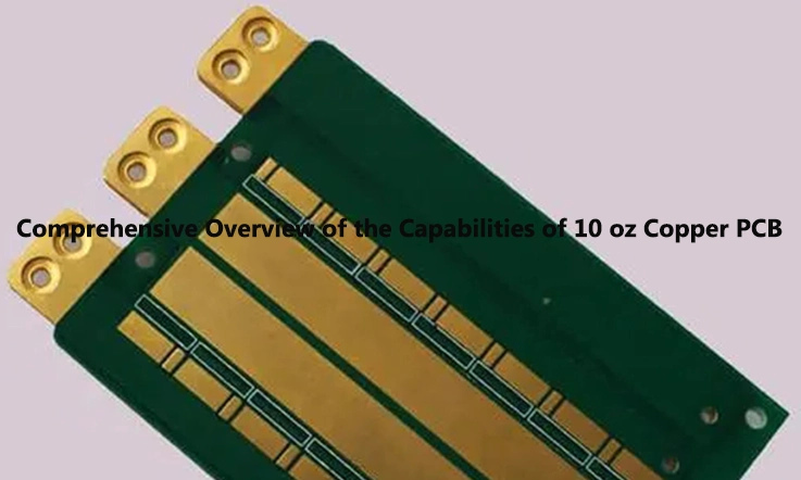
When it comes to high-current and high-power systems, one factor often separates the ordinary from the extraordinary: the PCB material. Not just any material will do when your system needs to carry massive currents, operate in high-power environments, and endure extreme temperatures. For design engineers and manufacturers, 10 Oz Copper PCBs have emerged as a solution that meets these demands with unparalleled efficiency.
What makes 10 Oz Copper PCBs stand out is their ability to handle greater electrical loads, offer enhanced thermal management, and maintain durability over extended periods of use. These capabilities make them good for industries like electric vehicles, aerospace, industrial power systems, and even military applications. This guide will take you through the design considerations, manufacturing techniques, and real-world applications of 10 Oz Copper PCBs, helping our engineers understand how to make the most of these robust circuit boards.
The Rising Demand for 10 Oz Copper PCBs in High-Performance Systems
The demand for 10 Oz Copper PCBs is rising rapidly as industries push the envelope in high-power electronics. As power systems become more sophisticated and require higher efficiency, the need for thicker copper layers has never been clearer. 10 Oz Copper PCBs stand out due to their superior current-handling capacity, excellent thermal dissipation properties, and overall reliability in demanding applications.
From industries like electric vehicles (EVs), where battery management systems demand high levels of electrical throughput, to solar energy systems that rely on efficient energy conversion and long-term durability, 10 Oz Copper is becoming the go-to solution for high-performance applications. Let’s dive into how these factors shape the way industries adopt this advanced technology.
The Evolution of Power Electronics
Power electronics have come a long way from their early days, when the use of thin copper layers was sufficient for low-current applications. As power requirements grew with the development of modern electronics, traditional designs could no longer cope with the increasing demands for higher current capacity and better thermal management.
Enter the 10 Oz Copper PCB. A thick copper layer, up to 10 ounces per square foot, can handle far more current without significant resistance buildup, making it perfect for high-power systems. With increased demand for energy-efficient solutions and sustainable power systems, industries needed a more robust solution that could provide both high current-handling and heat dissipation.
This evolution has led to 10 Oz Copper PCBs becoming the new industry standard for any high-current application. These boards offer the necessary support to next-gen power systems, including electric vehicle charging stations, renewable energy grids, and even aerospace technologies. Simply put, if you’re pushing a high-current system to its limits, you’ll want a board that can handle the pressure — and that’s exactly what 10 Oz Copper delivers.
Understanding High-Current PCB Challenges
In the world of high-current PCB design, heat and resistance are the two biggest headaches that we face. The higher the current, the more heat gets generated in the system, leading to potential thermal damage, degradation of performance, and even component failure. 10 Oz Copper PCBs provide an effective way to tackle these challenges.
One of the primary concerns for us is trace resistance. As current flows through a copper trace, it experiences resistance, which results in heat generation. The thicker the copper, the lower the resistance, and the better the thermal conductivity. This is where 10 Oz Copper shines. It allows for larger trace widths, reducing the overall resistance and allowing the system to carry more current with less heat buildup.
Another significant challenge is thermal stress. Overheating can lead to PCB failure if the design doesn’t account for heat dissipation. Fortunately, 10 Oz Copper provides a solution by not only conducting electricity effectively but also helping to spread heat more evenly across the board. This reduces the risk of localized overheating and ensures long-term reliability.
For our designers, this means we can push systems to higher current loads without worrying about resistance-related issues or thermal failures. Simply put, 10 Oz Copper PCBs make handling high-power applications more manageable, keeping systems safe and operational under heavy loads.
Why Industries Need the 10 Oz Copper Advantage?
It’s clear that 10 Oz Copper PCBs offer several advantages over traditional copper boards, especially for high-current applications. But what exactly makes these PCBs indispensable for modern industries?
Industries such as renewable energy, automotive, aerospace, and even military systems are demanding more from their electronic systems — higher current-carrying capacity, better thermal management, and improved system longevity. For example, in electric vehicle charging stations, the PCB is responsible for power conversion and battery management. With 10 Oz Copper, the PCB can support higher current without suffering from heat-related issues, making these systems more efficient and long-lasting.
In solar power systems, 10 Oz Copper PCBs handle high-current flow from solar panels to inverters. The thick copper layers ensure that the solar power systems can operate at peak efficiency without overheating, even under high load conditions. For military electronics like radar systems, where high currents and thermal dissipation are a must, 10 Oz Copper PCBs ensure that these systems work reliably under extreme conditions, from high temperatures to physical stress.
By utilizing 10 Oz Copper, industries can build robust, reliable systems that are designed to withstand the rigors of modern high-current, high-power applications. It’s no longer just a question of meeting demand — it’s about exceeding expectations.
What is a 10 Oz Copper PCB?
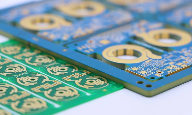
About high-performance electronics, 10 Oz Copper PCBs have found their place as a reliable solution for managing higher currents and ensuring better heat dissipation. These PCBs are specifically designed for demanding applications, from electric vehicles to renewable energy systems. But how does the 10 Oz Copper differ from other types, and why is it a preferred choice for such applications? Let’s take a deeper look.
In this section, we’ll break down the core details of 10 Oz Copper PCBs and explain how the thickness of the copper layer plays a role in supporting high-current circuits. We’ll also touch on how these boards support the thermal management and reliability needed in high-demand environments.
Definition and Purpose of 10 Oz Copper in PCB Manufacturing
What is 10 Oz Copper? In the PCB world, the term 10 Oz Copper refers to a measurement of the copper’s thickness—approximately 350 microns per square foot. This increased thickness provides the necessary material to handle higher current loads, especially in systems where significant power flow is required.
A 10 Oz Copper PCB is built to manage the electrical current and heat generated in high-power applications like electric vehicles, solar energy systems, and industrial equipment. Unlike regular copper boards, which are typically thinner, 10 Oz Copper PCBs offer the performance needed to handle more demanding electrical environments.
Thick copper PCBs are commonly used when higher current handling and heat dissipation are needed to ensure the stability of the system. In high-power electronics, using copper with increased thickness helps prevent overheating and system failure due to inefficient thermal management.
Call to Action: For industries that rely on powerful electronic systems, transitioning to 10 Oz Copper PCBs might just be the answer to boosting performance and durability. These boards are a solid solution for heavy-duty applications that require long-term reliability.
Comparing 10 Oz Copper with Standard PCB Copper Thickness
Now, let’s dive into the comparison between 10 Oz Copper PCBs and those that use standard copper thickness. This comparison highlights the reasons why 10 Oz Copper is often the preferred choice for high-current systems.
Typically, standard PCB copper thickness ranges from 1 oz to 3 oz per square foot. While these boards are suitable for consumer electronics and some mid-power systems, they don’t meet the demands of high-power applications where greater current and heat management are necessary. Let’s see how 10 Oz Copper PCBs fare in comparison:
1.Current Handling Capacity: With 1 oz copper, the traces are limited in terms of how much current they can handle. As the current increases, the traces can begin to overheat or fail. However, 10 Oz Copper PCBs are designed to carry a much larger amount of current without compromising performance.
2.Thermal Management: The thicker copper layers in 10 Oz Copper PCBs are more effective at distributing heat across the board. In comparison, standard copper boards are more prone to localized hotspots under heavy loads, which can negatively impact the overall performance and lifespan of the system.
3.Trace Resistance: Resistance is lower in thicker copper traces, which helps reduce energy loss and keeps the circuit efficient. As the copper thickness increases, the trace resistance decreases, making 10 Oz Copper a better option for ensuring efficient current flow in high-power systems.
Example: A solar power converter with standard copper PCB might face issues with overheating and efficiency loss after extended use. On the other hand, 10 Oz Copper PCB technology allows the converter to handle greater electrical loads while maintaining optimal heat distribution—ultimately extending the system’s lifespan and reducing the risk of failure.
Comparison of Copper Thickness and Performance in High-Power Systems-
| Copper Thickness | Current Handling Capacity | Thermal Dissipation | Applications |
| 1 oz per sq ft | Low | Moderate | Consumer Electronics |
| 3 oz per sq ft | Moderate | Better | Automotive, Mid-Power Systems |
| 10 oz per sq ft | High | Excellent | Electric Vehicles, Solar Inverters, Military Electronics |
Call to Action: For projects that demand high-performance standards, 10 Oz Copper PCBs deliver reliability and durability in the long run. Whether you’re working on renewable energy solutions or high-power industrial systems, these boards are engineered to meet the toughest challenges.
Key Benefits of 10 Oz Copper PCBs for High-Power Applications
As demand grows for high-power electronics, the need for effective PCB materials increases. 10 Oz Copper PCBs are gaining traction for applications that require high current-carrying capacity, effective thermal dissipation, and long-lasting performance. These heavy copper PCBs are frequently chosen in industries like automotive, renewable energy, and industrial controls. Their ability to handle high electrical loads, manage heat efficiently, and maintain durability in tough conditions makes them suitable for systems that require continuous operation without failure.
Enhanced Electrical Conductivity and Current-Carrying Capacity
The 10 Oz Copper PCB is made with a thick copper layer, enhancing its ability to carry high currents without excessive resistance. This thicker copper allows the PCB to manage large electrical loads effectively, ensuring reliable performance in high-power systems.
Using 10 Oz Copper (10 ounces of copper per square foot), these PCBs ensure minimal electrical resistance and voltage drop even in demanding situations. The thicker copper layer permits the inclusion of larger traces that lower resistance, ensuring the board can handle substantial electrical current without compromising on efficiency. Compared to traditional copper PCBs, which have thinner layers (1 oz, 2 oz, or 3 oz per square foot), 10 Oz Copper PCBs provide a more effective solution for managing high-current systems.
| Copper Thickness | Current-Carrying Capacity | Resistivity | Common Applications |
| 1 oz per sq ft | Low | Higher | Consumer electronics, low-power systems |
| 3 oz per sq ft | Moderate | Moderate | Automotive, mid-power systems |
| 10 oz per sq ft | High | Low | Power inverters, EV chargers, industrial systems |
The lower resistivity of the 10 Oz Copper PCB reduces the heat generated during power transmission, allowing for safer operation in high-power applications.
Superior Thermal Management and Heat Dissipation in 10 Oz Copper PCBs
Thermal management is an essential aspect of high-power PCBs. 10 Oz Copper PCBs enhance heat dissipation thanks to the thick copper layer, which ensures better heat conductivity. In applications where heat buildup can lead to system malfunction or failure, the thick copper layer aids in transferring the heat more effectively, allowing for smoother operation of the system.
A thicker copper layer helps spread the heat more evenly across the PCB, reducing the formation of hotspots. Thermal vias incorporated into these designs create effective paths for heat to transfer from the copper to the surface of the PCB, facilitating heat release into the surrounding environment. The addition of thermal vias and heat sinks can further assist in managing heat and reducing the risk of overheating in high-power systems.
| Copper Thickness | Thermal Conductivity | Heat Dissipation Efficiency | Thermal Management Techniques |
| 1 oz per sq ft | Low | Low | Basic vias and heat sinks |
| 3 oz per sq ft | Moderate | Moderate | Thermal vias and heat sinks |
| 10 oz per sq ft | High | High | Thermal vias, heat sinks, copper filling |
The 10 Oz Copper PCB provides better thermal conductivity than standard copper, ensuring high-power systems like solar inverters and electric vehicle charging stations can operate within safe temperature ranges.
Increased Durability and Reliability in Harsh Environments
The 10 Oz Copper PCB is built to endure mechanical and environmental stress. The added copper thickness enhances structural durability, which is valuable in high-power applications where systems are exposed to physical stress, vibration, or extreme environmental conditions.
The thicker copper layer helps improve the PCB’s mechanical strength. This makes 10 Oz Copper PCBs more resistant to vibration, temperature fluctuations, and thermal expansion, factors that could otherwise damage the PCB over time. These characteristics make 10 Oz Copper PCBs ideal for environments like automotive systems, aerospace, and military electronics, where high levels of stress and temperature changes are common.
| Environment | Challenges | PCB Requirements | 10 Oz Copper PCB Performance |
| Automotive | Vibration, temperature extremes | High durability, mechanical strength | High resilience to mechanical stress |
| Aerospace | Extreme temperatures, vibration | Temperature stability, vibration resistance | Superior heat management and vibration resistance |
| Industrial Control | Harsh chemicals, moisture | Corrosion resistance, high reliability | Corrosion-resistant, long-term durability |
The 10 Oz Copper PCB also performs well in corrosive environments, contributing to long-term reliability and ensuring that high-power systems continue to operate without issues despite harsh conditions.
Designing and Fabricating 10 Oz Copper PCBs for Complex Systems
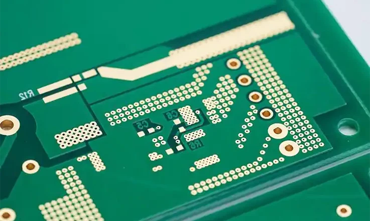
As demand for high-power systems grows, 10 Oz Copper PCBs are increasingly used in applications that require handling heavy electrical loads and managing thermal output. These boards are designed to support larger currents while maintaining stability and managing heat. The design and production of 10 Oz Copper PCBs involve selecting appropriate materials, creating multi-layer stack-ups, and incorporating advanced thermal management techniques. These considerations ensure reliable operation in systems like automotive controllers, industrial robots, and power converters, even in challenging environments.
The design process for 10 Oz Copper PCBs involves selecting materials that offer current handling capabilities, creating PCB stack-ups that optimize both electrical performance and heat dissipation, and using thermal management techniques that prevent overheating. Let’s explore the specifics of these design elements.
Material Selection: Copper Foil and Base Materials for 10 Oz Copper PCBs
When designing 10 Oz Copper PCBs, the choice of copper foil and base materials is fundamental to ensuring both electrical performance and durability. The copper foil used for 10 Oz Copper PCBs is significantly thicker than the standard copper foils found in typical PCBs. The extra thickness provides the necessary current-handling capabilities for high-power applications, where currents may exceed typical ranges.
The base materials selected for the PCB also contribute to its overall performance. Materials like FR4 and ceramic-based substrates are commonly used, providing the mechanical strength required to handle high thermal and electrical stress. Polyimide and Teflon-based substrates may also be used when additional thermal stability is needed, particularly in industries like automotive and aerospace where extreme conditions are often encountered.
| Material | Purpose | Characteristics | Applications |
| Copper foil (10 oz) | High current handling | High conductivity, low resistivity | Electric vehicle charging systems, power inverters |
| FR4 | Structural support and insulation | Excellent dielectric properties | General use in industrial control systems |
| Polyimide | Thermal stability and flexibility | High temperature resistance | Aerospace, automotive electronics |
| Teflon | Superior electrical performance | Low dissipation factor, high insulation | High-frequency, high-power applications |
These materials ensure that 10 Oz Copper PCBs can manage electrical loads and thermal fluctuations effectively, contributing to the overall reliability of the system.
Stack-Up Design: Multi-Layer Solutions for 10 Oz Copper PCBs
For high-power applications, the stack-up design of 10 Oz Copper PCBs is fundamental to meeting both current-carrying and thermal dissipation requirements. The stack-up design refers to how the layers are arranged and the number of layers used to support the necessary current handling and signal integrity.
In 10 Oz Copper PCBs, thicker copper layers are used on the outer layers to handle the increased electrical current. Inner layers can be used for signal routing and power distribution. These multi-layer PCB stack-ups are designed to ensure that the traces can handle high currents without excessive resistance, which could lead to overheating.
| Layer Type | Purpose | Copper Thickness | Applications |
| Outer Layers | High current capacity, heat dissipation | 10 oz | Power distribution, automotive control systems |
| Inner Layers | Signal routing, power distribution | 1 oz – 3 oz | Complex systems like industrial robots and electric vehicles |
| Core Material | Structural support, insulation | Varies | General use in high-power applications |
The multi-layer stack-up ensures the board maintains electrical and thermal stability, making it suitable for industrial robots and power supplies, where reliable current handling and heat management are essential.
Advanced Thermal Management for Heavy Copper PCBs
In high-power applications, managing heat effectively is a must to prevent overheating and maintain system stability. The thicker copper layers in 10 Oz Copper PCBs are designed to spread heat more evenly, helping to minimize the chances of thermal damage. To enhance heat transfer, thermal vias are commonly employed in these PCBs, creating a direct path to move heat from the inner layers to the outer surface or heat sink. This design approach ensures that heat doesn’t become a limiting factor in performance, keeping the system running smoothly under load.
Thermal vias improve heat transfer efficiency, helping to spread heat evenly across the PCB, preventing localized hotspots that could lead to failure. In some designs, heat sinks or thermal pads are used to further aid in heat dissipation, transferring heat from the PCB to surrounding components or the external environment.
| Thermal Management Feature | Function | Benefit | Applications |
| Thermal vias | Direct heat transfer from inner layers | Prevents overheating and ensures uniform heat distribution | Electric vehicle charging stations, industrial equipment |
| Heat sinks | Enhanced heat dissipation | Improves heat removal from the PCB | Power supply systems, solar energy inverters |
| Thermal pads | Thermal interface between PCB and external cooling systems | Optimizes heat transfer to external devices | Military electronics, automotive power systems |
Using advanced thermal management techniques, 10 Oz Copper PCBs can operate effectively in demanding environments, ensuring long-term reliability in high-power applications.
Manufacturing Challenges and Solutions in 10 Oz Copper PCB Production
10 Oz Copper PCB production presents a set of unique challenges due to the increased copper thickness and the power demands of these boards. These challenges require precision and advanced techniques to ensure the PCBs meet the requirements of high-current applications. In this section, we will delve into the common difficulties encountered during heavy copper PCB fabrication and how we address them to maintain the necessary performance and durability.
From precision etching to copper plating, the production of 10 Oz Copper PCBs requires specialized processes to ensure the copper thickness, uniformity, and overall quality are adequate for the intended applications. Furthermore, As PCB manufacturers, we must adhere to rigorous quality control standards to ensure the PCBs perform as expected in demanding environments like automotive electronics, industrial systems, and energy conversion applications.
Precision Etching for Heavy Copper Layers
Etching is a core process in PCB fabrication, especially when dealing with the heavy copper layers required in 10 Oz Copper PCBs. The increased copper thickness makes it more challenging to achieve precise etching without compromising the material’s integrity. Standard etching techniques are often insufficient for heavy copper PCBs, leading to uneven traces and potential loss of conductivity or thermal efficiency.
To overcome this challenge, advanced etching techniques such as laser etching, plasma etching, and chemical etching are employed. These methods ensure the copper layers are etched accurately, allowing for clean, well-defined traces and pads without compromising the copper’s conductivity.
Laser etching, in particular, has gained popularity due to its ability to precisely remove copper from specific areas, ensuring fine details and consistent results. This method is well-suited for power distribution systems, battery management circuits, and electric vehicle charging stations, where precise design is essential.
| Etching Technique | Description | Advantages | Applications |
| Laser etching | Uses laser beams to etch copper with high precision | High accuracy, minimal material wastage | Automotive control systems, power circuits |
| Plasma etching | Uses ionized gas to etch copper | Quick processing, uniform etching | Renewable energy systems, heavy power applications |
| Chemical etching | Uses acid or other chemicals to remove copper | Cost-effective for large-scale production | General PCB manufacturing, industrial systems |
By utilizing these advanced etching methods, we can achieve the desired copper trace patterns while maintaining the required electrical and thermal performance of the 10 Oz Copper PCBs.
Plating and Laminating Techniques for Heavy Copper PCBs
In 10 Oz Copper PCB production, copper plating and lamination are another steps to ensure uniformity and durability. These processes ensure the PCB’s copper layers bond correctly to the substrate and maintain the necessary performance for high-current applications.
Copper plating involves the deposition of a thin layer of copper onto the PCB substrate. This process must be closely controlled to ensure that the copper is evenly deposited, particularly in heavy copper PCBs, where achieving uniform plating is more challenging due to the thicker copper layers.
Lamination, which bonds the copper foil to the PCB substrate, requires careful control of temperature and pressure to avoid defects such as air bubbles or uneven adhesion. Any imperfections during this process can lead to issues in electrical and thermal performance.
To ensure that the 10 Oz Copper PCBs meet the demands of high-current applications, electroplating is often used for better adhesion, while controlled lamination is essential to avoid thermal expansion problems.
| Technique | Purpose | Challenges | Applications |
| Copper plating | Ensures copper deposition on PCB layers | Maintaining uniform thickness and adhesion | High-power electronics, battery management |
| Lamination | Bonds copper foil to PCB substrate | Avoiding imperfections in adhesion and thickness | Heavy-duty industrial equipment, renewable energy |
| Electroplating | Ensures better adhesion between copper layers | Controlling thickness uniformity | Automotive power systems, power converters |
Through effective plating and lamination techniques,so we can ensure that 10 Oz Copper PCBs are both durable and capable of handling high currents for a range of demanding applications.
Quality Control Standards and Testing in 10 Oz Copper PCB Production
Ensuring consistent quality throughout the production of 10 Oz Copper PCBs is non-negotiable, especially when these boards are used in sectors where dependability is a must. To meet the performance standards required by these applications, we stick to rigorous quality control measures. From the selection of materials to the final inspection, every step is managed carefully to guarantee that the finished product can handle the tough conditions it’ll face in real-world scenarios. Our approach keeps the production line steady, ensuring each PCB meets the required specs without fail.
The IPC-2221 standard provides design and manufacturing guidelines to ensure that 10 Oz Copper PCBs are fabricated to meet industry expectations. Likewise, IPC-A-600 outlines visual acceptability criteria to ensure no visible defects are present in the final product.
In addition to these standards, comprehensive testing procedures such as electrical testing, thermal testing, and visual inspections are used to verify the PCB’s functionality under real-world conditions. These tests check for the PCB’s ability to handle the required electrical loads and heat dissipation, ensuring long-term reliability.
| Test Type | Purpose | Method | Application |
| Electrical testing | Verifies electrical conductivity and current handling | Automated testing, continuity checks | Power distribution systems, industrial control |
| Thermal testing | Ensures heat dissipation and stability | Thermal cycling, heat mapping | Electric vehicle charging systems, energy conversion |
| Visual inspections | Checks for defects in the copper layers and overall PCB | Manual inspection, automated optical inspection | Aerospace electronics, high-power circuits |
Managing Quality Control in 10 Oz Copper PCB Production
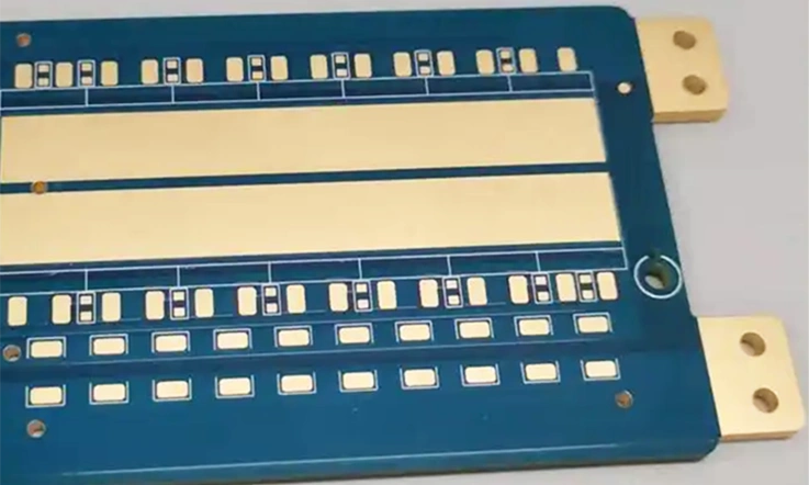
Achieving high quality in the production of 10 Oz Copper PCBs involves rigorous checks and continuous oversight at each stage of the manufacturing process. The methods used to ensure consistent performance of these heavy copper PCBs can vary depending on the design, materials, and production techniques. Below is an outline of effective quality control measures implemented throughout the production lifecycle.
Design Validation and Pre-Production Checks
Before production begins, it’s necessary to thoroughly review the PCB design and check it for any potential issues. The process starts with conducting detailed design rule checks (DRC) and manufacturing rule checks (MRC) to ensure everything is in line with the required standards. These checks help identify design flaws early on, preventing issues that could affect the electrical, mechanical, or thermal performance of the PCB later in the process. By focusing on this step, we can avoid setbacks in the later stages and ensure the design is robust and prepared for production.
The goal here is to ensure that trace widths are sufficient for high current flow, and that via sizes and placements are optimized to avoid unnecessary heat accumulation. During design validation, we can simulate the actual operating conditions of the PCB to confirm that it meets performance requirements under high-load conditions.
Key steps include:
●Running DRCs to identify design flaws.
●Performing MRCs to ensure manufacturability.
●Validating thermal and electrical simulations.
Material Selection and Quality Assurance
The quality of materials used in 10 Oz Copper PCBs directly influences the final product’s performance. The copper foil chosen must meet precise thickness specifications, ensuring that it can handle the required current without excessive resistance. Likewise, dielectric materials and laminates need to be selected based on their ability to endure high temperatures and prevent breakdown under stress.
Using materials that meet industry standards, such as copper foil with a thickness tolerance of ±5%, ensures that the PCB maintains high electrical conductivity and thermal stability. Non-compliance with material specifications during production can result in poor performance and early failure in high-current applications.
Material Selection Considerations:
| Material Type | Specification | Purpose |
| Copper Foil | 10 Oz (350 µm) ±5% | High-current carrying capacity |
| Dielectric Layer | FR4 or high-temperature resin | Insulation and thermal stability |
| Laminate | Standard or custom laminate | Base structure for copper foil |
Process Control During Fabrication
Process control involves maintaining precise conditions throughout the manufacturing process. Stages like lamination, etching, drilling, and plating require constant monitoring to ensure consistency and accuracy. For example, during lamination, controlling the temperature and pressure is necessary for proper copper bonding to the base material. Any variation in these conditions can result in weak spots or incomplete adhesion. By carefully managing these steps, we can ensure that the final product meets the required standards without unexpected issues.
Process Control Measures:
●Lamination: Monitor pressure and temperature profiles to ensure consistent copper bonding.
●Etching: Adjust etching parameters to ensure precise trace patterns without under-etching or over-etching.
●Drilling and Plating: Ensure that drilling operations maintain proper hole sizes and plating thicknesses.
Testing and Inspection Throughout Production
Comprehensive testing and inspections are conducted at multiple stages during production to ensure the integrity and functionality of 10 Oz Copper PCBs. Electrical tests, such as continuity testing and high-voltage testing, are employed to verify the PCB’s ability to handle current and operate within the required voltage range. In addition to electrical testing, physical inspections are performed to detect any visual defects such as misaligned traces or solder mask issues.
Testing Methods:
| Test Type | Purpose | Measurement |
| Continuity Testing | Check for circuit integrity | Ensures no open circuits or shorts |
| High Voltage Testing | Simulate high-power conditions | Verifies the PCB can withstand higher voltages without breakdown |
| Insulation Resistance | Confirm dielectric integrity | Ensures proper insulation between traces |
Quality Assurance and Documentation
Keeping detailed records of materials, processes, and tests helps ensure everything aligns with quality standards. . This documentation serves not only as proof of quality but also as a reference for troubleshooting in case of future issues. These records include:
●Material certification reports.
●Process control logs.
●Test reports from electrical and physical inspections.
●Any non-conformance reports outlining issues found during inspections.
This documentation allows us to trace every aspect of production and ensures that all standards and regulations are adhered to. The continuous review and improvement of quality standards help to maintain a consistent production process, even as new designs or materials are introduced.
Design Challenges and Solutions for 10 Oz Copper PCBs
When designing 10 Oz Copper PCBs, we face multiple challenges, particularly around handling high-current applications and ensuring effective heat management. These boards are commonly used in systems like automotive power control, industrial automation, and high-power electronics, where the PCB’s reliability and efficiency can directly impact system performance.
As the need for heavy copper PCBs increases, we must address factors like optimizing current flow, managing heat dissipation, and minimizing potential risks in high-power environments. In the following sections, we’ll explore common design challenges and methods to overcome them, ensuring that 10 Oz Copper PCBs continue to meet the demands of advanced applications.
Optimizing High-Current Flow in Complex PCB Designs
High-current applications in 10 Oz Copper PCBs require careful attention to current flow to avoid excessive resistance, which can lead to thermal buildup and system inefficiency. To handle these high-power demands, the trace width of the PCB needs to be carefully designed. With the increased copper thickness of 10 Oz Copper, the trace must be wide enough to carry higher currents without causing significant temperature rise. Adjusting the trace width properly allows for effective heat dissipation and keeps the system performing as expected.
we often use trace width calculators to determine the appropriate trace dimensions that will provide the best current-carrying capacity, while keeping resistance in check. This step helps ensure that the copper traces effectively distribute the electrical load, minimizing the risk of overheating. Another consideration is optimizing current paths, which can be done by designing PCB layouts that balance the electrical load across the board’s layers.
In addition, we also use layer stacking in multilayer PCB designs to evenly distribute the current and reduce the chances of localized heating. Using wider traces, adjusting layer configurations, and implementing thermal vias are all strategies that help 10 Oz Copper PCBs maintain efficient current flow.
| Design Method | Purpose | Application |
| Wider traces | Reduces resistance, improves current capacity | Automotive power systems, renewable energy converters |
| Layer stacking | Distributes current across multiple PCB layers | High-power electric systems, power electronics |
| Thermal vias | Enhances heat distribution by connecting copper layers | Industrial control boards, electric vehicle charging units |
Addressing Thermal Challenges in High-Power PCB Systems
Thermal management is a major challenge in high-power PCB systems like those incorporating 10 Oz Copper. As current flows through the copper traces, it generates heat. Without effective management, this heat can degrade the performance of the PCB and compromise its lifespan.
To manage heat, we can use thermal vias and heat sinks to facilitate heat transfer away from the critical areas of the PCB. Thermal vias are particularly useful in heavy copper PCBs, as they connect different layers and allow heat to flow more efficiently from one layer to another, minimizing temperature fluctuations. Heat sinks are often added to areas with the highest thermal loads, ensuring effective cooling.
Another technique to address thermal concerns is adjusting copper thickness. The thicker the copper, the more heat it can absorb and distribute. In 10 Oz Copper PCBs, the increased copper thickness helps to dissipate heat more effectively, making these boards more resilient in high-power applications.
| Thermal Management Technique | Function | Benefit |
| Thermal vias | Transfers heat between layers to distribute thermal energy | Prevents overheating, ensures steady operation |
| Heat sinks | Absorbs and disperses heat from high-thermal zones | Aids in keeping temperature levels manageable |
| Copper thickness | Allows copper to absorb and spread heat more effectively | Reduces the risk of localized heat damage |
Using these methods, 10 Oz Copper PCBs can operate effectively within the temperature constraints of high-current systems, ensuring they remain reliable over time.
Mitigating Design Risks and Enhancing Reliability
In high-power systems, the challenge extends beyond just handling current and heat—it’s also about ensuring that the PCB remains reliable over time. Factors like signal integrity, environmental stress, and copper migration can influence PCB performance, so these risks must be addressed during the design phase.
To ensure clear signal transmission, we use controlled impedance designs, which help maintain the integrity of signals as they move through the PCB. In high-power applications, maintaining low impedance in the traces is essential, as higher impedance could mess with the signal and cause loss or distortion. By carefully adjusting the impedance to match the requirements, we can make sure the signals stay sharp and strong, even when the current levels are cranked up.
Additionally, copper migration can occur when the high currents cause gradual erosion of the copper traces, so it is necessary to ensure proper trace width and copper plating. Protective measures like conformal coatings can also be applied to reduce the risk of copper oxidation and environmental damage.
By running electrical tests and environmental stress tests, we ensure that the 10 Oz Copper PCBs are up for the challenge in real-world environments. This testing process is a must, especially in applications like industrial robotics or power supplies, where any failure simply isn’t an option. These tests simulate harsh conditions and extreme usage to give us confidence that the PCBs will perform reliably when the pressure’s on.
| Design Risk Mitigation Method | Purpose | Benefit |
| Controlled impedance design | Ensures signal stability across the PCB | Prevents signal loss or distortion in high-power systems |
| Conformal coatings | Protects the PCB from environmental factors like moisture | Reduces risk of copper migration and enhances reliability |
| Environmental stress testing | Verifies the PCB’s durability under real-world conditions | Ensures long-term reliability in extreme environments |
Why Choose Us?
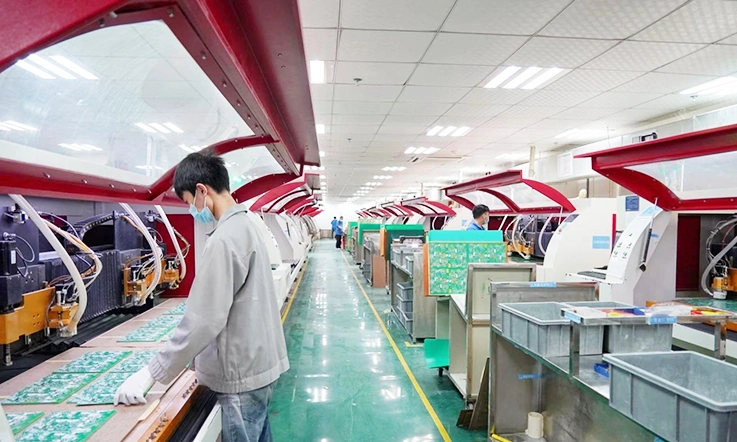
Your Trusted 10 Oz Copper PCB Manufacturer and Supplier in China
At JarnisTech, we are committed to delivering high-quality 10 Oz copper PCBs for a wide range of demanding applications. As a leading manufacturer and supplier based in China, we take pride in our craftsmanship and dedication to meeting our clients’ specific needs. Our years of experience and technical expertise ensure that your project is handled with precision and care from start to finish.
Why Our clients Choose Us?
1.Adherence to Industry Standards: All of our printed circuit boards meet IPC Class 2 or Class 3 standards, ensuring reliable performance and durability in various applications. We strive for consistency and quality, providing products that meet your exact specifications, whether for consumer electronics, industrial machines, or automotive systems.
2.Decades of Expertise: With over two decades of experience in the field of PCB manufacturing, especially for heavy copper 10 Oz PCBs, we’ve honed our skills and deepened our knowledge of advanced PCB fabrication processes. Our team’s extensive experience guarantees that every board is produced with the highest level of precision.
3.Thorough CAM Review Before Manufacturing: To ensure that your files are free from errors and that the production process is optimized for efficiency, all files undergo a thorough CAM (Computer-Aided Manufacturing) review. This step helps catch any potential issues early, saving time and ensuring high-quality outcomes.
4.Flexible Order Quantities: Whether you’re placing a small batch order for a prototype or need a larger production run, we don’t require a minimum order quantity for new orders. This flexibility allows you to get the exact quantity you need for your project, whether it’s a one-off design or large-scale production.
5.Dedicated Support Team: Our professional sales and engineering support teams are available full-time to assist with any questions or concerns you may have. We’re here to ensure your project is completed on time and within budget, offering tailored advice and solutions along the way.
Our Heavy Copper/Thick Copper PCB Manufacturing Capabilities:
| Manufacturing Capability | Details/Specifications |
| Copper Thickness | >10 Oz Copper (350 µm per layer) |
| PCB Type | Heavy Copper PCB/Thick Copper PCB |
| Board Thickness | Up to 8.2 mm |
| Trace Width | Minimum 0.2 mm (8 mils) |
| Via Types | Through-hole, Blind, Buried, Thermal vias |
| Thermal Management | Thermal vias, copper planes, heat sinks |
| Lamination | High-performance dielectric material for heavy copper layers |
| Plating | Electroplating for copper layers |
| Surface Finish | HASL, ENIG, OSP |
| Testing | Continuity, insulation resistance, high-voltage testing |
| Quality Standards | IPC Class 2, IPC Class 3 |
| Prototyping | Quick-turn prototyping, no minimum order quantity required |
| Lead Time | Prototypes: 3-5 days; Production: 7-15 days |
| Assembly | Component mounting, soldering, complete assembly |
We’re Ready to Meet Your Needs
With a solid track record and a commitment to excellence, JarnisTech is your trusted partner for high-performance 10 Oz copper PCBs. Whether you’re looking to discuss the specifics of your project or have any inquiries about our manufacturing process, we invite you to reach out. Let’s talk about how we can support your next project and provide the copper PCB solutions you need.
FAQ & 10 Oz Heavy Copper PCB
1.Can 10 Oz Copper PCBs be used for high-frequency applications?
Typically not ideal for high-frequency applications due to the thicker copper, which may cause signal integrity issues at high frequencies.
2.How do you handle the design of traces in 10 Oz Copper PCBs?
Traces are designed with wider widths to handle the higher current, ensuring minimal resistance and thermal buildup.
3.What is the maximum current capacity a 10 Oz Copper PCB can handle?
The current capacity depends on the board design and trace width but can support up to 100A or more per trace with proper thermal management.
4.How does a thicker copper layer affect PCB rigidity?
The thicker copper layer increases the rigidity of the PCB, making it more durable and suitable for harsh environments.
5.Can 10 Oz Copper PCBs be used for flexible applications?
Due to the thickness of the copper, they are generally rigid, not suitable for flexible PCB designs.
6.Are 10 Oz Copper PCBs more expensive than standard PCBs?
Yes, the manufacturing cost is higher due to the additional copper material and specialized production processes.

