Both single-layer and multi layer PCB are frequently exploited in a broad spectrum of applications. Single-layer PCB typically find their place in less sophisticated devices that demand only rudimentary functions, whereas multilayer PCB are adeptly matched for more intricate devices that call for heightened functionality. The demand for multi-layer circuit board has been on the rise in recent times, driven by the requirement for smaller and more intricate devices across various industries and sectors.
Multilayer PCBs are extensively employed in professional electronics including computing devices, cellular handsets, and cardiac monitors, to mention just a few. The production process of these multilayer PCBs entails laminating in excess of two conductive layers together, with the layer count being contingent upon the specific requirements of the application. The provision of multiple layers within the PCB permits the consolidation of extra circuitry and wiring, hence facilitating the execution of more sophisticated functionality. For instance, mobile phone PCBs can incorporate as many as 12 layers to accommodate the intricate nature of these devices.
Definition of Multilayer PCB Circuit Board
A multi layer PCB refers to a type of circuit board that consists of multiple layers of conductive traces and insulating material laminated together. Contrary to a single-layer or double-layer PCB, these simple circuit board sport conductive routes exclusively on one side or on both sides of the substrate respectively. However, multilayer Printed circuit board features conductive pathways spanning across multiple strata.
The multilayer PCB’s fabrication process typically comprises the stratification of multiple layers of conductive copper tracks, also acknowledged as signal layers, interspersed with layers of dielectric material, typically designated as prepreg or core layers. The number of layers can vary depending on the complexity and requirements of the circuit design. Regularly adopted multilayer PCB design encompass 4-layer, 6-layer, 8-layer stack up, and configurations extending even beyond these layer counts.
The conductive pathways traversing each layer of a PCB are interconnected via plated apertures, typically referred to as vias. These vias establish the electrical liaison between diverse layers, enabling signal transition through the board along a vertical path. These vias can embody through-hole vias, which permeate through the entire stack of PCB layers, or they could be blind and buried vias, exclusively linking designated layers.
Multilayer PCBs furnish several merits over their single-layer or double-layer counterparts. They allow for increased component density, as more layers provide additional space for routing traces and placing components. Moreover, multilayer PCBs uphold superior signal integrity, minimize electromagnetic interference (EMI), promote effective thermal management, and amplify power distribution proficiencies.
The processes of designing and fabricating multi layer PCB can carry a greater complexity when compared to single or double-layer PCB, owing to the necessity for exact layer alignment, controlled impedance, and thoughtful handling of signal and power integrity. Yet, the merits of multilayer PCB make them fit for an extensive array of applications, such as high-speed digital circuits, intricate electronic systems, and devices with stringent size and performance specifications.
Factors Influencing the Decision to Use Multilayer PCB
Circuit complexity: Multi layer PCB are preferred when the circuit design involves a high number of components, complex interconnections, and a large number of signal traces. The additional layers contribute added routing area, promoting efficient signal transition, minimising intricacy, and improving overall performance.
Component density: If the circuit requires a high component density, where numerous components need to be placed in a limited space, a multi-layer PCB is often chosen. The multiple layers allow for more efficient use of space and enable compact designs.
Signal integrity: Multi-layer PCB are beneficial for circuits that involve high-speed digital signals or sensitive analog signals. The additional layers help control impedance, minimize noise, and reduce signal crosstalk. This ensures better signal integrity and reduces the risk of signal degradation.
Power distribution: In circuits that require multiple power supply voltages or have high power requirements, multi-layer PCB are used to provide dedicated power planes. These power planes facilitate efficient power distribution, reducing voltage drops and minimizing interference between different signal traces.
Thermal management: If the circuit generates significant heat or requires efficient heat dissipation, a multi-layer PCB can incorporate thermal vias and copper planes. These features help spread heat and enhance thermal management, preventing overheating and ensuring reliable operation.
Size constraints: Multi-layer PCB are advantageous when there are size constraints for the electronic device. Leveraging the utility of multiple strata can lessen the total footprint of the PCB, smaller smaller, more compact designs.
EMI/EMC considerations: Electromagnetic Interference (EMI) and Electromagnetic Compatibility (EMC) play a crucial role in electronic design. Multi-layer PCB with proper grounding techniques and shielding layers help minimize EMI emissions and susceptibility, ensuring compliance with regulatory standards.
Cost considerations: multi-layer PCB production incurs a greater expenditure than the manufacturing of single-layer or dual-layer variants. As such, thorough evaluation of the project’s budgetary parameters is essential when determining the feasibility of implementing a multi-layer PCB.
It’s important to analyze these factors and consider the specific requirements of the circuit design, performance goals, size constraints, and budget limitations to determine whether a multi-layer PCB is the most suitable choice for a particular application.
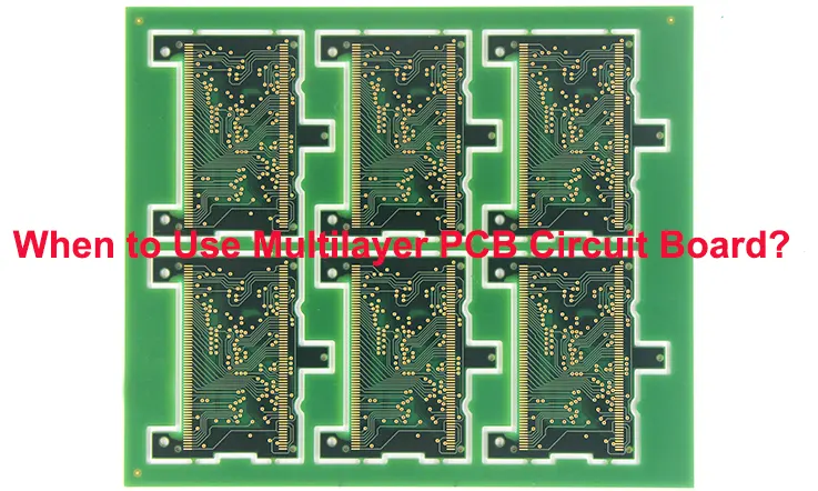
When to Use Multilayer PCB Circuit Board?
Multilayer PCB boards are prevalently utilized in electronic manufacturing, specifically when intricate and compact circuit designs are required. Comprising multiple layers of conductive copper traces divided by insulating layers, these boards facilitate increased functionality and reduced size, in stark contrast to their single or double-layered counterparts.
Multilayer PCBs present significant benefits in a number of situations. Firstly, when a circuit requires a large number of components and interconnections, a multilayer board provides the necessary space for routing traces and accommodating components in a compact manner. This proves especially instrumental in high-density electronic devices such as cell phones, tablets, and computer mainboards.
Multilayer PCBs are also preferred when there is a need for signal integrity and electromagnetic compatibility. The additional layers in these boards provide better control over impedance, minimizing signal loss and crosstalk. This is crucial for high-speed digital circuits, RF applications, and sensitive analog designs.
Furthermore, multilayer PCBs offer enhanced power distribution capabilities. With dedicated power and ground planes, they can efficiently manage power delivery and minimize voltage drops, ensuring stable operation of the circuit and reducing noise interference.
Another advantage of multilayer PCBs is their ability to support complex designs with multiple signal layers. This proves particularly beneficial in circuits necessitating differential signaling, high-sped data transmission, or integrated mixed-signalling.
How to Choose a Reliable Multilayer Circuit Board Partner?
Selecting a dependable multilayer circuit board partner is of paramount importance for any enterprise necessitating top-notch circuit boards. Here are some considerations to ponder over when choice a reliable partner:
1. Experience and expertise: Check their experience in producing similar boards and their ability to meet your specific requirements.
2. Quality assurance: They should follow industry standards and have certifications like ISO 9001 to demonstrate their commitment to quality.
3. Technology and capabilities: To guarantee the production of top notch circuit boards it’s essential for them to have cutting edge pcb manufacturing equipment and keep up and the manufacturing techniques.
4. Design and engineering support: They should have experienced engineers who can provide valuable insights and suggestions.
5. Manufacturing capacity: They should have sufficient capacity to handle your production volume and be flexible enough to accommodate any future growth.
6. Testing and inspection: They should perform rigorous testing to ensure the reliability and functionality of the circuit boards before delivery.
7. Customer support: They should be responsive, offer clear communication channels, and provide timely updates on the progress of your project.
8. Cost-effectiveness: Albeit being a significant factor, cost should not be the singular decisive element. Consider the overall value provided by the partner, including quality, reliability, and technology support, in relation to the cost.
Upon meticulous evaluation of these aspects, you can select a dependable multilayer circuit board associate (Jarnistech), we can will cater to your particular needs and consistently supply top-quality circuit boards.
JarnisTech – Reliable & High-quality Multilayer PCB Manufacturing
JarnisTech Electronic Services stands as your trusted PCB manufacturer. With our broad extensive experience and expertise in the domain, we take pride in our specialization in designing, producing, and providing multilayer PCBs. Irrespective of your necessity for manufacturing or assembly services, our team of PCB connoisseurs stands at your disposal for assistance.
To get started, please feel free to contact us at your convenience. You can get in touch by dialing 0086-755-23034656 or forwarding an email to [email protected]. We understand the significance of your project and are pledged to deliver unparalleled customer service. Our team is enthusiastic about discuss your requirements and provide you with the best solutions tailored to your PCB project needs.
Partner with JarnisTech for reliable multilayer PCB manufacturing and experience the difference of working with a trusted industry leader. We look forward to serving you and exceeding your expectations.
In Conclusion
The advent of multilayer PCB circuit boards has transformed the electronics sector, offering a flexible and proficient resolution for intricate electronic designs. Their capacity to house high-density components, reduce signal disruptions, and boost utility render them a premier choice for a broad assortment of applications.
Be it in consumer electronics, telecommunication industries, medical apparatus, or automotive configurations, multilayer PCB circuit boards persist in marking a pivotal role in technology enhancement. Selecting the a reliable multilayer PCB manufacturer – JarnisTech and mastering the explicit necessities of your project will guarantee that you exploit the utmost capacity of this technology. Harness the benefits of multilayer PCB circuit boards and open up novel opportunities for your electronic designs.
Our services
Multilayer PCB Manufacturing & Assembly

