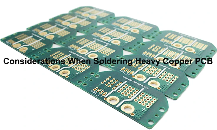
The process of soldering heavy copper PCBs brings unique hurdles influenced by the thicker copper traces and planes, demanding careful consideration to ensure reliable and superior quality solder connections. This manuscript discusses pivotal considerations during the soldering of heavy copper PCBs, including material selection, optimization of soldering operations, control of inspection quality, adhering to best practices in design and layout, and the implementation of in-depth testing and reliability evaluations. Addressing these components can enable manufacturers to achieve successful soldering, thereby enhancing performance and extending the lifecycle of heavy copper PCB assemblies.
What Is Heavy Copper PCB?
A heavy copper PCB designates a printed circuit board characterized by its significantly denser copper traces and planes, setting them apart from standard PCBs. Heavy copper PCBs most often boast a copper denseness of 2 ounces per square foot (oz/ft²) or even denser, which stands in contrast to the standard 1 oz/ft² or less generally observed in conventional PCBs.
Heavy copper PCBs come to the fore in scenarios demanding enhanced current-carrying capacity and superior thermal dissipation. A variety of industries such as power electronics, high-intensity LEDs, automotive electronics, motors and generators, medical equipment, and aerospace and defense systems find noteworthy advantages with these boards.
Incorporation of intense copper traces and planes in heavy copper PCBs opens up a host of beneficial aspects:
Augmented Current Carrying Capacity: Heavy copper, whilst enabling higher currents transmission, also safeguards against risks of excessive voltage drop or overheating. This trait proves explicitly valuable in high-power circumstances.
Superior Thermal Dissipation: The remarkable heat conductivity demonstrated by copper facilitates efficient heat dissipation away from crucial components in heavy copper PCBs, thus circumventing overheating complications.
Diminished EMI/RFI: The pronounced thickness of copper traces and planes serves to minimize electromagnetic interference (EMI) and radio frequency interference (RFI) in heavy copper PCBs.
The fabrication of heavy copper PCBs requires the deployment of specific methodologies and machinery. For instance, electroplating is a frequently used method for layering thick copper traces on the PCB substrate. Consistent control over the electroplating parameters is vital in ensuring homogeneous copper deposition and stable bonding with the substrate.
Heavy copper PCBs, despite their undeniable advantages, carry a few inherent challenges:
Augmented Cost: Due to the complex manufacturing procedures and need for additional materials, heavy copper PCBs generally incur higher costs than standard PCBs.
Increased Weight: The implications of factoring thicker copper traces and planes also include adding heft to the PCB. In applications where weight manipulation is critical, this element must be deliberated upon.
Design Hurdles: Achieving appropriate trace routing and component placement during the PCB design process can become challenging due to the thicker copper traces and planes.
Notwithstanding the hurdles challenges, the relevance of heavy copper PCBs in an extensive spectrum of high-powered and high-performing electronic applications remains paramount. With a comprehensive understanding of design foundations, choice of materials, and production techniques, it becomes feasible to fabricate heavy copper PCBs that efficiently fulfill the requirements of these demanding applications, all while maintaining strict adherence to quality and reliability benchmarks.
Challenges of Soldering Heavy Copper PCBs
Soldering heavy copper PCBs presents unique challenges attributed to their heightened thermal mass and heat dissipation demands. These challenges encompass several critical aspects:
High Thermal Conductivity: Copper, recognized for its exceptional thermal conductivity, promotes efficient heat transfer throughout the PCB. Consequently, obtaining and preserving the necessary temperature at the solder joint could be a challenging process. This difficulty intensifies particularly in areas that accommodate substantial copper pours or thick traces.
Increments in Solder Volume: Establishing reliable solder joints demands more volume of solder for heavy copper PCBs. Yet, in the absence of meticulous control over the soldering process, this can result in problems such as solder bridging, solder balls, and similar defects.
Potential for Warpage and Delamination: The higher temperatures involved in the soldering of heavy copper PCBs can trigger warpage or delamination. This becomes particularly pronounced if the PCB lacks adequate support during the soldering process.
Solder Joint Reliability: The increased thermal and mechanical stresses experienced by heavy copper PCBs elevate the risk of solder joint failures. Consequently, there’s a propensity for reduced reliability and an enhanced risk of component failure.
Machinery Specifications: The soldering of heavy copper PCBs frequently demands the availability of specialized machinery. High-power soldering irons or reflow ovens, which bear the capability for refined control over patterns of heating and cooling, are often requisites in the process.
Resource Planning: The soldering of heavy copper PCBs may be more resource-intensive in terms of cost and time allocation than that of standard PCBs. This is predominantly due to the need for specialized tools and stringent control over the procedures.
These obstacles call for precision and strategic planning. However, with prudent management, heavy copper PCBs continue to represent a notable advancement in the landscape of modern PCB engineering due to the myriad technological benefits they offer.
How Soldering Heavy Copper PCBs?
Soldering heavy copper PCBs necessitates meticulous procedures and specialized methodologies to guarantee optimal outcomes. Here’s an outlined guide on the process:
Equipment Organization: Ensure you have all necessary apparatus within reach. This includes a high-power soldering iron, an apt solder compound, flux, solder paste (if applicable), and any customized tools needed for heavy copper PCBs.
PCB Consideration: Initiate by thoroughly cleaning the PCB to erase any potential contaminants or oxidation from the copper surfaces. This could be achieved using an appropriate PCB cleaning solution or isopropyl alcohol. Ensure your PCB is arid before moving forward.
Component Arrangement: Promptly place your components onto the PCB, taking great care in aligning and arranging them correctly. Keep in mind the increased thermal mass and heat dispersion requirements that characterize heavy copper PCBs during this critical stage.
Flux Dispensing: Distribute a suitable volume of flux to the areas designated for soldering. Flux makes way for a seamless soldering procedure by stimulating optimal wetting and inhibiting oxidation development.
Soldering Protocol: A high-power soldering iron is pivotal to guarantee sufficient heat pass-through when handling heavy copper PCBs. Touch the soldering iron’s end to the joint region to uniformly disperse the heat. Maintain contact until the solder alloy liquefies and forms a polished, mirror-like solder joint.
Solder Dispensation: Introduce the solder compound to the joint area for it to circulate and wet the copper surfaces appropriately. Ensure the solder fully covers the joint without an excess solder volume to prevent solder bridging and related defects. Adopt a soldering iron with strong power capacity to reach and sustain the desired solder joint temperature, counteracting the high thermal conductivity of copper.
Cooling and Review: Let the solder joint cool off naturally. After cooling, conduct a visual examination of the solder joints for any visible defects, such as solder bridges, inadequate solder, or voids. Use a magnifying tool or microscope if necessary for a more detailed observation. Rectify any issues before moving ahead.
Post-Soldering Cleaning: The cleaning process after soldering is crucial for the elimination of any residual flux or solder paste present on the PCB. This can be accomplished by employing an appropriate PCB cleaning agent or isopropyl alcohol. It’s of paramount importance to ascertain that the PCB is thoroughly dry prior to undertaking any additional handling or testing protocols.
Evaluation and Quality Assurance: Undertake comprehensive testing and rigorous quality control checks to ascertain the dependability and functioning of the soldered heavy copper PCB. This could range from electrical tests, functional tests, or inspections utilizing methods like X-ray imaging to discover any hidden anomalies.
Remember that soldering heavy copper PCBs might demand specific process modifications, such as redefining reflow profiles, adjusting temperature patterns, or employing exclusive soldering methods. Adhering to design instructions explicitly tailored for heavy copper PCBs, such as accurate via design, grounding protocols, and thermal management, is highly critical for a successful soldering operation.
To encapsulate, the soldering of heavy copper PCBs warrants a keen eye for detail, the proper toolkit, and obedience to best practices to attain a high-standard and reliable solder joint.
Importance of Proper Consideration
Rigorous contemplation of the challenges and elements tied to soldering heavy copper PCBs is cardinal to attain reliable and superior results. The distinctive attributes of heavy copper PCBs, with their increased thermal mass and heat dissipation demands, call for detailed attention to avert a series of issues such as solder joint inconsistencies (like bridging, balls, and voids), PCB warpage, solder joint reliability reduction, component malfunctions, and heightened production costs and time.
To curb these individual risks and achieve successful soldering of heavy copper PCBs, it is vital to meticulously integrate the ensuing factors:
Materials and Component Selection: Deciding on adequate materials, encompassing copper foil thickness, surface finish, solder alloy, and flux, is a crucial step in effectuating optimal soldering results.
Soldering Process Streamlining: Refining the soldering process via optimizing reflow profiles, temperature changes, and adopting competent soldering methodologies is pivotal to achieve anticipated results.
Inspection and Quality Control Implementation: Instituting rigorous inspection and quality control evaluations, such as visual examination, X-ray investigation, and electrical tests, are invaluable in identifying and correcting any looming defects or issues.
Design and Layout Best Practises: Compliance with industry best practices for design and layout, including via design, grounding techniques, and robust thermal management strategies, significantly aid in the successful soldering of heavy copper PCBs.
Total Examination and Dependability Analysis: Executing thorough assessment and reliability evaluation is critical to guarantee the performance longevity of heavy copper PCBs in high-requirement applications.
Through detailed contemplation of these elements, manufacturers can minimize exposure to risks and garner numerous benefits, consisting of:
Elevated Solder Joint Quality and Dependability: In-depth consideration results in advanced solder joint quality and reliability, diminishing the instances of defects and malfunctions.
Mitigation of PCB Warpage and Delamination: Conscientious consideration aids in abating PCB warpage and delamination troubles, protecting the structural durability of heavy copper PCBs.
Augmented Component Functionality and Durability: Tackling the complexities implicated empowers manufacturers to boost component operations and extend lifespan, reducing the probability of early failures.
Lowered Production Expenditures and Streamlined Time-to-Market: Attentive consideration enhances the soldering process, yielding cost reductions and hastening time-to-market for heavy copper PCB assemblies.
Increased Customer Satisfaction and Minimized Warranty Claims: Certifying the dependability and caliber of heavy copper PCBs heightens customer satisfaction and trims down warranty claims.
Conclusion
Executing the soldering of heavy copper PCBs demands detailed attention to specific considerations, efficiently tackling the challenges presented by their heftier copper traces and plains. By strategically selecting materials, fine-tuning the soldering process, implementing stringent inspection and quality control measures, committing to best design practices, and performing exhaustive testing, manufacturers can deliver dependable and superior solder joints. This guarantees the optimal performance and endurance of heavy copper PCBs in high-demand applications, enhancing customer satisfaction while reducing production expenses. Embracing these critical considerations enables manufacturers to proficiently solder heavy copper PCBs, thereby fulfilling the stringent requisites of high-powered and high-performing electronic systems.

