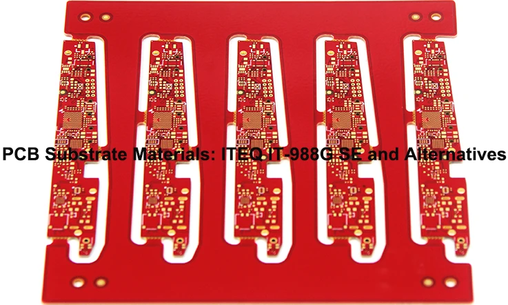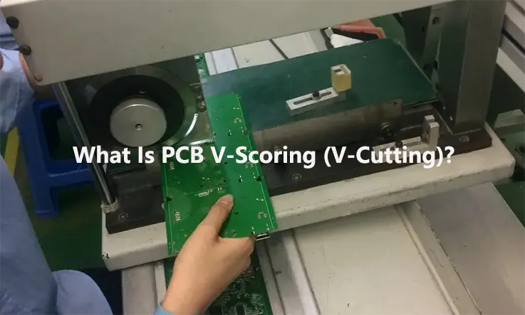
Over time, technological growth reaches ever-greater heights. PCBs have transitioned from a single-layer to a multi-layer design with additional additions. The PCB V Cut is one such example. The V-shaped frame separates the lines connecting the two exteriors. PCB V-scoring is a type of PCB panelization that allows you to put numerous PCBs onto a single manufactured board and then separate them after assembly. It gets its name from the fact that a V-shaped groove is cut into the top and bottom of the PCB.
The purpose of the V-Scoring is to aid PCB manufacturers in severing the board after creation. To divide the PCB, a V-shaped groove is frequently created using a V-cut scoring device. The round blade of the scoring instrument helps to sever material.
What Is PCB V-Scoring (V-Cut) ?
PCB V-Scoring, also known as V-Grooving or V-Cutting, is the process of cutting a “V”-shaped groove at the top and bottom of a rigid board while leaving a narrow space between the Vees. In the manufacturing of printed circuit boards (PCBs) of stiff materials, including FR4, metal core, PTFE, and CEM, the V-scoring technique has been utilized for many years. But V-scoring Inapplicable to flexible circuits boards.
What Are the Distance Rules When V-scoring ?
A widespread misconception is that the ideal PCB size is one that fits precisely within an 18″ × 24″ CCL sheet. In practice, the PCB manufacturer must allocate a portion of the available sheet area for processing. Work together with your PCB manufacturer to establish the optimal PCB panel for your next project. PCB panelization is a process that your PCB manufacturer should be able to assist with. Occasionally, customers prefer to offer their own PCB panels.
V-Scoring Rules:
● The V-cut edg is 3mm.
● The V-Cut min spacing between boards is 2mm.
● The Spacing between the V-scoring line and outline keeps at 0.35mm.
● We recommend board thickness of the V-scored board is 0.6mm at least.
● V-scoring line must be straight and have to be a vertical and horizontal line.
● Minimum PCB size for V-scoring is 60 x 45mm,maximum size is 600mm*450mm.
When you’re V-scoring, it’s helpful to be aware of the distance criteria, as each project will be slightly different. Following these guidelines will help you prevent PCB burring. To prevent traces, pads, and metal layers from being damaged when separating subassemblies at the V-scores, you will need to follow different distance regulations according on the thickness of your PCB.
Contact JarnisTech or whoever your PCB layout engineer is if you are unsure about what the best way to score your PCB is or if your specific PCB does not fit into the distance rules that are provided below. They will be able to assist you in getting the most out of your PCB and will be able to answer any questions you may have.
| Material Thickness | Copper to V-Score | Copper to Routing | SMD Pads |
| 0.80mm | 0.40mm | 0.25mm | 20% |
| 1.00mm | 0.40mm | 0.25mm | 20% |
| 1.55mm | 0.50mm | 0.25mm | 20% |
| 2.00mm | 0.60mm | 0.25mm | 20% |
| 2.40mm | 0.70mm | 0.25mm | 20% |
| 3.20mm | 0.80mm | 0.25mm | 20% |
V-Scoring Equipment
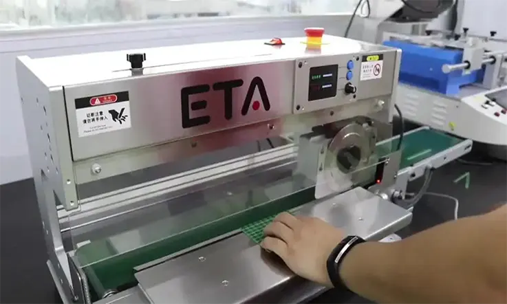
At JarnisTech, we have the most cutting-edge V-scoring equipment available, complete with programmable blades. We are able to program the blades so that they will detach themselves from the panels in the desired location. Because mistakes in jump-scoring can have an effect on the quality of constructed PCBs, we have knowledgeable staff members who are familiar with how to jump-score correctly.
It is essential to properly time the jump-scoring process since allowing the blades to cut into the waste rails could cause the panels to become weakened, which would then cause problems with separation before assembly. If, on the other hand, the blades jump too early, this can cause the V-scoring depth to be reduced, which in turn makes it more difficult for the assembler to separate individual boards from the array.
Jump Score
The option for jump scoring is utilized much less frequently, however it may on occasion be required. The blade comes to a stop before reaching the end of the PC boards, therefore it does not finish recording a score that is continuous from one end of the array to the other. During the process of assembly, this enables a considerably more rigid array to be created.
Why Does a PCB Need V-score ?
Scoring is most commonly utilized in situations in which it is necessary to group a collection of circuit boards for the purpose of making the assembly process more effective. Scoring the printed circuit boards (PCBs) has the idea and aim of creating a sturdy structure for the assembly process that enables you to apply little pressure and separate the boards that have been assembled. This structure is the goal of the scoring process.
PCB V-scoring is done so that board space can be utilized more effectively, and manufacturing costs can be cut by producing multiple identical PCBs on a single manufactured board. This is accomplished by providing the manufacturer with a format for the final board that is more user-friendly for them. You can also add two or more related circuits on the same assembly in order to make the sub-assembly process more efficient in the future.
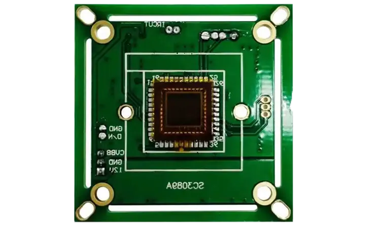
Correct scoring enables the client, engineer, or technician to safely extract sub-PCBs from the manufactured PCB. This effectively increases the number of PCBs.
The ability to V-score PCB confers a significant amount of value on either you or the person who has hired you. The ability to easily V-score a circuit board not only helps save time and money, but it also makes it possible to simply separate individual components from an assembled whole.
V-scoring a printed circuit board (PCB) enables you to treat the entire circuit board as if it were a single board during the process of assembling a PCB. This gives you more flexibility and efficiency. After that, you will be able to place components on every part of the board in a single pass. When you have all of the components placed where you want them, you can then split the boards at the “vees” that you formed earlier. This will make the process of assembly significantly more cost-effective and time-efficient.
Disadvantages of V-Scoring
● Poor scoring due to dull blades.
● Not suitable for low-tolerance PCBs.
● Difficulty in breaking individual parts from the array.
It may be difficult for the assembler to separate individual components from the array if the two grooves on the printed circuit board (PCB) are not sufficiently deep or if they are not properly aligned. Because of this, the stresses that are applied to the assembly might result in a haloing at the dividing edge. It is possible that this could cause the PCB laminate to crack in such a way that the separation will take place outside of the v-scoring channel, which would result in uneven fractures along the board edge.
When the cutting blades of the v-scoring equipment become dull, the outcome can be an offset v-score or extra material between two portions of the board. This results in the separation of individual boards being both uneven and difficult.
Even while the surplus material that is left at the margins of boards that have been split by v-scoring does not have a significant impact on the fitting process, boards that have an extremely low tolerance for unit fit may experience difficulties.
For all your PCB needs, including V-scored PCBs, contact JarnisTech. We are one of China’s foremost PCB makers. We have over two decades of expertise delivering creative PCB fabrication services utilizing the most advanced technology and equipment. Conforming to RoHS (Restrictions on the Use of Certain Hazardous Substances) directives, we adhere to stringent quality requirements. We can meet the diverse PCB prototype and production needs of our customers, from the simplest to the most complicated boards. For additional information, please contact us at [email protected] or 0086/0755-23034656.
V-scoring: How is done ?
One-third of the board thickness is removed from the top, and the remaining one-third is removed from the bottom zone between boards. The remaining one-third of the thickness is what ensures that the boards will remain linked to one another. If the panel is made entirely of PCBs, the material is removed solely from the top or bottom side.
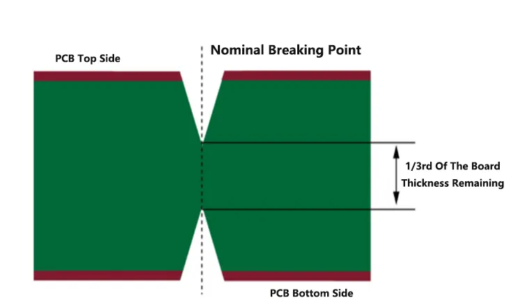
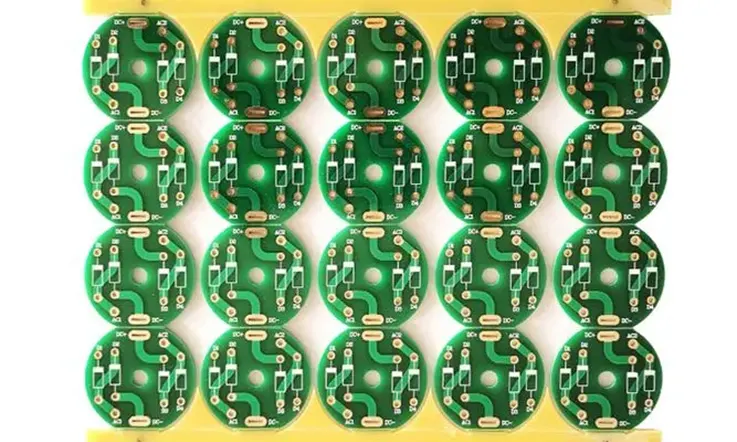
In order for V-scoring to be performed, the shape of the circuit boards must be either rectangular or square. It is not possible to use this method on panels that have a shape that is different from these two options.
V-Scoring PCB Board Procedure
To prevent making incorrect cuts, the V-cutting technique needs to be carried out with extreme caution. The aftereffect of incorrect cutting could be the waste of time, materials, and energy. Because of this, a few fundamental steps are necessary in the procedure regardless of the kind of cutting tools that are employed.
The steps include:
● Use of appropriate safety gear in the correct manner. (Hand gloves, nose mask, and safety goggles). They will provide protection against injuries resulting from inhalation of fumes as well as damage caused by particles.
● Check the measurement to make sure you don’t make any mistakes with the cutting.
● Ensure proper alignment.
● Finally cut into the desired dimension.
Depanelization of V-scored PCB panels
The following procedures can be used to depanelize circuit board panels that have been V-scored:
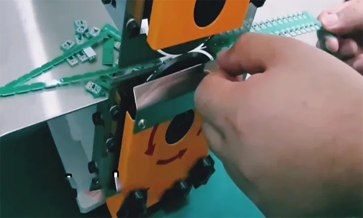
● Pizza cutter: This blade, which can rotate with or without an electric motor, resembles a pizza cutter. It is occasionally held in place by a fixture to ensure proper alignment with the V-groove. Out of the panel, the boards are sliced. This strategy is economical and needs little upkeep.
● Saw: A very high feed rate is possible when cutting V-scored panels with a saw blade. One plus is that doesn’t produce much dust.
● Manual hand breaking: Depanelization of V-scored panels can occasionally be accomplished by simply prying them apart by hand. This could put too much strain on the components, which could cause the board to get damaged. For printed circuit boards (PCBs) that contain strain-sensitive components, manual breaking should never be undertaken.
There are numerous methods for panelization, and V-scoring is one among them. The optimal approach for panelizing and depanelizing your PCB relies on the board’s design. Whether your boards are rectangular or square, you can utilize this method.
PCB V-score Compared to Tab Routing PCB Panels
● Edge components: Tab-routing is a solution that is significantly more practical for edge-hanging components.
● Waste material: V-scoring typically results in far less wasted material compared to tab-routing, and as a result, it is more cost effective.
● Shape of the board: V-scoring is suitable for square or rectangular boards, whereas tab routing is suitable for boards with irregular forms.
● Time: The setup for tab routing requires additional time and effort. V-scoring, on the other hand, is an extremely time-efficient method.
● Edge Quality: The use of V-scoring produces rough edges. Again, tab-routing is going to be the better option if edge quality is a primary concern.
Final Thoughts
PCB’s remarkable achievements and adaptability have made the world a brighter place. As the electronic industry’s needs develop and evolve, it adapts to satisfy those needs in a timely manner.
Your level of understanding will rise if you put the advice and details you’ve gleaned from this essay into practice. In addition to that, it will assist you in determining how to cut your PCB to the appropriate dimensions. This, in turn, helps to maintain your relevance within the field of manufacturing and fabricating.
Understanding how to modify your printed circuit board (PCB) to meet your particular requirements is a crucial component of developing new technologies. PCB V-Scoring gives you the ability to do this on your own, but if you need help turning your vision into a reality, please contact us. We are a PCB manufacturing and Assembly factory in China, and we provide turnkey PCB service from components source to PCB Fabricate to assemble, as well as fast delivery time and high quality products to get more and more trust from our god customers.
Related Posts:
1. What Is PCB Etching and How to Make a perfect PCB Etching?
2. The Best PCB Panelization Guide
3. The Importance of 3D Printed PCBs in Modern Electronics Production
4. Understanding PCB Delamination: A Comprehensive Guide
5. The Best Backplane Printed Circuit Boards Factory
6. An Overview of Through-hole Technology (THT)
7. Detail Talk Surface Mount Technology
8. PCB Clone : Copy Your Printed Circuit Board
9. PCB Drilling: Definition, Technology Types and Process
10. Castellation PCB Fabrication: Castellated Hole (Plated Half Hole) Technologys Why So Important

