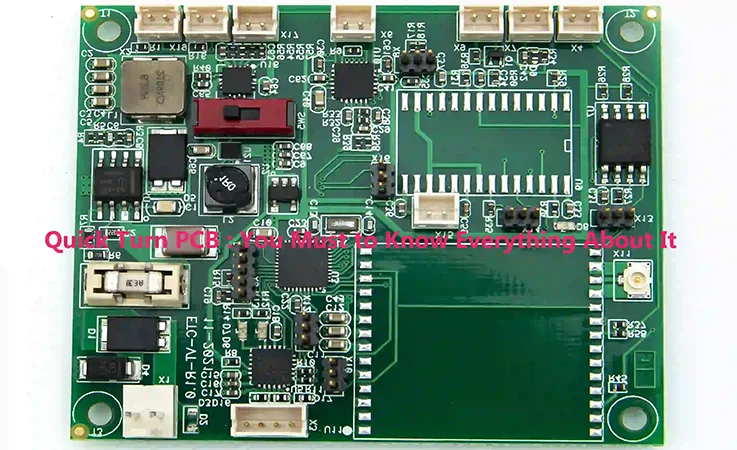
Introduction:
The Growing Demand for Quick Turn PCB in Modern Electronics
The landscape of electronics manufacturing has evolved significantly over the past decade. What was once a slow and cumbersome process involving lengthy production cycles and high costs has now been revolutionized by Quick Turn PCB services. This shift is driven by the ever-increasing need for companies to get their products to market faster while maintaining a high standard of quality. Whether you’re a seasoned electronics manufacturer, an engineer, or a designer, understanding how Quick Turn PCB can streamline your prototyping, assembly, and ultimately speed up your time-to-market is essential.
Quick Turn PCB services offer a solution to an age-old problem: reducing the time it takes to transition from design to prototyping and from prototyping to production. This process is now more efficient, cost-effective, and accessible, allowing companies to stay competitive in an industry that demands constant innovation.
The Changing Landscape of PCB Manufacturing: Why Quick Turn PCB is the Answer?
PCB manufacturing is no longer about just producing the physical circuit boards. It’s about delivering a fast, reliable, and cost-effective solution that aligns with the demands of modern electronics. We today are faced with shorter product lifecycles, more complex designs, and a growing need for rapid iteration. Quick Turn PCB provides a way to address these challenges by drastically reducing lead times, ensuring that prototyping is completed in a matter of days rather than weeks.
This article will explore how Quick Turn PCB services help you accelerate the entire process — from design validation through to prototyping and final assembly — ensuring that your product reaches the market in the fastest time possible without sacrificing quality.
The Quick Turn PCB Manufacturing Process
The process of Quick Turn PCB manufacturing is highly specialized and optimized for speed without compromising quality. For us to deliver prototypes in record time, a combination of advanced technologies, efficient workflows, and smart material choices must be employed. Let’s explore the steps involved in the Quick Turn PCB production workflow, technologies that enable rapid manufacturing, and how selecting the right materials can further optimize turnaround times.
The Quick Turn PCB Production Workflow
The Quick Turn PCB production process is all about taking a design from a sketch to a fully functional, tested circuit board.. It’s a tightly coordinated workflow where each step builds on the last, ensuring that the design is brought to life quickly and efficiently. In this section, we’ll break down each phase and explain how manufacturers ensure speed without sacrificing quality.
The first step in the process is design file preparation. After receiving the design files (Gerber or ODB++), we will conduct checks to ensure that the design can be manufactured efficiently. Then, materials are chosen, fabrication is carried out, and finally, components are placed and soldered. Throughout this process, automated technology and precise manufacturing techniques are utilized to minimize errors and reduce production time.
| Phase | Duration | Key Process | Tools & Technology |
| Design File Preparation | 4-6 hours | File check, DFM (Design for Manufacturability) | CAD Tools, DFM Software |
| Material Selection | 2-4 hours | Choose materials based on design requirements | Material Database, FR4, Rogers |
| Fabrication | 24-48 hours | PCB drilling, etching, and lamination | Laser Drilling, Etching Machines |
| Assembly | 12-24 hours | Component placement and soldering | SMT, Automated Assembly |
| Testing & Quality Check | 4-6 hours | Automated electrical testing and inspection | Automated Optical Inspection, ATE |
| Final Delivery | 24 hours | Packaging and shipment | Packaging Systems, Courier Services |
The entire Quick Turn PCB process can often be completed within 48 to 72 hours, depending on the complexity of the design and the materials used. Let’s now dive deeper into the technologies that make this possible.
Key Technologies Enabling Quick Turn PCB
To achieve quick turnaround times, we rely on a variety of advanced technologies that not only speed up production but also ensure precision. These technologies are designed to streamline workflows and reduce the chances of human error, which could lead to delays.
The core of modern Quick Turn PCB production lies in the combination of Surface-Mount Technology (SMT), automated assembly systems, and advanced CAD tools. These technologies work hand in hand to speed up the manufacturing process while maintaining precise accuracy.
SMT (Surface-Mount Technology) in Quick Turn PCB-
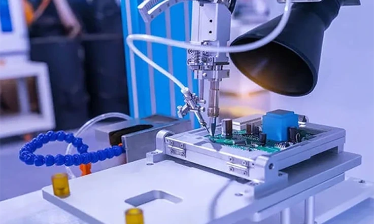
Surface-Mount Technology (SMT) is one of the most important technologies in Quick Turn PCB manufacturing. Unlike through-hole mounting, SMT places components directly on the surface of the PCB, which allows for higher component density and faster production times.
The advantage of SMT is that it enables automated assembly, where machines place components on the PCB, and reflow soldering is used to secure them. With this process, hundreds or even thousands of components can be placed and soldered onto a PCB in a very short amount of time.
| Component Type | Placement Time (per 1000 components) | Assembly Method | Equipment Used |
| Resistors | 20-30 minutes | Surface Mount | Pick and Place Machine |
| Capacitors | 30-45 minutes | Surface Mount | Pick and Place Machine |
| ICs (Integrated Circuits) | 45-60 minutes | Surface Mount | Automated Soldering Machines |
| Other SMT Components | 15-20 minutes | Automated Placement | Reflow Soldering Oven |
The table above illustrates the time efficiency of using SMT for component placement. As we use automated pick-and-place machines, we can achieve high accuracy and speed, ultimately contributing to the quick turnaround time required for prototypes.
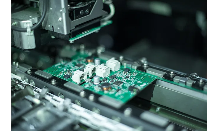
Automated PCB Assembly-
Another cornerstone of Quick Turn PCB is automated PCB assembly. By automating processes like component placement, soldering, and inspection, we reduce the risk of human error and increase the overall speed of production.
Automated systems for PCB assembly typically include pick-and-place machines, wave soldering machines, and automated optical inspection (AOI) systems. These systems can process PCBs faster and with higher precision than manual assembly, allowing us to meet tight deadlines for rapid prototyping.
| Assembly Process | Manual Time (hours) | Automated Time (hours) | Time Savings |
| Component Placement | 4-6 hours | 1-2 hours | 75% faster |
| Soldering | 4-6 hours | 1-2 hours | 70% faster |
| Inspection | 3-4 hours | 1 hour | 75% faster |
The table clearly shows how automated PCB assembly drastically reduces the production time for each assembly stage, allowing us to meet Quick Turn PCB timelines with greater ease and efficiency.
CAD Tools: Precision and Flexibility for Design-
The final technological component in Quick Turn PCB is CAD (Computer-Aided Design) software. Our engineers rely on CAD tools to design and simulate PCBs before moving into fabrication. These tools allow designers to visualize the final product, make adjustments, and even run simulations to test for signal integrity and thermal dissipation issues.
For Quick Turn PCBs, the advantage of using CAD tools is their ability to run Design for Manufacturability (DFM) checks. These checks help identify potential problems early in the design process, ensuring that the board can be manufactured quickly and cost-effectively.
| Design Stage | Time with DFM Checks (hours) | Time without DFM Checks (hours) | Time Savings |
| Design Review | 1-2 hours | 4-6 hours | 50-60% faster |
| Prototyping & Simulation | 2-3 hours | 6-8 hours | 60% faster |
We can see how DFM checks integrated into CAD tools help speed up the entire design process by identifying design flaws before they go into production. By catching potential errors early, we can avoid costly delays that might otherwise result in rework or redesigns.
Material Selection for Quick Turn PCB
The choice of materials used in Quick Turn PCB manufacturing directly impacts both the speed and cost of production. We often opt for materials that allow for faster processing without compromising the PCB’s performance. In this section, we’ll discuss how selecting the right materials can streamline the production process and ensure the best results.
While FR4 remains the most commonly used material for Quick Turn PCBs, there are several other materials available that might be better suited for specific applications. These materials vary in thermal conductivity, electrical properties, and flexibility, which can affect the overall performance of the board.
FR4: The Standard Material for Quick Turn PCB-
FR4 is the go-to material for most Quick Turn PCB projects due to its balance of affordability, availability, and performance. It’s a glass-reinforced epoxy laminate that offers excellent electrical insulation properties and high mechanical strength.
| Material Type | Thermal Conductivity (W/m·K) | Dielectric Constant | Availability (Days) |
| FR4 | 0.3-0.4 | 4.4-5.0 | 2-3 days |
| Rogers | 0.5-0.8 | 2.2-3.0 | 5-7 days |
| Flexible PCBs | 0.2-0.3 | 3.0-3.5 | 4-6 days |
FR4 is highly available and can be processed quickly, which is good for Quick Turn PCB manufacturing. However, for applications requiring higher frequencies or thermal management, we may opt for Rogers materials or flexible PCBs, which offer superior electrical performance and thermal conductivity but may require a longer production lead time. Understanding these material properties and selecting the right one for each specific application can significantly impact both performance and turnaround time.
Rogers Materials: For High-Frequency Applications-
Rogers materials, such as Rogers 4003 and Rogers 4350, are designed for high-frequency applications, making them best for industries like telecommunications and automotive. These materials have lower dielectric loss and lower dissipation factor, making them optimal for high-speed, high-frequency designs.
While they are more expensive than FR4, the improved signal integrity and thermal performance justify their cost for specialized applications.
| Material Type | Thermal Conductivity (W/m·K) | Loss Tangent | Cost (per sqm) |
| FR4 | 0.3-0.4 | 0.02-0.03 | $5-$10 |
| Rogers 4003 | 0.6 | 0.002 | $20-$30 |
| Rogers 4350 | 0.7 | 0.003 | $25-$35 |
The table above compares FR4 with Rogers materials. Rogers materials are more expensive but offer better signal integrity, particularly for high-frequency circuits. For Quick Turn PCB manufacturing, the use of Rogers materials may extend the production time slightly, but the performance benefits in core applications can outweigh the additional costs.
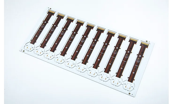
Flexible PCBs: For Complex, Multi-Dimensional Designs-
Flexible PCBs are used in applications where the PCB needs to bend, fold, or fit into tight spaces. This is particularly useful in industries like wearables, medical devices, and consumer electronics. Although flexible PCBs have higher manufacturing costs and longer lead times compared to FR4, their flexibility and versatility make them good for cutting-edge designs.
| Material Type | Thermal Conductivity (W/m·K) | Bending Radius (mm) | Applications |
| FR4 | 0.3-0.4 | NA | Standard applications |
| Flexible PCB | 0.2-0.3 | 4-5 | Wearables, medical devices |
flexible PCBs have lower thermal conductivity compared to FR4 but can be bent into different shapes to fit inside compact devices. These materials are gaining popularity for Quick Turn PCB applications, therefore in the wearable tech market, where space constraints and flexible designs are considerations.
The Advantages of Quick Turn PCB
When developing new electronic products, time-to-market is a competitive factor that can determine a company’s success. Quick Turn PCBs have emerged as a fundamental solution, providing electronics manufacturers with a streamlined process for rapid prototyping, quick design iterations, and cost-effective production. In this section, we’ll explore the significant advantages of Quick Turn PCB, focusing on speed, cost-effectiveness, and design flexibility. We’ll delve into how these factors contribute to faster development cycles and provide a competitive edge for high-tech industries.
Speed and Efficiency: How Quick Turn PCB Saves Time
Many companies choose Quick Turn PCBs to speed up their product development process. These PCBs significantly shorten prototyping cycles, allowing faster testing of new ideas, quicker design iterations, and changes before committing to full production. This shortened timeline is necessary in high-tech industries, where getting products to market quickly can make the difference between staying ahead or falling behind competitors.
Quick Turn PCB not only speeds up the prototyping stage but also enables faster testing and refinement. This reduces the time between the initial design and the final product, ensuring that teams can quickly identify and resolve issues. Here’s a closer look at the specific areas where Quick Turn PCB makes a difference:
●Prototyping Efficiency: A traditional PCB production cycle might take weeks or even months, especially when revisions are required. However, with Quick Turn PCBs, designers can get their prototypes within 48-72 hours. This enables multiple iterations and quick validation of design concepts in a matter of days, not weeks.
●Testing & Validation: Testing early in the development cycle can reveal issues related to signal integrity, thermal management, or electrical performance that would otherwise delay product release. Quick Turn PCBs ensure that we can test and validate designs on a much faster schedule.
| Process | Standard PCB Production (Days) | Quick Turn PCB Production (Days) |
| Design & Prototyping | 7-14 days | 2-3 days |
| Testing & Validation | 10-15 days | 3-5 days |
| Full Production Run | 3-6 weeks | 1-2 weeks |
By enabling faster prototyping and testing, Quick Turn PCB eliminates long delays, allowing us to meet tight deadlines. This quick turnaround time is necessary for industries that need to launch products fast and keep up with changing market demands. With a quicker process, our teams can test designs, make adjustments, and move forward without waiting, helping us stay ahead of competitors.
Cost-Effectiveness of Quick Turn PCB
Beyond speed, Quick Turn PCB offers substantial cost savings. In traditional PCB manufacturing, delays or errors in the design process often result in significant financial losses due to extended lead times, material waste, and rework. Quick Turn PCBs help mitigate these issues by allowing for quicker turnaround times, reducing the likelihood of expensive delays.
1.Reduced Delays: Every delay in production or testing can lead to added costs. Quick Turn PCBs streamline this process by providing rapid prototyping and quick rework cycles. Companies can deliver prototypes in days, which translates into less time spent on iterations and adjustments.
2.Lower Production Costs: For low-volume, high-quality prototypes, Quick Turn PCBs help reduce the unit cost by eliminating long setup times and enabling us to focus on precision assembly without incurring excessive overheads. This is particularly beneficial for businesses that need a limited number of boards but require high-quality performance.
3.Lower Waste: Using Quick Turn PCBs means we are producing fewer unnecessary prototypes and revisions, reducing waste in terms of time, materials, and resources.
| Factor | Traditional PCB Manufacturing | Quick Turn PCB Manufacturing |
| Production Time | 2-3 weeks | 48-72 hours |
| Prototype Cost (Low Volume) | $200-$500 | $100-$250 |
| Material Waste | High | Low |
This table demonstrates how Quick Turn PCBs are more cost-effective than traditional PCB manufacturing methods, especially for low-volume runs. we can spend less on production while still achieving the precision and functionality required for complex designs.
Design Flexibility and Iteration
In today industries, product designs often evolve rapidly based on new market demands or testing feedback. Quick Turn PCBs allow us to adapt and iterate our designs quickly, ensuring that the final product meets the desired specifications while also enabling our engineers to respond to issues as they arise.
One of the greatest advantages of Quick Turn PCB is its ability to support rapid design iterations. Therefore, our designers can quickly refine their PCBs without waiting for weeks or months between revisions. This flexibility is particularly advantageous when:
●Refining Design Features: We can tweak components, change layouts, or test different materials based on real-world feedback, shortening the development timeline.
●Validating Changes: After receiving feedback or discovering issues during the initial tests, we can make rapid updates to the design and validate these changes without delay.
| Design Change | Traditional PCB Cycle (Weeks) | Quick Turn PCB Cycle (Days) |
| Component Placement | 2-3 weeks | 1-2 days |
| Layout Adjustments | 3-4 weeks | 1-3 days |
| Material Modifications | 2-3 weeks | 1-2 days |
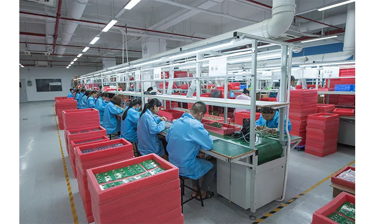
Quick Turn PCB Assembly and Testing
For Quick Turn PCB projects, assembly and testing are where the rubber meets the road. A design may look perfect on paper, but it’s the PCB assembly and rigorous testing that determine if it works in real-world conditions. As speed is a core factor in Quick Turn PCBs, these stages need to be just as swift, efficient, and precise. This section highlights the aspects of PCB assembly, the various testing methods, and the turnkey solutions that drive the fast-paced development cycles of Quick Turn PCB projects.
The Importance of PCB Assembly in Quick Turn Projects
In Quick Turn PCB manufacturing, speed is everything, and the PCB assembly phase is where quickness truly counts. Whether it’s for a prototype or a limited-run product, minimizing delays during assembly ensures that design-to-delivery timelines stay on track. The faster you assemble your PCBs, the faster you can test, refine, and launch them. Without efficient assembly processes, you risk throwing off your entire project timeline.
SMT Assembly vs. Through-Hole Technology-
The most widely used methods of PCB assembly are Surface-Mount Technology (SMT) and Through-Hole Technology (THT). Each of these techniques serves a specific purpose in Quick Turn PCB manufacturing. Understanding how they differ can help streamline the production process, boosting both speed and performance.
●SMT Assembly: SMT assembly is the backbone of modern PCB assembly. It involves mounting components directly onto the surface of the PCB, which allows for higher component density and better performance in smaller form factors. SMT technology is faster and more automated, making it the go-to option for Quick Turn PCB projects where speed and precision are necessary.
●THT Assembly: Through-Hole Technology (THT) involves inserting component leads through holes in the PCB and soldering them on the opposite side. While THT components tend to be bulkier and slower to assemble, they are better suited for applications requiring high mechanical strength and reliability, such as power supplies or connectors.
By combining SMT assembly with THT assembly where needed, we can strike a balance between speed and performance in their Quick Turn PCB projects. The ability to quickly assemble prototypes using SMT while incorporating THT components for durability helps reduce overall turnaround times.
| Assembly Type | Assembly Time (Typical) | Speed Efficiency | Best Used For |
| SMT | 2-4 hours | High | High-density, small form-factor boards |
| THT | 6-12 hours | Moderate | Power components, connectors |
| Mixed (SMT + THT) | 6-8 hours | High | Applications requiring both speed and durability |
PCB Testing: Ensuring Quality in Quick Turn Prototyping
When working with Quick Turn PCB prototypes, testing is the final step before moving to full production. In the fast-moving world of product development, getting your PCB design validated quickly is a must. Testing not only makes sure the product works, but it also catches any potential issues in the design, manufacturing, or materials early. The quicker you spot problems, the quicker you can fix them, making sure the product gets to market on time.
Electrical Testing: Catching Issues Early-
Electrical testing plays a significant part in Quick Turn PCB testing. Automated methods are used to detect issues such as signal integrity, voltage fluctuations, or current leakage, ensuring that the design meets electrical standards. By running tests like continuity checks or short-circuit tests, we can verify that each PCB operates correctly before proceeding to more advanced stages of testing.
Functional Testing: Real-World Evaluation-
Once the electrical tests are passed, functional testing kicks in. This involves testing the PCBs under the conditions they’ll experience in the real world. For instance, in a wearable tech PCB, functional tests might include testing for heat resistance, signal transmission accuracy, or battery life. These tests ensure that the PCB not only functions but performs well under load.
Durability Testing: Stressing the Design-
Durability testing pushes your Quick Turn PCBs to their limits. Whether it’s thermal cycling, vibration tests, or shock testing, durability tests simulate the harsh environments that the product may face. By conducting these tests early in the prototyping process, we can refine the design, making it more reliable and rugged before full production.
| Test Type | Duration (Typical) | Purpose |
| Electrical Testing | 1-3 hours | Verifies electrical integrity |
| Functional Testing | 2-6 hours | Tests real-world performance |
| Durability Testing | 4-12 hours | Ensures product longevity and reliability |
Automated PCB testing tools help ensure a higher level of reliability and accuracy, reducing human error and improving consistency across multiple units. This increases the quality of Quick Turn PCBs, ensuring they meet industry standards and customer expectations.
Turnkey PCB Assembly Services for Quick Turn Projects
For Quick Turn PCB projects, turnkey services are a major advantage. When a single provider handles everything from design to prototyping to testing and assembly, the entire process becomes streamlined and more efficient. Turnkey PCB assembly eliminates the need for customers to juggle multiple suppliers, reducing coordination overhead and speeding up the production timeline.
What’s Included in a Turnkey Solution-
A turnkey solution offers a comprehensive, one-stop-shop for all your PCB needs. Here’s what you get when you opt for a turnkey service:
●Design Services: Expert PCB designers work with you to optimize your design for speed and manufacturability.
●Prototyping: Get quick prototypes based on your design specifications, allowing you to test and iterate in a short amount of time.
●PCB Assembly: Whether it’s SMT or THT, the assembly process is handled quickly and efficiently.
●Testing & Quality Control: Ensure that your Quick Turn PCBs pass all the necessary tests, from electrical to functional and durability testing.
The Benefits of Turnkey Solutions-
With a turnkey PCB solution, your team can focus on innovation while the manufacturer handles the logistics. You’ll benefit from:
●Reduced Lead Time: By consolidating multiple steps with a single provider, you reduce the delays associated with multiple suppliers or vendors.
●Increased Efficiency: A single provider means fewer mistakes, less back-and-forth communication, and better overall project management.
●Cost Savings: With a turnkey solution, you avoid the administrative overhead of managing multiple vendors, ultimately saving on costs.
| Turnkey Service Stage | Average Time (Days) | Benefits |
| Design & Prototyping | 3-5 days | Quick iteration of designs and prototypes |
| PCB Assembly | 2-4 days | Efficient assembly, low error rate |
| Testing & Quality Control | 1-3 days | Accurate testing, quick turnarounds |
By combining all of these services under one roof, turnkey solutions make Quick Turn PCB projects not only faster but also smoother and more cost-effective.
Best Practices for Quick Turn PCB Design
Designing Quick Turn PCBs comes with its own set of challenges. As PCB manufacturer, our goal is always to get from concept to prototype as quickly as possible, while maintaining the highest quality. The good news is that by following specific design best practices, the process can be streamlined. This section will dive into core practices that ensure your Quick Turn PCB designs are manufacturable, error-free, and ready for fast production. We’ll also cover the best tools that can help speed up the design process, and discuss strategies to avoid common design mistakes.
Design for Manufacturability (DFM) in Quick Turn PCB
When it comes to Quick Turn PCB design, the goal is not just to create a functional prototype but to create one that can be easily and efficiently manufactured. This is where Design for Manufacturability (DFM) comes in. DFM focuses on making sure your designs are optimized for production, which minimizes the potential for delays and costly reworks.
DFM Guidelines for Quick Turn PCB Design-
A Quick Turn PCB design that is DFM-compliant is easy to manufacture, reducing production time and costs. The design should adhere to the following key guidelines:
●Component Placement: Place components strategically to reduce trace lengths and minimize routing complexity. This not only speeds up the manufacturing process but also optimizes signal integrity.
●Clearance and Spacing: Ensure adequate spacing between components, pads, and traces. Too-tight placements can increase the risk of manufacturing errors, such as short circuits or incomplete soldering.
●Via Sizes: Minimize the number of vias and their size, as excessive vias can increase manufacturing time and costs. Try to design your board with minimal layers, if possible.
●Trace Width and Impedance Control: Ensure your trace widths and impedance are designed according to the manufacturer’s capabilities. This ensures the design is manufacturable without unnecessary changes.
By following these guidelines, you can ensure that your Quick Turn PCB will not only meet performance requirements but will also be fast-tracked through the manufacturing pipeline, allowing you to accelerate your time-to-market.
| Design Element | Best Practice | Impact on Quick Turn PCB |
| Component Placement | Place components with minimal routing complexity | Faster assembly and fewer errors |
| Clearances | Ensure minimum clearance for pads and traces | Reduced risk of manufacturing defects |
| Via Size | Limit via size and count | Faster production and reduced costs |
| Trace Width | Adhere to the manufacturer’s capabilities | Increased manufacturability and reliability |
Choosing the Right PCB Design Software for Quick Turn Projects
The design software you choose for Quick Turn PCBs can have a massive impact on both the speed and quality of your design. With the right EDA PCB design tools, you can automate many tasks, reduce errors, and ensure that your designs are production-ready.
Popular Design Tools for Quick Turn PCB Projects-
Several PCB design software options are available today, each with its own strengths and capabilities. Here’s a breakdown of the most popular ones:
●Altium Designer: Known for its powerful CAD tools and comprehensive DFM features, Altium Designer is a go-to choice for many engineers. It provides advanced features like 3D visualization and signal integrity analysis, making it best for complex Quick Turn PCB projects.
●Eagle: A more affordable option, Eagle is perfect for low-volume projects. It’s widely used for hobbyists and startups, thanks to its intuitive interface and the availability of an extensive library of components.
●KiCad: An open-source PCB design software, KiCad offers a great alternative to the more expensive tools. It includes a full suite of CAD tools and is capable of handling complex designs for Quick Turn PCBs.
By integrating DFM checks into your chosen software, you can automatically detect potential design issues that could slow down the manufacturing process, allowing you to make adjustments before the design even goes to production.
DFM Integration for Speedier Designs-
Many of today’s PCB design software tools integrate DFM checks directly into the design process. These tools automatically flag any potential manufacturing issues, like small component pads or tight clearances, ensuring your design is optimized for production from the start.
By leveraging CAD integration and DFM tools, you can save time and reduce errors, ensuring that your Quick Turn PCBs stay on track and are ready for manufacturing without unnecessary delays.
| Design Tool | Key Feature | Benefit for Quick Turn PCB |
| Altium Designer | 3D Visualization & Signal Integrity | Reduced design errors and reworks |
| Eagle | Affordable & User-Friendly | Cost-effective for low-volume projects |
| KiCad | Open-Source with Full Features | Free and efficient for complex designs |
Minimizing Errors in Quick Turn PCB Design
Designing Quick Turn PCBs is a fast process, but speed shouldn’t come at the cost of accuracy. Even the smallest design errors can lead to delays in production, rework, and missed deadlines. By focusing on minimizing design mistakes and implementing the best practices, you can ensure that your designs are not only fast but also error-free.
Common Design Mistakes to Avoid-
When designing Quick Turn PCBs, there are a few common mistakes that we often make, leading to delays in production:
●Inadequate Grounding and Power Planes: Poor grounding or insufficient power planes can cause signal interference, which may not show up until testing. Ensuring that ground planes are continuous and well-laid out is essential to avoid this.
●Overcomplicated Designs: Sometimes, we try to pack too much into a small area. Overcrowding components or adding unnecessary features can increase routing complexity and risk manufacturing defects.
●Failure to Check Design Rules: Each PCB manufacturer has its own set of design rules. Failing to check these rules during the design phase can lead to delays when the board is found to be non-compliant with the manufacturer’s capabilities.
Collaboration with Manufacturers: The Key to Avoiding Mistakes-
One of the best ways to avoid design errors is by collaborating early with the PCB manufacturer – JarnisTech. We can provide feedback on your design, help identify potential issues, and suggest optimizations for faster manufacturing.
Therefore, by ensuring constant communication between the PCB designer and the manufacturer, engineers can spot and fix potential issues long before they become major problems, saving time and money in the long run.
| Common Design Mistake | Impact on Quick Turn PCB | Solution |
| Poor Grounding | Signal interference, failure during testing | Ensure proper ground planes and decoupling capacitors |
| Overcomplicated Designs | Increased routing complexity, delays | Simplify design, minimize components |
| Ignoring Design Rules | Rework, delays in production | Double-check design rules with the manufacturer |
How to Choose the Right Quick Turn PCB Manufacturer
Picking the right Quick Turn PCB manufacturer is one of those decisions that can make or break your project. When you’re racing against the clock and need a high-quality prototype in hand, choosing the right partner becomes a game of inches. Not all PCB manufacturers are cut from the same cloth, so it’s smart to check a few boxes before you pull the trigger. In this section, we’ll take you through the steps of picking a manufacturer that matches your speed, budget, and quality goals. By the end of this, you’ll know how to avoid the wrong turn and get your project on the right track.
Choosing a Reliable Quick Turn PCB Manufacturer
When selecting a Quick Turn PCB manufacturer, there are a variety of factors to keep in mind. Experience, certifications, and production capabilities are all core indicators of a manufacturer’s ability to deliver fast, high-quality prototypes.
What to Look for in a Quick Turn PCB Manufacturer-
When choosing a PCB manufacturer, the first thing you’ll want to look at is their track record with Quick Turn PCBs. A solid history of handling quick turnarounds means they’ve likely got their processes down to a science. A seasoned manufacturer knows how to handle even the trickiest designs without dropping the ball, ensuring that your prototype is ready in no time, without skimping on quality. A little experience goes a long way in making sure the process is as smooth as butter.
When choosing a reliable PCB manufacturer, certifications are worth considering. Certifications such as ISO 9001 for quality management and UL certification for safety show that the manufacturer follows established standards. These certifications ensure that your PCB designs are made to the required quality and can be reliably produced in larger quantities later.
Evaluating a Manufacturer’s Ability to Meet Deadlines-
It’s not just about technical capability—it’s also about timeliness. A consideration when choosing a Quick Turn PCB manufacturer is their ability to meet tight deadlines. Check their production capabilities and ask for previous case studies or testimonials to confirm that they’ve been able to meet quick turnaround times for other customers. Also, make sure they can handle low-volume production runs without sacrificing speed or quality.
| Factor | Why It Matters | How to Evaluate |
| Experience | Ensures manufacturer is well-versed in Quick Turn projects | Ask about their track record with similar designs |
| Certifications | Confirms adherence to industry standards | Verify certifications like ISO 9001, UL |
| Production Capability | Ensures quick and accurate turnaround | Review production times and past performance |
| Deadline Reliability | Guarantees your project gets done on time | Ask for references and check their delivery record |
Evaluating PCB Manufacturer Capabilities for Quick Turn Projects
Once you’ve narrowed down a list of potential manufacturers, it’s time to dig deeper into their capabilities. When evaluating a PCB manufacturer for Quick Turn projects, it’s essential to focus on their prototyping lead times, material handling expertise, and the flexibility they offer when it comes to design changes.
Prototyping Lead Times and Material Expertise-
The prototyping lead time is one of the most important metrics for any Quick Turn PCB manufacturer. The faster they can take your design from concept to prototype, the quicker you can begin testing and refining. Ask for specific timelines and ensure they can deliver prototypes within 48-72 hours for standard projects or even faster if needed.
It’s also essential to evaluate the manufacturer’s ability to work with a wide range of materials. If your design requires flexible PCBs, high-frequency substrates, or other specialized materials like Rogers boards, make sure the manufacturer has the expertise to handle these materials efficiently.
Assessing Production Capacity and Flexibility-
Quick Turn projects often require adjustments or design iterations based on test results or customer feedback. Therefore, a manufacturer who is flexible in terms of design changes and can make quick adjustments without extending lead times is a significant advantage. Look for manufacturers that offer turnkey services, meaning they handle everything from design and prototyping to assembly and testing, all under one roof. This reduces handoff times and streamlines communication, ensuring a smoother project flow.
| Capability | Why It’s Important | How to Evaluate |
| Prototyping Lead Times | Faster prototyping means quicker testing and refinement | Confirm the manufacturer’s ability to meet tight deadlines |
| Material Expertise | Essential for designs that require specialized materials | Ask about their experience with flexible or high-frequency PCBs |
| Flexibility for Design Changes | Ensures quick adaptations if adjustments are needed | Discuss their process for accommodating design changes during production |
| Turnkey Services | Reduces lead time by handling all stages in-house | Inquire about their turnkey services from design to assembly |
Why Choose JarnisTech?
For over two decades, JarnisTech has been the go-to partner for engineers, designers, and assemblers who demand precision and speed in their quick-turn PCB needs. Whether you’re a startup or a large corporation, our in-house capabilities and dedication to excellence have earned us the trust of clients across industries like aerospace, automotive, telecommunications, and more. Our track record of on-time delivery is unmatched, helping our clients stay ahead in the fast-paced, competitive world of electronics development.
We understand that when it comes to quick-turn PCBs, time isn’t just money—it’s the difference between a successful launch and missed opportunities. That’s why we prioritize the fastest, most reliable service in the industry, with rigorous quality control and unmatched customer support every step of the way. At JarnisTech, we stand by our promises, offering a robust satisfaction guarantee. If, for any reason, you’re not completely satisfied with your order, we move quickly to resolve the issue and ensure you’re happy with the results.
Fast and Responsive Communication for Faster Turnarounds
What sets us apart from typical PCB manufacturer is our ability to keep things in-house. We manage the entire PCB manufacturing process under one roof, meaning we’re not just waiting for third parties to relay information—we’re directly available to answer your questions, update you on your order status, and make real-time changes as needed. Whether you’re looking for specific material information, updates on your order, or need urgent adjustments to your project, we’re here for you. Our streamlined communication process means no middlemen, no delays.
Here is our quick turn PCB manufacturing capabilities:
| PCB Layers | Order Quantity (m²) | Fabrication Time | Extra Urgent (Hours) |
| 2 Layers | <1 m² | 4 Days | 48 Hours |
| 1-5 m² | 6 Days | – | |
| >5 m² | 7 Days | – | |
| 4 Layers | <1 m² | 4 Days | 48 Hours |
| 1-5 m² | 6 Days | – | |
| >5 m² | 11 Days | – | |
| 6/8 Layers | <1 m² | 6 Days | 72 Hours |
| 1-5 m² | 8 Days | – | |
| >5 m² | 11 Days | – | |
| 10 Layers | <1 m² | 10 Days | 96 Hours |
| 1-5 m² | 10 Days | – | |
| >5 m² | 15 Days | – | |
| 10+ Layers | <1 m² | 10 Days | 96 Hours |
| 1-5 m² | 10 Days | – | |
| >5 m² | 15 Days | – |
TIP: When prototyping multiple PCBs, you can cut down on costs by consolidating them into a single gerber/drill file set. As long as the combined design fits within our standard panel’s usable space of 10″x16″, we will only be charged you fewer charge as though you had a single unique board. It’s also possible to combine both 2-layer and 4-layer boards, as long as the two internal layers on the double-sided board remain unused. Just keep in mind that the surface finish, mask, and silkscreen colors will be the same for all boards in the set.
A Proven Track Record with Industry Giants
Companies like SpaceX, Honeywell, and Boeing choose JarnisTech because they need a fast, reliable partner that understands the importance of tight timelines in high-tech industries. So, if you’re prototyping the next generation of drones or testing cutting-edge medical devices, you need a manufacturer that can meet your quick-turn requirements without compromising on quality. Our proven track record speaks for itself—delivering boards that meet the highest standards, on-time, every time.
Your Success, Our Priority
At our company, we’re not just about producing PCBs; we’re about creating solutions that contribute to your success. We’re committed to understanding your specific goals and products so we can tailor our services to meet your needs. From the initial consultation to the final delivery, we work closely with you to ensure your project stays on track and on budget.
Sharing the Load with Clear Expectations
At JarnisTech, we believe that open communication and transparency are at the heart of strong partnerships. When working with us, we encourage you to share as much information as possible about your project timeline and desired dock date. This helps us understand your needs and allows us to allocate the right resources to meet your deadlines. We know that the PCB manufacturing process is a part of your product development cycle, and we’re here to make sure it fits smoothly into your overall project schedule.
FAQs related to Quick Turn PCB
1. How fast can a Quick Turn PCB be delivered?
Depending on the complexity and quantity, Quick Turn PCBs can be delivered in as little as 24 to 72 hours for simple designs, with more complex configurations taking up to 10 days.
2. Can Quick Turn PCB handle complex designs?
Yes, Quick Turn PCB can handle both simple and complex designs, though more layers or specialized materials might increase lead times.
3. What is the cost difference between standard and Quick Turn PCB?
Quick Turn PCBs tend to be more expensive due to the expedited manufacturing process, but the added cost is often justified by the speed and efficiency it offers.
4. Can I request design revisions during Quick Turn PCB manufacturing?
Yes, design revisions can be requested during the process, though these might impact delivery timelines depending on the scope and complexity of the changes.