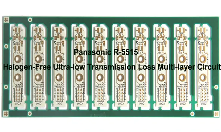
Panasonic’s development of the R-5515 Halogen-Free Material addresses the critical need for a substrate with minimal transmission loss in millimeter wave antennas, particularly for advanced driving support systems (ADAS) and autopilot technologies.
Traditionally, fluororesin substrates have been favored for antenna PCBs due to their low loss characteristics. However, these substrates present challenges in terms of processing and high costs. Panasonic’s R-5515 material offers an alternative solution by leveraging their expertise in resin design and advanced bonding techniques.
With the integration of Panasonic’s resin design technology and low coarsening bonding technology of copper foil, the R-5515 material achieves ultra-low halogen-free transmission loss while ensuring excellent processability. This unique combination allows the material to deliver both low transmission loss and ease of manufacturing, making it an ideal choice for millimeter wave antenna PCBs in ADAS and autopilot systems.
What is Mean for Panasonic R-5515 Halogen-Free Material?
The Panasonic R-5515 Halogen-Free Material is a type of thermosetting resin-based dielectric material specifically designed for use in printed circuit boards (PCBs). It offers insulation and dielectric properties, allowing for improved performance and efficiency in electronic applications.
This material is halogen-free, meaning it does not contain any halogen compounds such as chlorine or bromine. This makes it environmentally friendly and compliant with regulations such as RoHS and REACH.
The R-5515 material has a dielectric constant of 3 and a dissipation factor of 0.002. It also features excellent adhesion strength and is compatible with low-profile copper foils. These properties make it suitable for multilayer PCB constructions and high-frequency circuit boards.
Additionally, the R-5515 material provides good thermal stability, ensuring its performance in high-temperature environments. It also offers dimensional stability, minimizing the risk of warping or distortion in the PCBs.
Overall, the Panasonic R-5515 Halogen-Free Material is a reliable and versatile option for enhancing the insulation and performance of PCBs in various electronic applications.
Panasonic R-5515 Halogen-Free Material: Features
The material being described in the provided characteristics and features is referred to as the fluorine substrate, specifically the Panasonic R-5515 resin material. Here’s a breakdown of its key characteristics:
1.Low Transmission Loss:
The material exhibits low loss of transmission, making it highly suitable for millimeter wave antennas. It enables low loss and high efficiency in millimeter wave antenna applications. This characteristic makes it a versatile option for antenna substrates, potentially replacing other materials.
2.Lowest Loss of Transmission in Thermosetting Resin:
Through resin design technology and bonding techniques, Panasonic has developed this material to achieve the lowest loss of transmission among thermosetting resins. This characteristic enhances its performance in transmitting signals effectively.
3.Great PCB Processability:
The material offers excellent processability for printed circuit boards (PCBs), leading to reduced processing costs. Unlike fluororesin substrates, which require specific equipment for copper plating and hole drilling, this thermosetting resin material can be processed using general PCB equipment. This feature contributes to cost savings in PCB manufacturing.
4.Compatibility with FR4:
The Panasonic R-5515 resin material can be easily formed alongside FR4, a commonly used substrate material for PCBs. This characteristic allows for convenient integration and compatibility with FR4, facilitating the development of multilayer antenna module substrates. The material’s ease of formation supports the miniaturization and cost reduction efforts in wave band modules.
5.Difficulty in Forming with Glass Substrate:
Unlike glass substrate materials, the fluororesin substrate, being a thermoplastic resin, presents challenges in forming simultaneously with the glass substrate. This characteristic implies that the material may not be well-suited for applications that require simultaneous formation with glass substrates.
Overall, the Panasonic R-5515 resin material offers advantages such as low transmission loss, high processability, and compatibility with FR4, making it a valuable option for millimeter wave antenna applications and PCB manufacturing.
Properties of the Panasonic R-5515 Material
The provided general properties of the Panasonic R-5515 material are as follows:
1. Glass Transition Temperature (Tg): The material has a glass transition temperature of 200 degrees Celsius when tested using the DMA (Dynamic Mechanical Analysis) method. Additionally, it has a value of 170 degrees Celsius when tested using the TMA (Thermomechanical Analysis) method. The glass transition temperature indicates the temperature at which the material transitions from a rigid, glassy state to a more flexible, rubbery state.
2. Decomposition Temperature: The material has a decomposition temperature of 410 degrees Celsius, determined through the TGA (Thermogravimetric Analysis) method. This temperature represents the point at which the material chemically decomposes.
3. Coefficient of Thermal Expansion (CTE): The material exhibits different CTE values depending on the axis. For the Z-axis, the CTE is 50 ppm/℃ at α1 and 300 ppm/℃ at α2. For the X and Y axes, the CTE values are in the range of 19-21 ppm/℃ at α1. The CTE indicates how much the material expands or contracts when subjected to temperature changes.
4. Dielectric Constant (Dk): The material has a dielectric constant of 3.06 at a frequency of 14 GHz. The dielectric constant measures a material’s ability to store electrical energy in an electric field. It affects the propagation of electromagnetic waves through the material.
5. Dissipation Factor (Df): The material has a dissipation factor of 0.002 at 14 GHz. The dissipation factor represents the material’s inefficiency in acting as an insulator. A low dissipation factor indicates that the material is highly efficient as an insulating material.
6. Delamination Time (T288): The material has a delamination time of greater than 120 minutes without copper and greater than 20 minutes with copper when subjected to a temperature of 288 degrees Celsius using the TMA method. Delamination refers to the separation of layers in a PCB’s base material. The delamination time indicates the time it takes for the material to delaminate under specific temperature conditions.
These general properties provide insights into the thermal, electrical, and mechanical characteristics of the Panasonic R-5515 material, which are important considerations for its application in various industries.
Applications of the Panasonic R-5515
The Panasonic R-5515 material has several applications due to its specific properties. Some of the applications include:
Millimeter Wave Antenna Printed Circuit Boards:
Millimeter wave antenna printed circuit boards (PCBs) are designed to facilitate the transmission and reception of millimeter wave signals, which operate in the frequency range of 30 GHz to 300 GHz. These PCBs are crucial components in millimeter wave communication systems and are used in various applications such as wireless backhaul, 5G networks, radar systems, and satellite communications. They are specifically designed to handle the high-frequency signals and provide low loss, high efficiency, and precise signal integrity.
High-Speed PCB Transmission:
High-speed PCB transmission refers to the capability of a printed circuit board to transmit signals at high frequencies with minimal loss and distortion. It is essential in applications such as data communication, telecommunication, and high-speed digital systems. To achieve high-speed transmission, PCBs need to be designed with controlled impedance, low signal loss, and effective signal integrity management. Advanced PCB design techniques, such as impedance matching, signal routing optimization, and the use of high-frequency materials, are employed to ensure reliable and efficient high-speed signal transmission.
Wireless Communication:
Wireless communication refers to the transmission of information or data without the need for physical wired connections. It enables the exchange of data over a wireless medium, typically using radio frequency (RF) signals. Wireless communication technologies include cellular networks (such as 5G, 4G, and earlier generations), Wi-Fi, Bluetooth, satellite communication, and various IoT (Internet of Things) devices. PCBs play a crucial role in wireless communication systems, providing the necessary circuitry and components for RF signal processing, modulation, demodulation, amplification, and antenna integration.
Conclusion
With the introduction of the Panasonic R-5515 Halogen-Free Material, the automotive industry has gained a game-changing solution for achieving superior millimeter wave antenna performance. By combining low transmission loss, excellent processability, and cost-effectiveness, Panasonic has addressed the limitations of traditional substrates. As ADAS and autopilot technologies continue to advance, the R-5515 material paves the way for enhanced safety and efficiency in the vehicles of tomorrow. With Panasonic’s commitment to innovation, the future of automotive antennas is brighter than ever.

