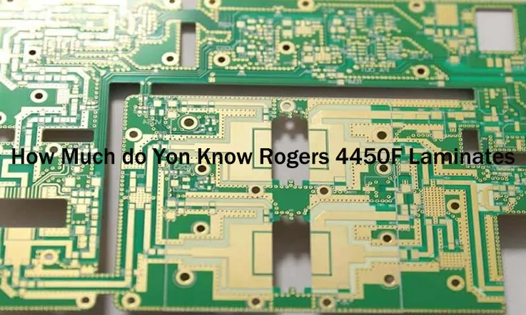
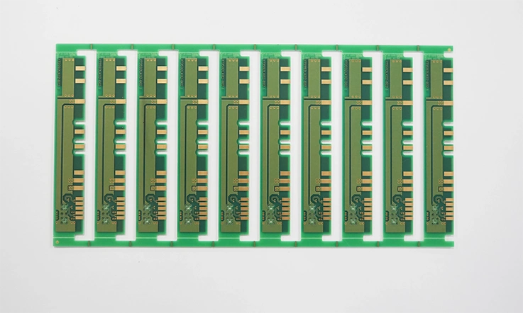
As RF, microwave, and millimeter-wave technologies advance, selecting the right PCB laminate demands precision. Nelco N9000-13 RF has established itself as a go-to material for human tackling 5G infrastructure, radar systems, aerospace electronics, and high-frequency communications. With its low dielectric loss, stable impedance control, and robust thermal reliability, this laminate provides a strong foundation for designs demanding high signal fidelity and long-term stability.
But achieving top-tier performance isn’t just about material selection—it’s about understanding fabrication challenges, cost trade-offs, and advanced stackup configurations. This guide explores the electrical, thermal, and mechanical advantages of Nelco N9000-13 RF, while diving into processing techniques, hybrid stackup strategies, and industry comparisons with materials like Rogers, Taconic, and Isola.
Understanding Nelco N9000-13 RF and Its Impact on High-Frequency PCB Performance
Designing RF and microwave PCBs isn’t just about picking a material off a shelf—it’s about ensuring your design can handle the real-world demands of high-frequency applications. If your PCB laminate can’t maintain signal integrity at GHz-level frequencies, you’ll be dealing with signal degradation, EMI issues, and costly redesigns.
That’s why we are turning to Nelco N9000-13 RF, a laminate that has been making waves in 5G infrastructure, satellite communications, radar systems, and high-speed data applications. But what exactly sets it apart from other laminates in the industry? Let’s break it down.
What Makes Nelco N9000-13 RF Stand Out in the PCB Industry?
If you’ve been in the RF PCB game long enough, you know that not all laminates are built the same. A slight dielectric constant (Dk) variation or an unexpected loss tangent (Df) increase can completely throw off your circuit’s performance.
Precision-Engineered Dielectric Constant Stability-
Nelco N9000-13 RF is produced with more precise Dk control than standard laminates. In high-frequency designs, even the slightest variation in material properties can cause impedance mismatches and phase deviations in RF signals, making precision a necessity at the nanometer level.
| Material | Dielectric Constant (Dk) @ 10 GHz | Loss Tangent (Df) @ 10 GHz | Thermal Stability |
| Nelco N9000-13 RF | 3.00 ± 0.04 | 0.0025 | Excellent |
| Rogers RO4003C | 3.38 ± 0.05 | 0.0027 | Moderate |
| Taconic TLY-5 | 2.22 ± 0.05 | 0.0009 | Good |
| FR4 (Standard) | 4.50 ± 0.15 | 0.0200 | Poor |
What this means for your PCB: If you’re working on 24 GHz radar, mmWave, or high-speed RF applications, you can’t afford unpredictable material behavior. Nelco N9000-13 RF delivers consistency where it matters most.
Optimized Copper Foil and Surface Roughness-
The copper-clad layer on your laminate isn’t just a “nice-to-have”—it’s a main factor in how well your circuit performs. If you’re dealing with excessive copper roughness, you’ll see increased conductor losses, impacting overall efficiency.
Nelco N9000-13 RF uses a low-profile copper treatment, ensuring minimal skin effect losses at mmWave and high-frequency bands.
Real-world impact: A high-speed interconnects manufacturer saw 3 dB less insertion loss simply by switching from a rough copper PCB to a Nelco N9000-13 RF-based design. That’s the difference between reliable performance and scrap-bin disasters.
Why Choose Nelco N9000-13 RF Over Other High-Performance Laminates?
Picking a PCB laminate isn’t about grabbing whatever’s trending—it’s about balancing cost, manufacturability, and electrical performance. While Rogers, Taconic, and Panasonic materials have their strengths, Nelco N9000-13 RF offers a compelling balance that’s hard to ignore.
Cost-Performance Sweet Spot-
Let’s face it: PTFE-based laminates (like Rogers RT/Duroid) perform exceptionally well, but they can be a pain to process. They require specialized drilling, plating, and bonding processes, which can drive up production costs.
Nelco N9000-13 RF, on the other hand, delivers low-loss performance without the need for exotic manufacturing techniques. That means lower scrap rates, easier fabrication, and reduced lead times.
Thermal Performance That Handles the Heat-
Ever dealt with warping or delamination because your PCB couldn’t handle thermal cycling? This is a serious issue for automotive radar, aerospace electronics, and 5G base stations, where temperature swings are the norm.
Nelco N9000-13 RF excels in high-temperature environments—meaning fewer failures, longer product lifespans, and less warranty liability.
Case Study: A defense contractor switched from a Rogers-Teflon hybrid stack-up to a full Nelco N9000-13 RF design, reducing their PCB failure rate by 27% under high-heat conditions.
Key Advantages of Nelco N9000-13 RF for RF and Microwave Applications
If you’re designing PCBs for RF, microwave, or mmWave applications, you need a material that checks all the right boxes. Here’s why Nelco N9000-13 RF should be on your radar.
Low Loss Tangent for Cleaner Signal Transmission-
At high frequencies, even minor signal loss can have a noticeable impact. Nelco N9000-13 RF features an ultra-low loss tangent (Df) of 0.0025, allowing signals to travel with minimal attenuation, even in mmWave bands.
Takeaway: If you’re working on satellite transponders, radar antennas, or 5G backhaul links, lower loss means better efficiency and higher reliability.
Manufacturing-Friendly Without the Hassle of PTFE-Based Materials-
One major headache with PTFE laminates (like Rogers RT5880) is that they require specialized processing techniques—from controlled lamination cycles to plasma etching for via preparation.
Nelco N9000-13 RF sidesteps these issues, offering high-frequency performance in a more fabrication-friendly package.
Case Study: A 5G infrastructure manufacturer cut PCB production costs by 22% by switching from a PTFE-based stack-up to Nelco N9000-13 RF, all while maintaining the same RF performance.
Consistent Electrical Properties Over Temperature and Humidity Cycles-
RF circuits don’t just operate in perfect lab conditions—they have to endure heat, humidity, and mechanical stress. Some laminates suffer from Dk drift under extreme conditions, leading to unreliable impedance control.
Nelco N9000-13 RF offers excellent environmental stability, making it ideal for aerospace, military, and harsh-environment applications.
Nelco N9000-13 RF Electrical Properties: Ensuring Superior Signal Integrity
Designing RF and high-frequency PCBs isn’t just about layout and routing—it’s about ensuring that every signal travels as expected. The wrong material choice can lead to unexpected attenuation, phase shifts, and inconsistent performance.
For engineers working on 5G networks, aerospace communication, satellite systems, and radar applications, a laminate must provide predictable electrical behavior across a wide range of frequencies and environmental conditions. Nelco N9000-13 RF is designed with these applications in mind, offering a combination of low dielectric loss, stable impedance characteristics, and reliable high-frequency performance.
Low Dielectric Loss and Minimal Signal Attenuation with Nelco N9000-13 RF?
When dealing with RF, microwave, and mmWave circuits, energy loss is something that needs to be controlled. A higher loss tangent (Df) means that signals weaken as they travel along traces, reducing efficiency and distorting waveforms.
Understanding Dielectric Loss in High-Frequency PCB Design-
Dielectric loss is the amount of energy absorbed by the PCB material as signals pass through. This absorption converts some of the signal power into heat, leading to degradation over distance. For systems operating at GHz frequencies, even small variations in loss tangent (Df) can affect performance.
How Nelco N9000-13 RF Helps Maintain Signal Integrity-
This material is manufactured with a loss tangent (Df) of 0.0025 at 10 GHz, which means signals experience minimal weakening as they propagate. As a result, it supports longer transmission distances and cleaner waveforms, making it suitable for applications that require high signal fidelity.
Comparing Dielectric Loss Across Common RF PCB Materials-
A variety of RF laminates exist on the market, each with different levels of dielectric loss. Materials with higher Df values can experience increased attenuation, while those with lower Df values allow signals to remain intact over greater distances.
Controlled Impedance and Stability in High-Speed PCB Designs
In RF and high-speed digital designs, maintaining precise impedance values is necessary for reliable performance. Any variation in impedance can lead to reflections, distortion, and unpredictable signal behavior.
Why Impedance Control Matters in High-Frequency PCBs-
High-frequency signals are sensitive to variations in impedance. When impedance fluctuates, signals don’t transition as expected, causing voltage mismatches that can introduce noise and degrade data accuracy.
How Nelco N9000-13 RF Supports Impedance Stability-
●Low variation in dielectric constant (Dk) ensures uniform impedance across all layers
●Consistent electrical properties across a broad frequency range
●Reliable fabrication process compatibility, preventing unexpected impedance deviations
Stack-Up Considerations for Impedance Control-
To achieve stable impedance values, selecting the right layer configuration and trace width is necessary. Nelco N9000-13 RF allows for predictable stack-up designs that maintain impedance uniformity across high-speed signal paths.
Comparing Nelco N9000-13 RF vs. Rogers, Taconic, and Isola Materials
Selecting the right laminate depends on factors such as loss characteristics, processing ease, and manufacturing consistency. While Rogers, Taconic, and Isola all offer high-performance laminates, there are distinct differences in material properties and handling requirements.
Key Factors to Consider When Choosing an RF Laminate-
●Dielectric constant (Dk) stability for consistent impedance
●Loss tangent (Df) characteristics for signal retention
●Thermal performance under varying operating conditions
●Compatibility with standard fabrication processes
Where Nelco N9000-13 RF Fits in the Market-
●Designed to provide low-loss performance
●Compatible with standard PCB manufacturing techniques
●Offers predictable electrical properties across different operating frequencies
Material Property Comparison-
Different RF laminates have unique properties that affect how they perform in specific applications. Some materials are optimized for low loss, while others focus on ease of processing or high-frequency stability.
| Property | Nelco N9000-13 RF | Rogers RO4003C | Taconic TLY-5 | Isola Astra MT77 |
| Dk @ 10 GHz | 3.00 ± 0.04 | 3.38 ± 0.05 | 2.95 ± 0.05 | 3.00 ± 0.04 |
| Loss Tangent (Df) @ 10 GHz | 0.0025 | 0.0027 | 0.0019 | 0.0017 |
| Thermal Performance | Stable | Moderate | Good | High |
| Manufacturing Complexity | Low (Standard Processing) | Medium | Medium | High |
By analyzing these material properties, we can determine which laminate best aligns with the needs of our specific application.
Thermal and Mechanical Advantages of Nelco N9000-13 RF
Designing RF and microwave circuit boards isn’t only about electrical performance. At GHz frequencies, managing heat and maintaining mechanical stability can’t be overlooked. Any shifts in material dimensions due to thermal changes may cause PCB warping, solder joint strain, and unexpected performance variations.
That’s where Nelco N9000-13 RF makes an impact. It offers low thermal expansion, excellent heat dissipation, and robust mechanical strength, making it a solid choice for high-reliability applications such as 5G infrastructure, satellite communication, radar systems, and aerospace electronics.
Let’s break down how it tackles heat management, dimensional stability, and fabrication challenges.
How Nelco N9000-13 RF Enhances PCB Heat Management and Thermal Conductivity?
Thermal buildup in RF and microwave circuits isn’t something you can ignore. High-frequency components, power amplifiers, and dense layouts generate heat, and if a PCB material can’t handle it, expect frequency shifts, signal distortion, and even outright failure.
Understanding Thermal Conductivity in PCB Materials-
Thermal conductivity (TC) refers to how well a material moves heat away from hot components. A higher TC value means better heat dissipation, keeping components within their operating range.
| PCB Material | Thermal Conductivity (W/m·K) |
| Nelco N9000-13 RF | 0.35 |
| Rogers RO4003C | 0.71 |
| Taconic RF-35 | 0.22 |
| Isola Astra MT77 | 0.30 |
While some materials may offer higher thermal conductivity, Nelco N9000-13 RF balances heat dissipation with excellent electrical properties, ensuring low loss and stable impedance.
How This Material Handles Heat Differently-
●Lower Coefficient of Thermal Expansion (CTE): Reduces stress on solder joints and vias
●Stable Dk Across Temperature Changes: Prevents impedance shifts in high-power applications
●High Glass Transition Temperature (Tg): Keeps the board from softening under elevated temperatures
Why Heat Management Matters in RF and Microwave PCBs-
When a 5G base station or satellite transceiver operates under heavy loads, heat can quickly degrade performance. A laminate with poor heat dissipation will cause frequency instability, leading to signal degradation and lost efficiency. Nelco N9000-13 RF helps mitigate this by keeping temperatures in check.
Ensuring Dimensional Stability in RF and Microwave Circuit Boards
A PCB that warps, expands, or shrinks during operation or manufacturing isn’t going to hold up in demanding environments. High-frequency circuits need precision, and even a slight change in dimensions can throw off impedance calculations, making circuits act up in unexpected ways.
How Nelco N9000-13 RF Maintains Structural Integrity-
●Low CTE (Coefficient of Thermal Expansion): Prevents PCB distortion at high temperatures
●Minimal moisture absorption: Reduces environmental impact on electrical properties
●Consistent mechanical strength: Withstands high-speed drilling, plating, and soldering
| Material Property | Nelco N9000-13 RF | Rogers RO4350B | Taconic TLY-5 | Isola I-Tera MT40 |
| CTE (Z-axis, ppm/°C) | 40 | 50 | 30 | 45 |
| Moisture Absorption (%) | 0.02 | 0.06 | 0.01 | 0.04 |
| Tg (°C) | 210 | 280 | 330 | 200 |
Why Dimensional Stability is a Big Deal for RF Engineers-
When fabricating multilayer RF PCBs, variations in expansion or contraction during lamination can misalign layers, affecting impedance. If a material doesn’t stay in shape, we end up with boards that don’t perform like they should. Nelco N9000-13 RF offers a predictable mechanical response, helping to maintain design accuracy.
How to Avoid Board Warping During Fabrication-
●Use proper layer stack-ups to distribute thermal stress
●Ensure correct material handling to prevent moisture absorption
●Control reflow soldering profiles to reduce thermal shock
Processing Challenges and Solutions for Nelco N9000-13 RF Fabrication
Even high-end RF laminates can present challenges during fabrication. Careful handling during drilling, plating, etching, and soldering helps ensure consistent and dependable results.
Common Challenges in Manufacturing Nelco N9000-13 RF PCBs-
●Drilling & Hole Wall Integrity: Some RF materials tend to have rough hole walls after drilling, impacting plating quality.
●Copper Peel Strength: High-frequency laminates often use smoother copper foils to reduce loss, but this can impact adhesion.
●Thermal Expansion Mismatch: Differences between laminate and prepreg materials can cause delamination if not handled correctly.
Best Practices for Fabrication-
●Use high-speed drilling techniques to maintain clean hole walls
●Ensure proper desmear and plasma treatment for strong plating adhesion
●Match laminates with compatible prepregs to minimize expansion mismatches
How Manufacturers Can Get the Most Out of Nelco N9000-13 RF-
PCB manufacturers working with RF laminates need to fine-tune their etching, drilling, and lamination processes to get the best performance. With proper fabrication techniques, Nelco N9000-13 RF delivers the reliability needed for high-frequency applications.
Optimizing PCB Design with Nelco N9000-13 RF for RF and Microwave Performance
Designing high-frequency PCBs isn’t just about picking the right material—it’s about using it correctly. Nelco N9000-13 RF offers advantages in low dielectric loss, signal integrity, and thermal stability, but if layer stackup, transmission line configurations, or isolation techniques aren’t well thought out, even the best material may not perform as expected.
Poor design choices can lead to signal degradation, impedance mismatches, and increased crosstalk—all of which can compromise performance in 5G communication, radar, satellite systems, and other high-frequency applications.
So, how can Nelco N9000-13 RF be used to its full potential? Here are some effective design strategies.
Best Practices for Layer Stackup Using Nelco N9000-13 RF
In high-frequency PCB design, layer stackup defines signal integrity. A poorly arranged layer structure can lead to unwanted losses and electromagnetic interference.
How to Structure an RF PCB Stackup Effectively-
When using Nelco N9000-13 RF for microwave and high-speed digital circuits, consider the following:
●Dielectric layer thickness: Thinner layers reduce insertion loss but may increase crosstalk
●Ground plane placement: Proper reference planes support impedance control
●Balanced layer structure: Prevents warping and uneven etching
A standard 4-layer RF PCB stackup using Nelco N9000-13 RF might look like this:
| Layer | Function | Material |
| L1 | RF signal layer | Nelco N9000-13 RF |
| L2 | Ground plane | Copper |
| L3 | Power plane or RF return layer | Copper |
| L4 | RF signal layer | Nelco N9000-13 RF |
For more complex multilayer designs, additional ground planes can be added to minimize signal coupling and interference.
How Stackup Affects RF and Microwave PCB Performance-
A well-structured stackup delivers:
●Consistent impedance control, reducing waveform distortion
●Lower electromagnetic interference (EMI), improving system predictability
●Better phase consistency, beneficial for radar and high-frequency communications
If the goal is to maintain stability in high-frequency applications, then a carefully arranged layer stackup is necessary.
Microstrip vs. Stripline Configurations with Nelco N9000-13 RF
In RF PCB layouts, signal traces are typically designed as either microstrip or stripline configurations. Each approach influences signal integrity, manufacturability, and cost.
Microstrip vs. Stripline: Which One to Choose?
| Configuration | Advantages | Challenges |
| Microstrip | Easier to manufacture, lower losses | More susceptible to external interference |
| Stripline | Provides better shielding, reduces EMI | More complex fabrication, increased cost |
If EMI reduction is the main concern, stripline may be a better fit, whereas microstrip can be a more practical choice when cost and ease of manufacturing are priorities.
How to Optimize Microstrip and Stripline Layouts with Nelco N9000-13 RF-
●For Microstrip: Keep the ground plane close to reduce radiation
●For Stripline: Maintain a uniform dielectric thickness for impedance consistency
●For Both: Leverage Nelco N9000-13 RF’s low-loss properties to maintain signal strength
If better electromagnetic shielding is needed, stripline is worth considering. On the other hand, if manufacturing simplicity is the focus, microstrip is often the go-to choice.
Reducing Crosstalk and Signal Reflection in High-Frequency PCBs
In high-frequency circuit boards, crosstalk and signal reflection are frequent challenges. Poor routing techniques can result in unintended signal coupling, affecting data integrity.
What Causes Crosstalk in RF PCBs?
Crosstalk typically occurs in high-density layouts, caused by:
●Narrow spacing between signal traces, leading to capacitive coupling
●Improper ground plane arrangements, reducing shielding effectiveness
●Unoptimized return paths, creating unnecessary interference
How to Reduce Crosstalk in Nelco N9000-13 RF PCBs-
●Increase spacing between traces to lower capacitive effects
●Route signal layers perpendicular to each other to minimize interference
●Ensure ground planes are properly placed for better shielding
How to Control Signal Reflection in High-Frequency Circuits-
Signal reflection is mainly caused by impedance mismatches, which can lead to:
●Increased power loss, affecting transmission efficiency
●Data jitter and distortion, impacting system reliability
●Higher insertion loss, leading to reduced performance
Ways to Reduce Signal Reflection-
●Match transmission line impedance with load impedance to prevent signal bouncing
●Use termination resistors to absorb excess energy
●Minimize unnecessary vias and stubs to avoid signal reflections
By utilizing Nelco N9000-13 RF’s consistent dielectric properties, these issues can be better managed.
Fabrication & Processing Guidelines for Nelco N9000-13 RF PCB Manufacturing
Handling high-frequency laminates such as Nelco N9000-13 RF requires an approach that aligns with its material characteristics. Unlike conventional FR4, it responds differently to heat, pressure, and drilling parameters, making it essential to adjust fabrication methods accordingly.
Without the right lamination techniques, drilling strategies, and surface finish choices, manufacturing challenges may arise, affecting PCB durability and signal behavior. For designs incorporating hybrid stackups, where Nelco N9000-13 RF is paired with other materials, attention to processing conditions can help avoid misalignment, delamination, or uneven dielectric performance.
Let’s explore methods that keep fabrication efficient and results consistent.
Lamination and Drilling Techniques for Nelco N9000-13 RF
Working with low-loss laminates means adjusting processing parameters to prevent mechanical stress, resin flow issues, or poor hole quality.
Lamination Considerations for Nelco N9000-13 RF-
The glass transition temperature (Tg) and coefficient of thermal expansion (CTE) of Nelco N9000-13 RF differ from FR4, requiring adjustments to lamination conditions.
●Steady Heating and Cooling: Avoids thermal stress buildup
●RF-Compatible Prepregs: Ensures a strong interface between layers
●Uniform Pressure Application: Reduces thickness inconsistencies
A standard lamination cycle for Nelco N9000-13 RF often follows:
| Step | Temperature (°C) | Pressure (psi) | Time (Minutes) |
| Preheat | 80 – 120 | 50 – 100 | 30 – 60 |
| Full Pressure | 170 – 190 | 250 – 400 | 90 – 120 |
| Cooling | Below 100 | Gradual Release | 30 – 45 |
Drilling Considerations for Nelco N9000-13 RF-
Drilling through fiber-reinforced RF laminates presents challenges, as standard FR4 drilling techniques can result in rough hole walls, resin smear, and dimensional shifts.
Recommended Drilling Settings:
●Drill Bit Type: Carbide tools with diamond-coated edges for extended tool life
●Spindle Speed: 30,000 – 60,000 RPM to minimize material tearing
●Chip Load: Low feed rates (~0.5 – 2 mils per revolution) to reduce mechanical stress
●Entry & Backup Materials: Aluminum entry sheets + phenolic backing boards for better drill accuracy
Adjusting these settings helps maintain hole integrity and prevents defects that could interfere with subsequent plating steps.
Choosing the Right Surface Finish: ENIG, OSP, or Immersion Silver?
The selection of a surface finish impacts soldering consistency, oxidation resistance, and high-frequency behavior. Some finishes perform better than others depending on circuit density, thermal exposure, and storage conditions.
Surface Finish Comparisons-
| Finish | Advantages | Considerations |
| ENIG (Electroless Nickel Immersion Gold) | High corrosion resistance, smooth surface for fine-pitch components | Higher cost, potential for “black pad” defects |
| OSP (Organic Solderability Preservative) | Cost-efficient, environmentally friendly | Shorter shelf life, not suitable for multiple reflow cycles |
| Immersion Silver | Low insertion loss, better RF performance than OSP | Requires careful storage to prevent tarnishing |
Best Fit for Nelco N9000-13 RF Applications-
Selecting a surface finish depends on PCB usage conditions and design priorities:
●For RF circuits with fine-pitch connectors → ENIG
●For cost-sensitive production runs → OSP
●For applications requiring smooth, conductive surfaces → Immersion Silver
Tip: Finishes with high surface roughness can introduce insertion loss variations, affecting high-frequency transmission.
How to Optimize Hybrid Stackups with Nelco N9000-13 RF for Cost Efficiency?
Mixing Nelco N9000-13 RF with FR4 or other laminates allows for cost adjustments while maintaining specific electrical properties where needed. However, hybrid stackups require attention to thermal expansion rates, bonding materials, and mechanical stress distribution.
Factors to Consider in Hybrid PCB Stackups-
●Material Expansion Rates: Mismatched CTE values can cause layer separation
●Prepreg Compatibility: Some bonding materials may not adhere well between different substrates
●Thermal Behavior: Heat dissipation must be evenly distributed to avoid localized stress points
Example Hybrid Stackup for Cost Adjustment-
| Layer | Material | Function |
| L1 | Nelco N9000-13 RF | High-frequency signal layer |
| L2 | FR4 Core | Cost-managed structural layer |
| L3 | Nelco N9000-13 RF | Controlled impedance return path |
| L4 | FR4 Substrate | Mechanical support layer |
Stackup Considerations-
●CTE Alignment: Reduces the risk of warping or stress fractures
●Bonding Methods: Selecting compatible prepregs improves long-term durability
●Heat Exposure Control: Helps maintain dimensional accuracy through multiple soldering cycles
Balancing material selection and processing adjustments allows for manufacturing cost control without performance trade-offs.
Cost Optimization Strategies for High-Performance RF PCBs Using Nelco N9000-13 RF
Manufacturing RF and microwave PCBs requires precise material selection and processing techniques to balance electrical performance, thermal efficiency, and cost considerations. Nelco N9000-13 RF provides low-loss signal transmission and stable mechanical properties, but optimizing fabrication strategies can further improve cost efficiency while maintaining signal integrity.
By adjusting stackup configurations, copper thickness, and drilling methods, we can develop more streamlined production processes, making high-frequency designs more manufacturable and scalable.
How to Reduce PCB Fabrication Costs Without Sacrificing RF Performance?
PCB costs fluctuate based on layer count, material usage, and drilling complexity. The first step to cost control is avoiding excessive specifications that drive up production effort.
Optimizing Layer Stackup for RF and Mixed-Signal Applications-
Layer stackup plays a decisive role in both manufacturing complexity and cost structure. Instead of using high-frequency laminates throughout the board, a hybrid approach allows engineers to integrate Nelco N9000-13 RF selectively, reducing material expenses while maintaining RF signal integrity.
For example, Placing high-frequency traces on Nelco N9000-13 RF layers while using FR-4 for non-RF sections helps trim fabrication costs. This approach maintains low dielectric loss for high-speed signals, while power and ground planes stay on more budget-friendly laminates.
Refining Drilling Processes for Efficient Production-
Drilling is one of the most labor-intensive steps in PCB fabrication. The number of vias, their size, and the drilling method all influence processing time and cost.
●Laser-drilled microvias provide precise hole formation for high-density interconnects but involve additional processing steps.
●Mechanically drilled vias are more budget-friendly but require careful drill parameter tuning to avoid delamination or resin smear.
●Reducing unnecessary via structures minimizes processing time, leading to better production throughput.
Choosing the appropriate via fill technique also impacts cost. Non-conductive via fills are typically more economical, whereas conductive fills improve electrical performance but require specialized materials and processing methods.
Choosing the Right Copper Weight and Thickness for Nelco N9000-13 RF
Copper weight directly affects etching precision, impedance control, and thermal dissipation. Excessive copper thickness increases conductor losses due to surface roughness, negatively impacting high-frequency performance.
For most RF applications:
●½ oz (17µm) copper is widely used for high-frequency signal layers, ensuring precise trace etching and stable impedance characteristics.
●1 oz (35µm) copper is suitable for power distribution layers or mixed-signal boards where low-resistance pathways are required.
●2 oz (70µm) copper and above are generally avoided in RF layers due to etching challenges and increased signal attenuation.
Copper Weight vs. Fabrication Cost-
| Copper Weight (oz/ft²) | Typical Use Case | Cost Impact |
| ½ oz | Standard RF trace applications | Low |
| 1 oz | General high-frequency designs | Medium |
| 2 oz | High-power RF circuits | High |
| 3+ oz | Power-intensive applications | Very High |
When designing high-speed transmission lines, using low-profile or rolled copper foils helps reduce skin effect losses, improving overall signal quality.
Comparing Cost vs. Performance: Is Nelco N9000-13 RF the Best Value Option?
Selecting the right PCB material depends on dielectric properties, thermal characteristics, and manufacturing adaptability. While Nelco N9000-13 RF is a widely adopted choice for RF and microwave designs, alternative laminates such as Rogers, Taconic, and Isola offer different cost-performance trade-offs.
For instance-
●Rogers RO4003C offers a slightly higher dielectric constant and requires controlled processing conditions to achieve consistent performance.
●Taconic RF-35 provides low-loss properties, but availability and cost vary by region.
●Isola Astra MT77 features strong thermal stability, making it a go-to option for high-power RF applications.
Cost vs. Performance Comparison of RF PCB Laminates-
| Material | Dielectric Constant (Dk) | Loss Tangent (Df) | Cost Impact | Best Used For |
| Nelco N9000-13 RF | ~3.0 | ~0.0025 | $$ | General RF and microwave circuits |
| Rogers 4350B | ~3.5 | ~0.0037 | $$$ | High-power RF applications |
| Taconic TLY-5 | ~2.2 | ~0.0009 | $$$$ | Ultra-low-loss RF designs |
| Isola Astra MT77 | ~3.0 | ~0.0017 | $$ | Mixed-signal designs with thermal constraints |
For cost-sensitive designs, Nelco N9000-13 RF balances low-loss performance with manufacturability, while a hybrid stackup approach using standard FR-4 laminates can further reduce material costs.
FAQs About Nelco N9000-13 RF
1.Can Nelco N9000-13 RF be used for multilayer PCB designs?
Yes, it is compatible with multilayer stackups and can be combined with other materials in hybrid constructions.
2.Is Nelco N9000-13 RF compatible with lead-free PCB assembly processes?
Yes, it can withstand higher reflow temperatures required for lead-free soldering.
3.Does Nelco N9000-13 RF support high-power RF applications?
Its low dissipation factor and high thermal conductivity make it suitable for power amplifiers and high-power RF circuits.
4.What is the standard copper foil adhesion strength of Nelco N9000-13 RF?
It has a high peel strength, ensuring strong copper adhesion even after multiple thermal cycles.
5.What types of vias can be used with Nelco N9000-13 RF?
It supports plated through-holes (PTH), blind, and buried vias, with good reliability under thermal stress.
6.Can Nelco N9000-13 RF be used in mixed-signal PCBs?
Yes, its low crosstalk and controlled impedance make it a good choice for RF and high-speed digital circuits on the same board.