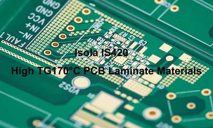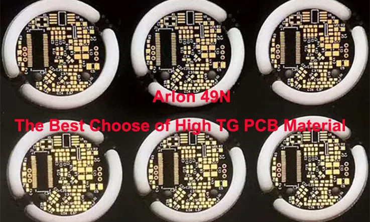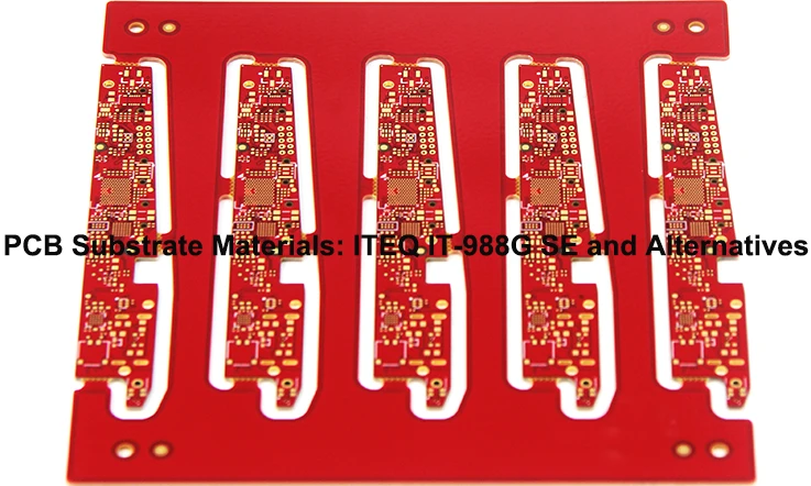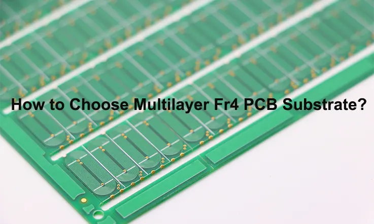
Selecting the appropriate PCB substrate is critical in the realm of electronic design and production. The substrate serves as the foundation for the PCB, furnishing mechanical assistance and electrical shielding for the components and traces on the circuit board. Opting for the right substrate matter can starkly improve the functionality, dependability and manufacturability of the PCB.
This Article we will discuss how to choose multilayer FR4 PCB Substrate, and why it’s so important in the PCB Manufacturing.
Now, Let’s go!
What is FR4?
FR4 is a widely used type of substrate material in the manufacturing of printed circuit boards (PCBs). It is a composite material composed of a woven glass fabric reinforcement impregnated with an epoxy resin binder. The term “FR4” stands for Flame Retardant 4, referring to its fire-resistant properties.
The glass fabric reinforcement provides mechanical strength and stability to the PCB, while the epoxy resin serves as a dielectric material that isolates the conductive traces on the board. FR4’s stellar electrical insulation traits, dimension consistency, and cost efficiency have earned it a wide endorsement in a multitude of applications.
FR4 is available in various grades and thicknesses to meet different performance requirements. It harmonizes with standard PCB manufacturing procedures and can be effortlessly made into multilayer boards, rendering it apt for intricate design requirements. The application of FR4 substrates is widespread, extending to consumer electronics, telecommunication equipment, automotive electronics, industrial control systems, and a broad range of other electronic apparatus and systems.
What’s Mean for Multilayer FR4 PCB Substrates?
Multilayer FR4 PCB substrates refer to printed circuit boards that consist of multiple layers of FR4 material stacked together. In a multilayer PCB, the FR4 layers are separated by thin layers of copper foil, which serve as the conductive pathways for electrical signals.
The construction of a multilayer FR4 PCB involves laminating multiple FR4 layers together using heat and pressure. Each layer is typically etched with copper traces and vias that connect the different layers, allowing for complex interconnections and increased circuit density.
The quantity of strata in a multilayer FR4 PCB can diverge based on circuit complexity and distinctive design requisites. Commonly used layer counts include 4-layer, 6-layer, 8-layer, and higher. The design of multilayer layers superior signal consistency, diminished electromagnetic intrusive effects and a more productive spatial utilization relative to single or double-sided PCBs.
Factors to Consider When Choosing Multilayer FR4 PCB Substrate
When the selection process for a multilayer FR4 PCB substrate is in play, multiple elements demand consideration to guarantee the PCB’s peak performance and dependability. The following are the crucial factors to bear in mind:
1.Layer count:
Ascertain the needed layer account predicated on the intricacy of the circuit andthe desired density of components. A greater count of layers allow for more sophisticated designs and provides an upswing in routing flexibility.
2.Thickness:
Choose the appropriate thickness of the FR4 substrate based on the mechanical and electrical requirements of the PCB. Substrates that are more thick grant enhanced rigidity and can endure higher current levels, whereas thinner substrates yield more compact and flexible results.
3.Dielectric constant (Dk):
Consider the dielectric constant of the FR4 material, as it affects the impedance and signal propagation characteristics of the PCB. Choose a substrate with a consistent and controlled Dk value to maintain signal integrity.
4.Thermal properties:
Evaluate the thermal conductivity and coefficient of thermal expansion (CTE) of the FR4 substrate. These properties impact the PCB’s ability to dissipate heat and withstand thermal stresses. Higher thermal conductivity and a compatible CTE with other components are desirable for efficient thermal management.
5.Flame retardancy:
Ensure that the chosen FR4 substrate meets the required flame retardancy standards for the intended application. FR4 materials are typically flame retardant, but different grades may have varying levels of flame resistance.
6.Surface finish:
Consider the surface finish options available for the multilayer FR4 PCB. Common surface finishes include HASL (Hot Air Solder Leveling), ENIG (Electroless Nickel Immersion Gold), and OSP (Organic Solderability Preservative). The surface finish affects solderability, corrosion resistance, and overall reliability.
7.Manufacturing capabilities:
Verify that the chosen multilayer FR4 PCB substrate is compatible with the manufacturing processes and equipment available. Ensure that the PCB manufacturer has experience and expertise in handling multilayer designs.
8.Cost:
Evaluate the cost-effectiveness of the multilayer FR4 PCB substrate, considering factors such as material cost, manufacturing complexity, and any additional features or requirements.
By considering these factors, you can select a multilayer FR4 PCB substrate that meets the specific needs of your application in terms of performance, reliability, and cost.
How to Select Multilayer Fr4 Substrate Thickness?
Selecting the appropriate multilayer FR4 PCB substrate thickness involves considering several factors related to the specific application and design requirements. Here are some considerations to help you make an informed decision:
1. Mechanical Stipulations: Appraise the mechanical limitations of your application. Take into account constituents such as the allotted space for the PCB, mounting limitations, and any weight constraints. Thicker substrates may provide more mechanical strength and rigidity, which can be beneficial in applications with higher mechanical stress or when components need to be mounted securely.
2. Electrical performance: The thickness of the substrate can influence the electrical performance of the PCB. Usually, Thinner substrates generally offer improved high-frequency performance due to reduced signal propagation delays and lower parasitic capacitance. Conversely, thicker substrates may offer superior control over impedance and fortified power handling capabilities.
3. Thermal Management: Reflect on the heat dissipation needs of your PCB. Thicker substrates can have better heat dissipation capabilities due to increased thermal mass. Therefore, This can be advantageous in applications where heat generation is a concern, as it’s aiding in distributing and dissipating heat in a more proficient manner.
4. Layer count and complexity: The layer count and complexity of your PCB design can influence the substrate thickness selection. Higher layer counts may require thicker substrates to accommodate the additional layers and provide sufficient insulation between them. Complex designs with fine-pitch components or high-density interconnects may benefit from thinner substrates to facilitate precise routing and reduce parasitic capacitance.
5. Manufacturing capabilities: Evaluate the manufacturing capabilities of your PCB manufacturer or supplier. Some manufacturers may have limitations on the minimum or maximum substrate thickness they can handle. Ensure that the selected thickness falls within their manufacturing capabilities to avoid any production issues.
6. Cost considerations: Thicker substrates generally cost more due to the increased material usage. Consider your budget and cost constraints when selecting the substrate thickness. Find a balance between the desired performance and the cost-effectiveness of the chosen thickness.
It’s important to note that there isn’t a one-size-fits-all approach to selecting the substrate thickness. The optimal thickness is largely reliant on your application’s specific demands. It’s advisable to initiate a dialogue with PCB manufacturers, engineers, or industry specialists who can dispense advice, plummeting from their extensive experience and knowledge of similar applications.
Additionally, performing simulations or prototypes can help evaluate the impact of different substrate thicknesses on electrical performance, thermal management, and mechanical stability, allowing you to make an informed decision.
Evaluating Different Multilayer FR4 PCB Substrate Options
When evaluating different multilayer FR4 PCB substrate options, it’s important to consider the following aspects:
Material quality: Assess the quality and reliability of the FR4 material used in the substrate. Look for reputable suppliers and ensure that the material meets industry standards and certifications.
Performance requirements: Determine the specific performance requirements of your PCB, including signal reliability, impedance control, power handling, and thermal management. Selecting for a substrate that efficiently satisfies these stipulations.
Layer count and stackup design: Consider the required layer count based on the complexity of your circuit design. Evaluate the stackup design options offered by different substrate options to ensure they can accommodate your specific needs.
Dielectric properties: Analyze the dielectric attributes of the substrate, comprising the dielectric constant (Dk), dissipation factor (Df), and insulation opposition. These attributes impact signal dissemination, impedance control, and comprehensive circuit performance.
Thermal properties: Evaluate the thermal conductivity, CTE, and glass transition temperature (Tg) of the substrate. These properties determine the substrate’s ability to dissipate heat and withstand thermal stresses, which is crucial for reliable operation.
Flame retardancy: Verify that the substrate meets the required flame retardancy standards for your application. Consider the specific flame retardant rating and any additional certifications or compliance requirements.
Surface finish compatibility: Ensure that the substrate is compatible with the desired surface finish options for your PCB. Different surface finishes offer various advantages in terms of solderability, corrosion resistance, and wire bonding compatibility.
Manufacturing capabilities: Assess the manufacturing capabilities of the PCB suppliers or manufacturers offering the substrate options. Consider their experience, expertise, and equipment capabilities in handling multilayer FR4 PCB production.
Cost-effectiveness: Compare the costs of different substrate options, taking into consideration elements like material cost, fabrication intricacy, along with any supplementary facets or stipulations. Harmonize the expense with the aspired performance and dependability to discover the most fiscally effective option.
By evaluating these aspects you can make an informed decision when selecting the best multilayer FR4 PCB substrate, for your specific use.
How Testing and Validation of Multilayer FR4 PCB Substrate?
Electrical testing:
Electrical testing involves checking the functionality and performance of the PCB by verifying the continuity of the circuitry, measuring impedance, checking signal integrity, and performing functional tests. This appraisal can be facilitated using Automated Test Equipment (ATE) or bespoke testing instruments. Various tests like continuity assessments, impedance verifications, and signal integrity gauging are undertaken to ensure appropriate electrical connectivity and performance.
Thermal testing:
Thermal testing are carried out to scrutinize the thermal traits of the multilayer FR4 PCB substrate. This embraces gauging its talent for heat dissipation, thermal conductivity, and thermal expansion attributes. Thermal imaging, thermal cycling, and thermal resistance measurements are some of the techniques used to assess the thermal performance of the PCB.
Mechanical testing:
Mechanical testing are executed to examine the mechanical robustness, durability, and dependability of the multilayer FR4 PCB substrate. Such tests incorporate trials like bend analyses, flex tests, shake investigations, and impact tests. These tests certify that the PCB can endure mechanical tension, environmental settings, and manipulation throughout its service life.
Environmental testing:
Environmental testing involves subjecting the multilayer FR4 PCB substrate to various environmental conditions to evaluate its performance and reliabilit. This comprises examinations akin to temperature cycling, humidity testing, salt fog analysis, and thermal shock testing. These tests gauge the PCB’s competence to endure temperature shifts, dampness, oxidation, and other environmental elements.
Reliability testing:
Reliability testing is conducted to assess the long-term performance and reliability of the multilayer FR4 PCB substrate. This includes accelerated life testing (ALT), which involves subjecting the PCB to accelerated aging conditions to simulate the effects of prolonged use. ALT helps identify potential failure modes and estimate the lifespan of the PCB.
Signal integrity testing:
Signal integrity testing is performed to evaluate the quality and integrity of the signals transmitted through the multilayer FR4 PCB substrate. This includes tests such as eye diagram analysis, jitter measurements, and impedance measurements. These tests ensure that the PCB can maintain signal integrity and minimize signal degradation or distortion.
Design rule checks (DRC):
DRC involves verifying the PCB design against specific design rules and guidelines to ensure compliance and manufacturability. DRC checks for issues such as trace spacing, pad sizes, solder mask clearances, and other design-related parameters. This helps identify potential design flaws or manufacturing issues that could affect the performance or reliability of the PCB.
It’s important to note that the specific testing and validation methods may vary depending on the application, industry standards, and specific requirements of the multilayer FR4 PCB substrate.
Important of Multilayer FR4 Substrate in Circuit Boards Manufacturung Process
Complex interconnections: Multilayer FR4 PCB substrates allow for the creation of complex interconnections between different components and layers of a circuit board. The multiple layers furnish ample routing space, empowering the construction of sophisticated circuitry and design of high-density interconnects.
Increased circuit density: Multilayer FR4 PCB substrates facilitate the accommodation of additional components and circuitry within confined board dimensions. By piling up numerous layers, the overall circuit density can be significantly increased, allowing for more functionality in a compact form factor.
Better signal integrity: The use of multilayer FR4 PCB substrates helps in achieving better signal integrity by providing controlled impedance routing. The dielectric properties of FR4 material, such as its consistent dielectric constant (Dk), allow for precise impedance control, reducing signal reflections and maintaining signal integrity.
Reduced electromagnetic interference (EMI): The multiple layers in multilayer FR4 PCB substrates act as shielding, reducing the chances of electromagnetic interference. The separation between layers helps contain electromagnetic emissions and provides better isolation between different circuit sections, minimizing EMI-related issues.
Improved reliability: Multilayer FR4 PCB substrates promote elevated dependability courtesy of their sturdy formation. The multilayer layers offer mechanical strength and stability, depreciating the probability of warping or flexing. This contributes to the sustained durability and longevity of the circuit board, predominantly in strenuous surroundings.
Design flexibility: Multilayer FR4 PCB substrates offer design flexibility, allowing for the integration of various circuit components, for instance, power planes, ground planes, and signal layers. This flexibility instigates the creation of complex circuit designs including high-speed digital circuits, RF circuits, as well as mixed-signal circuits.
Manufacturing efficiency: Using Multilayer FR4 PCB substrates makes the manufacturing process more efficient by combining the circuitry into fewer layers. This approach simplifies assembly and testing procedures, minimizes the requirement, for interconnections. Enhances overall manufacturing efficiency.
Cost-effectiveness: Although the preliminary expense of multilayer FR4 PCB substrates may be cost compared to their single-layer or double-layer boards, they present financial benefits in terms of efficient space utilization, simplified wiring intricacy, and enhanced manufacturing productivity. The overall expense per unit of functionality could potentially be lesser when employing multilayer FR4 PCB substrates.
In Conclusion
Choosing the appropriate multilayer FR4 PCB substrate thickness requires considering various factors such as mechanical requirements, electrical performance, heat dissipation, layer count and complexity, manufacturing capabilities, and cost considerations Striking a fine equilibrium between anticipated performance and realistic application restrictions is crucial.
Through an exhaustive evaluation of your application-specific needs, consulting with domain experts, and implementing rigorous testing and validation procedures, you can ascertain an apt selection of a multilayer FR4 PCB substrate thickness, thereby achieving a trustworthy and highly efficient PCB solution.
Our services
Multilayer PCB Manufacturing & Assembly

