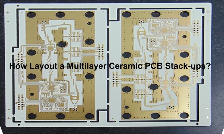
When creating a ceramic PCB stack up it is crucial to take into account multiple aspects like signal integrity, power distribution, thermal management and manufacturability. This piece will explore strategies, for optimizing multilayer ceramic PCB stack ups to guarantee top notch performance and dependability.
Overview of Multilayer Ceramic PCB Stack-ups
A multilayer ceramic PCB stack-up involves the arrangement of multiple ceramic layer and conductive traces in a printed circuit board. These types of PCB are often utilized in applications that require frequencies and temperatures. As their superior electrical and thermal characteristics. Lets take a look, at the components and layers found in a multilayer ceramic PCB stack up:
1. Ceramic Layers: The core of a multilayer ceramic PCB consists of several ceramic layers. Typically it made of materials like alumina or aluminum nitride. These ceramic layer offer thermal conductivity and electrical insulation.
2. Conductive Traces: Thin layers of metal, usually copper, are patterned on the ceramic layers to form conductive paths for electrical signals. These traces are established using method like film or thin film deposition and play a crucial role in connecting the various components and circuits, on the printed circuit board.
3. Vias: Vertical conductive pathways called vias are utilized in PCBs to connect layers facilitating the transmission of signals and maintaining electrical continuity. In the case of multilayer ceramic PCBs these vias are commonly filled with conductive materials such, as tungsten to uphold electrical integrity.
4. Dielectric Layers: Insulation layers, referred to as Dielectric layers are placed between the conductive pathways on various levels to avoid electrical shorts. Typically composed of materials, like glass, alumina or silica these layers boast superior insulation capabilities.
5. Power and Ground Planes: Multilayer ceramic circuit boards commonly contain power and ground planes. These layers serve as pathways to ensure a consistent power source and a stable voltage reference for the circuit. The presence of power and ground planes aids, in minimizing interference enhancing signal reliability and optimizing heat dissipation.
6. Signal Layers: Apart from power and ground planes, multilayer ceramic PCBs may include additional signal layers. These layers contain the traces responsible for carrying the actual signals between components, ensuring proper signal routing and minimizing interference.
7.Solder Mask: A protective layer called solder mask is added to the surfaces of the PCB to shield the conductive pathways from outside elements and avoid any solder connections when putting it together. This layer, usually made of polymer covers the board except, for the spots where soldering needs to take place.
8.Surface Finish: The surface finish serves as a safeguarding layer that is added to the copper pads, on the PCB. It enhances capabilities stops oxidation and boosts the boards reliability. Typical surface finishes used for ceramic PCBs consist of immersion gold, immersion silver and tin lead solder.
Factors to Consider in Designing Multilayer Ceramic PCB Stack-ups
layout the layer stack-up for multilayer ceramic PCB is an essential part of the PCB design process involving thoughtful evaluation of different aspects to guarantee that the board meet performance and reliability standard.
1. Electrical Requirements:
As seen through the eyes of a PCB design engineer it’s vital to plan out the stack up to manage signal trace impedance especially for high speed uses. This helps ensure impedance alignment and reduces signal distortion and crosstalk risks. Also keeping capacitance and inductance between signal traces at a minimum is crucial to maintaining signal quality, in high speed scenarios. Moreover the stack up should deliver power distribution to all parts, especially in high power settings to prevent voltage drops and uphold system stability.
2. Thermal Management:
It’s essential to make sure that the stack up of layer allows heat to escape from the components on the board to keep things running smoothly in high power situations and avoid any harm. Also the layering stack up need to consider how different materials expand when heated to prevent problems. Such as bending or breaking under pressure.
3. Mechanical Constraints:
Ensuring the stack up meets the board thickness standards is vital particularly for applications, with limited space. Moreover the stack up should offer stiffness to endure any vibrations or impacts that the board might face.
4. Signal Integrity:
When creating a stack up it’s important to minimize crosstalk between signal paths in high speed scenarios where crosstalk can lead to signal inaccuracies. Moreover ensuring delay differences between signal paths is vital, in such cases to avoid timing issues.
5. Other Factors:
When considering the stack up design it’s important to think about both the cost and how easy it is to manufacture. Additional layers and using special materials in complex stack ups can raise manufacturing costs significantly. Also ensure that the design matches the manufacturing processes available as intricate stack ups with vias and tight tolerances can pose significant challenges, during production.
Design Guidelines for Multilayer Ceramic PCB Stack-ups
Being a PCB design engineer it’s vital to prioritize the stability and efficiency of the board. A smart approach is to employ a stack up, which helps minimize warping and stress ultimately enhancing the boards overall stability. It’s also important to place power and ground planes to each other to minimize electromagnetic interference (EMI) and enhance power distribution, for improved signal integrity. By including power and ground planes we can further decrease EMI and guarantee smooth operations.
Connecting signal pathways between power and ground layers is a practice to protect the pathways from electromagnetic interference and uphold signal integrity. It is also vital to place vias as near to the components as feasible to reduce inductance. Employing sizes of vias for different functions like using larger ones, for power and ground links and smaller ones for signal paths can greatly improve efficiency. Additionally it is essential to steer of situating vias too closely together to avoid soldering problems and ensure the reliability of the circuit board.
Lastly, employing solder masks and solder paste stencils helps control solder during assembly, preventing solder bridges and other soldering defects.. It’s important to follow the manufacturers recommendations, for materials and procedures to ensure everything work well. Performs at its best. By following these steps you can create a high quality PCB that’s dependable and functions effectively.
Additional Tips:
●Utilize EDA PCB design software with built-in stack-up planning tools to ensure the stack-up meets electrical, thermal, and mechanical requirements.
●Consult with a PCB manufacturer early in the design process for valuable feedback on manufacturability.
●Order prototype boards to validate the stack-up’s performance before initiating full-scale production.
Comparison with Other PCB Stack-up Types
When considering at PCB stack up configurations there are various choices to choose from each having unique features and being suitable, for different uses. Lets compare the multilayer ceramic PCB stack up to other PCB stack up:
1. Multilayer Ceramic PCB:
Material: Multilayer ceramic PCB use ceramic materials, typically alumina (Al2O3) or aluminum nitride (AlN), for their substrate.
Advantages:
●Excellent thermal conductivity and heat dissipation properties.
●High rigidity and dimensional stability.
●Low dielectric loss and excellent high-frequency performance.
●Good resistance to environmental factors such as moisture and chemicals.
Limitations:
●Higher cost compared to other stack-up types.
●Limited availability of large panel sizes.
●Limited flexibility in terms of layer count and design complexity.
2. FR-4 PCB:
Material: FR-4 PCB use a fiberglass-reinforced epoxy laminate as the substrate.
Advantages:
●Widely available and cost-effective.
●Good electrical insulation properties.
●Suitable for a wide range of applications.
●Can support high layer counts and complex designs.
Limitations:
●Lower thermal conductivity compared to ceramic PCBs.
●Limited high-frequency performance.
●More susceptible to moisture absorption and dimensional changes.
3. Flex PCB:
Material: Flex PCB use flexible substrates, typically made of polyimide or polyester.
Advantages:
●Excellent flexibility, allowing for bending and conforming to complex shapes.
●Ideal for applications with space and weight constraints.
●Good resistance to vibration and mechanical stress.
Limitations:
●Limited rigidity and dimensional stability.
●Lower thermal conductivity compared to ceramic or FR-4 PCB.
●Higher cost compared to FR-4 PCB.
4. Metal Core PCB (MCPCB):
Material: MCPCB use a metal core, usually aluminum or copper, as the substrate.
Advantages:
●Excellent heat dissipation properties.
●Suitable for high-power applications.
●Good mechanical strength and rigidity.
Limitations:
●Limited electrical insulation compared to other PCB types.
●Higher cost compared to FR-4 PCB.
●More challenging to manufacture due to the metal core.
The selection of PCB stack up type is based on the needs of the application. Multilayer ceramic PCB is great for frequency and high power applications that require effective thermal management. FR4 PCB provide an option for general purpose applications. Flex PCBs work well for applications needing flexibility whereas MCPCBs are suitable, for high power applications that need heat dissipation.
Advanced Techniques for Optimizing Multilayer Ceramic PCB Stack-ups
Optimizing the stack-up of multilayer ceramic PCB requires utilizing advanced methods that can enhance their efficiency, dependability and ease of manufacturing. Below are some technogies to take into account:
1. Controlled Impedance Design:
●Utilize impedance calculation tools: Use specialized software, or online calculators to determine the required trace width and spacing, and layer stack-up to achieve the desired impedance for high speed signal integrity.
●Differential impedance control: For differential signal pairs, maintain consistent impedance between the traces to minimize skew and crosstalk.
2. Power and Ground Plane Optimization:
●Decoupling capacitor placement: Position decoupling capacitors close to the power and ground pins of the components to minimize inductance and provide effective power distribution.
●Split power planes: Divide the power and ground planes into smaller regions to isolate sensitive circuitry and reduce noise coupling.
●Thermal vias: Strategically place thermal vias near power components to enhance heat dissipation and reduce thermal hotspots.
3. EMI and Signal Integrity:
●Ground stitching vias: Place vias around the perimeter of the PCB to create a solid ground plane and improve EMI shielding.
●Differential pair routing: Route high-speed differential pairs with equal trace lengths, maintaining controlled impedance and minimizing skew.
●Signal layer placement: Separate sensitive analog and high-speed digital signals onto different layers to minimize interference.
4. Thermal Management:
●Thermal vias: Enhance the conduction in regions with high heat dissipation by adding more thermal vias.
●Thermal relief pads: choosing for thermal relief patterns, on power and ground connections to promote improved heat transfer.
●Copper filled vias: Improve conductivity by filling vias with copper.
5. Design for Manufacturability:
●Aspect ratio optimization: Adjust via aspect ratios to optimize manufacturability and reliability, considering the capabilities of the fabrication process.
●Annular ring design: Maintain minimum required annular ring sizes to ensure proper plating and reliability during fabrication.
●Design rule checks (DRC): Perform comprehensive DRC checks to identify and rectify potential manufacturing issues early in the design process.
6. Reliability Enhancement:
●Stress relief cuts: To prevent warping and enhance stability you can create stress relief cuts or grooves in the board.
●Component placement: When placing components take into account their thermal expansion coefficients to reduce the risk of stress related failures.
Sum Up
By adhering to the guidelines and techniques outlined in this article designers can attain peak performance and dependability in multilayer ceramic PCB stack ups. It is crucial to think about signal integrity, power distribution, heat control and manufacturability for effective PCB design. Through layout methods designers can optimize the capabilities of multilayer ceramic PCB stack ups, across different uses.

