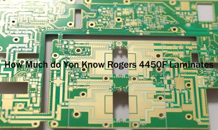
With the expansion of 5G networks, artificial intelligence, and high-speed computing, circuit board materials must keep pace with higher frequencies and tighter signal integrity requirements. MEGTRON-8 PCB Laminate provides a solid foundation for our engineers working on RF, microwave, and high-speed digital applications.
From optimized dielectric constant (Dk) and dissipation factor (Df) for minimal signal loss to high thermal stability and moisture resistance, MEGTRON-8 supports reliable performance in multilayer, HDI, and hybrid PCB designs. Whether it’s reducing EMI, maintaining power integrity, or refining stack-up strategies, this material helps engineers push design capabilities further in next-generation electronics.
This guide explores fabrication techniques, impedance control, thermal management, and design best practices, helping engineers make the most of MEGTRON-8 PCB Laminate in high-speed, high-frequency circuits.
MEGTRON-8 PCB Laminate and Its Industry Demand
With the increasing complexity of high-speed electronic systems, conventional PCB materials are struggling to keep up. Industries that require ultra-reliable, high-performance circuit boards are now leaning toward materials with lower dielectric loss, improved signal integrity, and superior thermal stability.
Let’s explore what MEGTRON-8 PCB Laminate brings to the table and why industries across the board are making the switch.
What is MEGTRON-8 PCB Laminate and How Does It Perform in High-Frequency Applications?
Unlike traditional FR-4 substrates, MEGTRON-8 PCB Laminate is designed for high-speed, high-frequency PCB applications, offering significantly lower signal loss while maintaining excellent processability. This makes it an ideal material for complex multilayer PCBs.
Material Properties and Performance Advantages-
| Property | Impact on High-Speed PCB Performance |
| Low Dielectric Loss (Df) | Enhances signal integrity by reducing transmission loss |
| Stable Dielectric Constant (Dk) | Ensures consistent signal propagation across layers |
| High Thermal Reliability | Withstands extreme temperature variations without degradation |
| Moisture Resistance | Maintains electrical performance in humid environments |
| Process Compatibility | Works seamlessly with advanced PCB manufacturing processes |
With these advantages, MEGTRON-8 PCB Laminate has become a top pick for industries requiring highly reliable signal performance and thermal stability.
Market Demand: Why High-Speed, Low-Loss PCB Materials Are Gaining More Attention?
As technology evolves, faster data rates and lower latency have become non-negotiable. Traditional PCB laminates often introduce unwanted transmission loss, causing performance bottlenecks in 5G base stations, AI processors, and high-speed network devices.
The Rise of High-Speed Data Transmission-
●5G and millimeter-wave (mmWave) technologies require materials with low-loss characteristics to maintain signal quality.
●AI computing and cloud data centers rely on high-speed PCBs to handle massive data transfers without latency issues.
●Aerospace and military communication systems demand high-reliability laminates that function under extreme conditions.
Industries Adopting MEGTRON-8 PCB Laminate: 5G, AI, Aerospace, and More-
Thanks to its high-speed, low-loss characteristics, MEGTRON-8 PCB Laminate is finding its way into multiple high-tech industries.
5G Networks and Telecommunication:
●Used in base stations, RF front-end modules, and mmWave radar systems.
●Low transmission loss preserves signal strength over long distances.
●Multilayer capability supports dense PCB layouts in compact designs.
AI Computing and High-Performance Data Centers:
●Cloud servers depend on low-loss PCBs to maintain high-speed data flow.
●GPUs and AI accelerators need reliable signal pathways for peak efficiency.
●Edge computing devices require robust PCB materials to handle heavy workloads.
Aerospace and Military Applications:
●Radar systems require stable, low-loss laminates for accurate signal processing.
●Satellite communication equipment benefits from moisture-resistant PCBs.
●Avionics and defense electronics need durable, high-temperature-resistant materials.
Why Engineers Are Making the Switch to MEGTRON-8 PCB Laminate?
For PCB designers working on cutting-edge technology, material selection can make or break performance. MEGTRON-8 PCB Laminate offers a combination of reliability, high-speed performance, and process adaptability, making it an attractive option for high-frequency designs.
●Reduces signal loss, making high-frequency designs more effective.
●Improves heat dissipation, ensuring long-term system stability.
●Works well with modern PCB manufacturing techniques.
So, if your project involves 5G communications, AI computing, military-grade electronics, or aerospace systems, now might be the time to reconsider your PCB material choices.
Electrical and Thermal Properties of MEGTRON-8 PCB Laminate
High-performance circuit boards demand materials that maintain signal integrity, withstand extreme temperatures, and offer low transmission loss. In fields like 5G infrastructure, AI-driven computing, and aerospace communications, even a small fluctuation in material properties can affect overall system reliability.
MEGTRON-8 PCB Laminate is designed for these exact challenges. With low dissipation factor (Df), stable dielectric constant (Dk), and excellent thermal endurance, it offers a strong foundation for advanced electronic applications. Let’s explore how its properties meet the needs of next-generation PCB designs.
Low Transmission Loss and High Signal Integrity in MEGTRON-8 PCB Laminate
As frequencies push into the GHz range, signal degradation becomes a major concern. A PCB material with high transmission loss can lead to weakened signals, timing delays, and overall performance drops.
How MEGTRON-8 PCB Laminate Preserves Signal Quality-
●Ultra-low dissipation factor (Df) allows signals to travel with minimal resistance, reducing power loss.
●Consistent impedance properties help maintain clean and accurate data transmission.
●Optimized resin system prevents unwanted distortions, even in complex, high-layer-count boards.
Comparing Transmission Loss Across PCB Laminates-
| PCB Material | Dissipation Factor (Df) @ 1~10 GHz | Best Use Case |
| MEGTRON-8 | 0.0012–0.0016 | 5G, RF, high-speed computing |
| MEGTRON-6 | 0.002-0004 | Telecom, networking |
| Standard FR-4 | 0.015+ | Low-cost applications |
Why Engineers Choose Low-Loss Laminates-
A circuit board running at millimeter-wave frequencies or high-speed digital interfaces needs consistent transmission characteristics. Any deviation can lead to data errors, interference, or excessive heat buildup.
MEGTRON-8 PCB Laminate helps eliminate these risks, ensuring high-frequency signals remain stable throughout the PCB’s lifetime.
Dielectric Constant (Dk) and Dissipation Factor (Df) Optimization for High-Speed PCBs
The right dielectric properties can make or break a high-frequency PCB design. Dielectric constant (Dk) affects impedance matching, while dissipation factor (Df) determines how much energy is lost during transmission.
MEGTRON-8 PCB Laminate’s Dielectric Performance-
| Property | Impact on PCB Behavior | MEGTRON-8 Value |
| Dielectric Constant (Dk) | Controls signal speed and impedance matching | 3.08–3.13 @ 10 GHz |
| Dissipation Factor (Df) | Reduces energy loss and signal distortion | 0.0012–0.0016 |
Why Stable Dielectric Properties Matter-
●Maintains signal timing in high-speed data applications.
●Minimizes phase distortion, which is critical for 5G, radar, and mmWave designs.
●Prevents attenuation, keeping signal strength consistent across long traces.
When our PCB designers demand high-speed, low-loss performance, MEGTRON-8 PCB Laminate provides the electrical stability needed to ensure circuits perform as expected.
Thermal Stability, High Tg, and Moisture Resistance of MEGTRON-8 PCB Laminate
Extreme temperatures, moisture exposure, and repeated thermal cycling can degrade PCB performance over time. MEGTRON-8 PCB Laminate is built to handle these conditions, maintaining its structural and electrical properties even in the harshest environments.
How MEGTRON-8 Handles Heat and Moisture-
| Property | Why It Matters | MEGTRON-8 Value |
| Glass Transition Temperature (Tg) | Prevents softening at high temperatures | 200–220°C |
| Decomposition Temperature (Td) | Withstands lead-free soldering | ≥ 400°C |
| CTE (Coefficient of Thermal Expansion) | Reduces mechanical stress on vias | < 20 ppm/°C |
Durability in Harsh Conditions-
●High Tg prevents layer separation during high-heat processes.
●Moisture-resistant resin system stops electrical drift in humid environments.
●Low CTE ensures stability in multi-layer stackups, even under thermal cycling.
Power Integrity and Thermal Management in MEGTRON-8 PCB Laminate Designs
Handling power fluctuations and heat buildup is a real challenge in high-frequency and high-density PCB designs. MEGTRON-8 PCB Laminate provides a solid foundation for us aiming to improve power stability and heat dissipation in demanding applications.
From minimizing power loss to keeping temperatures in check, selecting the right materials and following well-structured design practices can make all the difference. Let’s break it down.
How MEGTRON-8 PCB Laminate Minimizes Power Loss in High-Density Circuits?
Unstable power delivery can lead to voltage dips, signal disruptions, and poor circuit efficiency. MEGTRON-8, with its low dielectric loss and finely-tuned resin system, allows us to build more efficient and reliable high-speed PCBs.
Reducing Power Plane Noise and DC Drop-
Power integrity issues often arise when circuit density increases, leading to:
●Voltage fluctuations, affecting high-speed components.
●DC resistance buildup, limiting power availability.
●Ground bounce, shifting reference voltages and causing timing issues.
Techniques for Power Optimization-
To get top-tier performance, we typically:
●Use well-placed decoupling capacitors to stabilize voltage rails.
●Optimize power and ground plane stacking for lower impedance.
●Increase copper weight and via density to improve current flow.
By fine-tuning PCB stack-ups and routing, power distribution becomes more efficient, preventing unexpected performance hiccups.
Thermal Conductivity and Heat Dissipation for High-Power Applications
Heat buildup is a silent troublemaker, leading to signal degradation, increased resistance, and shortened component lifespan. MEGTRON-8, with its high glass transition temperature (Tg) and controlled thermal expansion, helps keep things steady even under prolonged stress.
How Heat Affects PCB Performance-
Unchecked thermal rise can cause:
●Dielectric property shifts, altering signal behavior.
●Increased resistance, leading to wasted power.
●Layer delamination, especially in extreme environments.
Strategies for Better Thermal Management-
To keep circuits from turning into mini-heaters, our PCB designers can implement:
●Thermal vias, acting as escape routes for excess heat.
●Wider copper traces, preventing excessive temperature rise.
●Heat spreaders or interface materials, pulling heat away from hot spots.
Many 5G base stations, data center servers, and automotive control units rely on MEGTRON-8 to handle power-hungry applications while maintaining temperature control.
Strategies to Reduce Power Integrity Issues in MEGTRON-8 PCB Laminate Circuits
Even with a solid PCB design, unwanted electrical noise, poor grounding, and inefficient power distribution can create issues. Therefore, we working with MEGTRON-8 fine-tune layouts to prevent power fluctuations and EMI interference.
Common Pitfalls and How to Fix Them-
| Issue | Cause | Solution |
| Voltage ripple | Inadequate decoupling or excessive PDN impedance | Add local capacitors, optimize return paths |
| EMI leakage | Poor isolation between layers | Implement shielding planes and proper spacing |
| Power rail fluctuations | High inductance in traces | Use low-inductance vias and thicker traces |
Enhancing Power Integrity with MEGTRON-8-
By leveraging MEGTRON-8’s low-loss properties, we can:
●Reduce transmission losses, improving efficiency.
●Minimize plane resonance, avoiding interference issues.
●Ensure stable voltage levels, even in high-load conditions.
With proper design tuning, MEGTRON-8 allows power-intensive systems to stay reliable, preventing unwanted voltage swings from throwing performance off track.
MEGTRON-8 PCB Laminate in High-Frequency and RF PCB Applications
The demand for faster data transmission, stable signal processing, and efficient RF performance continues to grow across industries such as 5G networks, aerospace systems, and satellite communications. Achieving clean, interference-free signals requires PCB materials that handle high frequencies while maintaining stability over time.
MEGTRON-8 PCB Laminate is built to handle RF and microwave circuit challenges, offering low transmission loss, predictable dielectric properties, and enhanced thermal endurance. These attributes allow us to develop circuits that perform consistently, even in demanding conditions. The following sections break down how this material contributes to high-frequency PCB designs.
How MEGTRON-8 PCB Laminate Enhances RF and Microwave PCB Performance?
RF and microwave circuits function at frequencies where material consistency directly influences signal behavior. A slight change in dielectric constant (Dk) or dissipation factor (Df) can shift impedance values, resulting in unwanted losses, crosstalk, or performance drops.
Material Properties Supporting RF Applications-
●Low Transmission Loss: Maintains signal strength over longer distances.
●Stable Dielectric Constant (Dk): Supports impedance matching across board layers.
●Low Dissipation Factor (Df): Prevents excessive energy absorption, keeping signals intact.
●High Heat Endurance: Reduces material distortion under extreme conditions.
Comparison of RF Performance in PCB Laminates-
| PCB Material | Dk @ 10 GHz | Df @ 10 GHz | Application Suitability |
| MEGTRON-8 | 3.08~3.13 | 0.0012 | 5G, radar, aerospace RF |
| RO4350B | 3.48± 0.05 | 0.0037 | General RF/microwave |
| FR-4 | 4.2–4.8 | 0.015+ | Standard electronics |
Why Engineers Use MEGTRON-8 for RF Designs-
With lower dielectric loss than conventional laminates and predictable signal behavior, MEGTRON-8 PCB Laminate allows RF engineers to maintain signal clarity across GHz frequencies. This makes it suitable for 5G antenna arrays, millimeter-wave circuits, and military-grade RF designs.
Impedance Control and Insertion Loss Reduction in High-Speed Designs
Keeping impedance within tight tolerances is necessary for stable signal transmission. Uncontrolled impedance variations can lead to signal reflections, timing issues, and reduced efficiency in high-speed networks.
How MEGTRON-8 Maintains Impedance Accuracy-
●Predictable Dielectric Properties: Ensures steady performance across layers.
●Smooth Copper Foil: Reduces conductor loss and enhances signal transmission speeds.
●Advanced Resin System: Supports impedance consistency under environmental changes.
Insertion Loss: The Silent Factor in PCB Performance-
Insertion loss affects how much signal degrades while traveling through a PCB. High-speed networks such as 400G Ethernet, AI processing units, and satellite communication systems rely on low insertion loss to maintain performance.
| Influencing Factor | Effect on Signal Transmission | MEGTRON-8 PCB Laminate Solution |
| Conductor Loss | Higher resistance weakens signals | Smooth copper minimizes resistance |
| Dielectric Loss | Energy is absorbed, reducing signal clarity | Low Df prevents excess absorption |
| Radiation Loss | Stray signals impact efficiency | Consistent Dk avoids unwanted interference |
Keeping Insertion Loss Low for High-Speed Networks-
Applications like 5G telecom infrastructure and radar electronics require steady signal strength across complex circuits. MEGTRON-8 PCB Laminate minimizes insertion loss, preventing performance drops in next-gen technologies.
EMI Shielding and Power Integrity Solutions with MEGTRON-8 PCB Laminate
Electromagnetic interference (EMI) can interfere with RF circuit stability. We working on low-noise amplifiers, high-frequency radar, and satellite communication systems must ensure our PCB materials prevent unwanted signal disturbances.
How MEGTRON-8 Supports EMI Control-
●Low Df prevents reflection-related EMI that affects sensitive signals.
●Impedance consistency avoids stray noise in transmission paths.
●Compatible with shielding techniques, such as copper-filled vias and embedded ground planes.
Power Integrity in High-Frequency Designs-
Stable power delivery is necessary for maintaining signal accuracy in high-frequency PCBs. Voltage fluctuations can introduce timing jitter and performance inconsistencies in RF circuits.
| Power Stability Factor | Effect on Circuit Performance | MEGTRON-8 PCB Laminate Solution |
| Dielectric Absorption | Delays signal processing | Minimizes power loss |
| Thermal Expansion | Alters material properties | Withstands temperature shifts |
| Electrical Consistency | Prevents voltage fluctuations | Supports steady power flow |
Keeping RF and Microwave Circuits Stable-
From satellite receivers to 5G base stations, power fluctuations and EMI noise must be managed to preserve signal quality. MEGTRON-8 PCB Laminate offers us a material option designed for clean, interference-free signal flow.
How to Optimize Signal Integrity for MEGTRON-8 PCB Laminate?
For engineers working with high-speed and high-frequency designs, signal integrity doesn’t just happen by accident. MEGTRON-8 PCB Laminate provides a low-loss dielectric, making it a solid choice for 5G, AI hardware, high-performance computing, and RF applications.
Designing for high-performance signal transmission means applying routing strategies, crosstalk mitigation techniques, and simulation-driven validation. Here’s how to make sure your MEGTRON-8 PCB is engineered for peak performance.
High-Speed Routing Techniques for MEGTRON-8 PCB Laminate Circuits
Routing in high-frequency and GHz-range PCBs comes with its own set of challenges. With MEGTRON-8 PCB Laminate, we must consider transmission line effects, impedance consistency, and signal reflections to ensure data moves as intended.
Controlled Impedance Routing-
Since high-speed signals behave like RF waves, trace dimensions and spacing should be designed with strict impedance matching in mind. Microstrip and stripline structures are widely used for MEGTRON-8 PCB designs, depending on whether traces run on outer or inner layers.
●Microstrip: Used for outer layers, where signal traces reference a single ground plane.
●Stripline: Applied to inner layers, where traces are sandwiched between two ground planes, helping to minimize radiation.
Shorter Trace Lengths, Minimal Stubs-
At high frequencies, even a short stub can act as an antenna, reflecting signals and causing ringing or noise issues. Keeping traces as short and direct as possible reduces loss and distortion in high-speed MEGTRON-8 PCB designs.
Via Optimization for Signal Integrity-
Every via introduces parasitic capacitance and inductance, which can degrade signals. For MEGTRON-8 PCB Laminate, the best approach is to:
●Use back-drilled vias to eliminate unnecessary stubs.
●Opt for blind and buried vias in HDI designs for better performance.
●Ensure via spacing aligns with controlled impedance calculations.
Managing Crosstalk and Reducing EMI in Multilayer MEGTRON-8 PCB Laminate Designs
In dense, high-layer-count PCBs, crosstalk and electromagnetic interference (EMI) can create performance issues if not properly managed. Since MEGTRON-8 PCB Laminate is frequently used in RF, microwave, and ultra-fast computing, keeping interference under control is a core design requirement.
Crosstalk Reduction Through Trace Spacing-
Signals traveling in adjacent traces can interfere with each other, causing data corruption and signal distortion. A common design strategy is the 3W rule, which ensures that traces are spaced at least three times their width apart.
For high-speed differential pairs, maintaining tight coupling (closely spaced traces) prevents external noise from disrupting signal integrity.
Proper Ground Plane Design-
A solid reference plane is necessary for high-speed MEGTRON-8 PCB layouts. Poor ground plane design leads to:
●Ground loops, which introduce noise.
●Uncontrolled return paths, which increase EMI.
●Voltage fluctuations, affecting timing accuracy.
For MEGTRON-8 multilayer stacks:
●Dedicated ground layers help maintain stable return paths.
●Ground stitching vias reduce signal loop area.
●Avoiding split ground planes prevents unwanted current pathways.
Shielding High-Speed Signals from External Noise-
Techniques such as guard traces and copper pour areas help reduce radiated emissions. The low-loss characteristics of MEGTRON-8 PCB Laminate support RF and microwave shielding, though proper layout implementation greatly influences overall performance.
Simulation Tools for Optimizing Signal Integrity in MEGTRON-8 PCB Laminate PCBs
With GHz-range signals traveling through MEGTRON-8 PCB Laminate, simulation-driven design helps ensure a layout works before a single board is fabricated.
Pre-Layout Analysis: Understanding Material Properties-
Before starting a layout, it’s useful to analyze the electrical properties of MEGTRON-8 PCB Laminate using tools such as:
●Polar SI9000 – Models impedance and loss characteristics.
●HyperLynx – Simulates signal integrity and transmission line behavior.
●Ansys HFSS – Evaluates high-frequency electromagnetic performance.
Post-Layout Validation: Catching Problems Before Fabrication-
Once a design is complete, simulation tools can uncover hidden issues like:
●Impedance mismatches, leading to reflections.
●Unexpected crosstalk between adjacent signals.
●Uncontrolled return paths affecting EMI.
Software like Keysight ADS and Cadence Sigrity are frequently used to fine-tune layouts before finalizing Gerber files.
Power Integrity and Signal Timing Optimization-
High-speed PCBs don’t just require strong signal integrity—they also need stable power delivery. Power integrity simulations help optimize decoupling capacitor placement and reduce voltage fluctuations that could disrupt timing.
MEGTRON-8 PCB Laminate vs. Other High-Performance PCB Materials
Human designing next-generation high-speed and RF circuits face an ongoing challenge: selecting a PCB material that balances signal integrity, thermal management, and manufacturability.
Among the contenders, MEGTRON-8 PCB Laminate stands out in applications requiring low loss, controlled impedance, and multilayer integration. But how does it compare with alternatives like MEGTRON-6, Isola, Rogers, and PTFE-based laminates (Teflon)?
Let’s take a closer look at how these materials measure up.
MEGTRON-8 PCB Laminate vs. MEGTRON-6: A Performance Comparison
Panasonic’s MEGTRON series has long been a reliable choice for high-speed PCB manufacturing, but the differences between MEGTRON-6 and MEGTRON-8 make the latter an appealing upgrade for more demanding applications.
Material Property Breakdown-
| Property | MEGTRON-8 | MEGTRON-6 |
| Dielectric Constant (Dk, 10 GHz) | 3.08–3.13 | 3.6–3.8 |
| Dissipation Factor (Df, 10 GHz) | 0.0012–0.0016 | 0.002–0.004 |
| Glass Transition Temperature (Tg) | ~200°C | ~180°C |
| Thermal Conductivity (W/m·K) | Higher | Moderate |
| Moisture Absorption (%) | Lower | Slightly Higher |
Why Designers Are Choosing MEGTRON-8 Over MEGTRON-6-
1.Lower Transmission Loss – MEGTRON-8 allows signals to travel longer distances with less attenuation, making it an excellent fit for high-speed computing and RF applications.
2.Greater Thermal Stability – With a higher Tg and better heat dissipation, it offers stronger reliability under extreme operating conditions.
3.More Predictable Impedance Control – This makes MEGTRON-8 a preferred choice for multilayer PCB stacks, where consistent electrical performance is a must.
For those seeking to enhance signal performance and thermal resilience, MEGTRON-8 provides a straightforward solution compared to its predecessor.
Comparing MEGTRON-8 PCB Laminate with Isola, Rogers, and PTFE-Based Laminates
For applications pushing the limits of high-frequency circuit performance, MEGTRON-8 competes with well-known brands like Isola, Rogers, and PTFE-based laminates (Teflon). Each material has its own trade-offs in terms of signal behavior, processing complexity, and cost efficiency.
Performance Comparison of High-Speed PCB Materials-
| Material | Dielectric Constant (Dk, 10 GHz) | Dissipation Factor (Df, 10 GHz) | Thermal Expansion (Z-axis, ppm/°C) | Processing Requirements |
| MEGTRON-8 | 3.08–3.13 | 0.0012–0.0016 | ~25 | Standard PCB Processes |
| Isola I-Speed | 3.38 | 0.0021 | ~45 | Standard PCB Processes |
| Rogers RO4003C | 3.55 | 0.0027 | ~40 | Requires Special Processing |
| PTFE (Teflon-based) | 2.1–2.5 | 0.0005–0.0012 | ~120 | Challenging to Process |
Key Insights from the Comparison-
1.Rogers laminates are highly effective in RF and microwave designs, but they require special processing techniques like plasma etching. MEGTRON-8 integrates more easily into existing PCB workflows.
2.PTFE-based laminates (Teflon) offer exceptionally low loss, but higher thermal expansion and fabrication complexity make them less suitable for dense, multilayer PCBs.
3.Isola materials work well for general high-speed digital circuits, but they don’t match MEGTRON-8’s balance of low loss and thermal stability.
Selecting MEGTRON-8 PCB Laminate for High-Speed Electronics
The best PCB material choice depends on the frequency range, temperature constraints, and manufacturability of the end product. MEGTRON-8 provides an attractive combination of electrical performance and processing convenience.
Where MEGTRON-8 PCB Laminate Excels-
| Industry | Advantages of Using MEGTRON-8 |
| 5G Infrastructure | Provides low insertion loss across wide frequency bands. |
| Aerospace & Defense | Withstands temperature fluctuations and high-power RF signals. |
| High-Speed Computing | Supports multi-gigabit data transmission with minimal distortion. |
| Automotive Radar | Maintains stable dielectric properties for mmWave radar systems. |
Why Engineers Are Opting for MEGTRON-8-
●Consistent Electrical and Thermal Performance – Unlike PTFE-based laminates, MEGTRON-8 delivers steady signal behavior across a range of frequencies.
●Reliable Manufacturing Process – Rogers and PTFE materials often require non-standard processing steps, adding cost and complexity. MEGTRON-8 integrates into standard fabrication techniques.
●Lower Moisture Absorption – This ensures long-term reliability in humid environments without performance degradation.
Looking to upgrade your high-frequency PCB design? MEGTRON-8 offers a well-balanced solution for demanding applications.
Why Advanced PCB Stack-Up Design with MEGTRON-8 PCB Laminate?
For high-frequency and high-speed electronic designs, choosing the right PCB stack-up ensures reliable signal transmission and stable power delivery. MEGTRON-8 PCB Laminate provides a well-balanced solution with low transmission loss, stable dielectric properties, and strong thermal reliability.
Creating an optimized layer structure requires precise material selection, impedance management, and controlled fabrication methods. Let’s break down how to make the most of MEGTRON-8 in PCB stack-up configurations.
Hybrid PCB Designs: Combining MEGTRON-8 PCB Laminate with Other Materials
We often mix materials in PCB stack-ups to adjust costs, mechanical stability, and electrical properties. MEGTRON-8 PCB Laminate, known for its low dissipation factor and high-frequency stability, is frequently combined with other substrates to fine-tune performance for different circuit layers.
Strategic Material Pairing for Enhanced Performance-
Using MEGTRON-8 in combination with FR-4, polyimide, or PTFE-based laminates allows us to:
●Adjust dielectric properties while maintaining cost efficiency.
●Improve thermal management by selecting materials with a higher glass transition temperature (Tg).
●Enable flex-rigid PCB designs by integrating flexible substrates where needed.
Challenges When Mixing Materials-
Combining materials requires attention to thermal expansion mismatches to prevent delamination. Low-flow prepregs or specialized adhesives help ensure strong bonding between layers.
Applications Benefiting from Hybrid Stack-Ups-
Hybrid designs using MEGTRON-8 appear in:
●5G infrastructure, where high-frequency layers demand low-loss materials, while lower-frequency control layers use cost-effective alternatives.
●Radar and aerospace systems, integrating RF signal layers with mechanical support layers.
●High-performance computing, where signal and power layers need tailored electrical properties.
Controlled Impedance and Layer Stack Optimization for MEGTRON-8 PCB Laminate
High-speed signal transmission depends on layer arrangement, dielectric properties, and trace layout. MEGTRON-8 PCB Laminate, with its low Dk variation and low-loss characteristics, allows for predictable impedance values across the entire PCB.
Fine-Tuning Impedance for High-Speed Signals-
A well-structured PCB stack-up helps maintain stable impedance and minimal signal reflection. Considerations include:
●Copper thickness, affecting impedance calculations and resistance.
●Dielectric spacing, ensuring signal containment.
●Trace width adjustments, optimizing transmission line performance.
Avoiding Signal Distortion in High-Speed Designs-
For circuits carrying 10+ Gbps signals, precise routing strategies prevent:
●Reflections, which distort data transmission.
●Insertion loss, leading to weaker signals over long distances.
●Crosstalk, causing interference between adjacent traces.
By integrating dedicated reference planes, we can improve electromagnetic performance and signal clarity.
Best Practices for Multilayer MEGTRON-8 PCB Laminate Manufacturing
Even with the right design, fabrication challenges can affect PCB quality. Working with MEGTRON-8 PCB Laminate requires adjustments to drilling, lamination, and assembly processes to maintain performance and reliability.
Precision Alignment and Layer Registration-
Since MEGTRON-8 features low thermal expansion, it offers better layer alignment in complex stack-ups. However, precise laser alignment and tooling techniques help prevent:
●Misalignment, affecting impedance and circuit reliability.
●Layer shifting, leading to electrical shorts or open circuits.
●Dielectric inconsistencies, impacting signal performance.
Drilling and Via Structures-
MEGTRON-8 handles laser-drilled microvias well, making it suitable for HDI PCBs. Recommended techniques include:
●Back-drilling, removing unwanted via stubs to reduce signal degradation.
●Tightly controlled aspect ratios, preventing stress on via walls.
●Plasma etching, ensuring clean via surfaces for strong plating adhesion.
Managing Heat and Moisture During Assembly-
Because of its high-temperature stability, MEGTRON-8 withstands multiple reflow cycles. However, pre-baking before soldering minimizes moisture absorption, preventing:
●Delamination, caused by moisture expanding under heat.
●Via reliability issues, leading to weakened connections.
●Electrical inconsistencies, affecting RF and high-speed circuits.
Fabrication and Processing Guidelines for MEGTRON-8 PCB Laminate
MEGTRON-8 PCB Laminate has gained traction among engineers tackling high-frequency and high-speed applications, but achieving its full benefits comes down to how well it’s processed.
From lamination techniques to via structures and etching considerations, fabrication requires strict control over parameters to maintain reliability and performance.
Let’s dive into what works—and what can go wrong—when handling MEGTRON-8 PCB Laminate.
Best Practices for Laminating and Pressing MEGTRON-8 PCB Laminate
Since MEGTRON-8 features a low-loss resin system, managing pressure, temperature, and resin flow during lamination is a major part of ensuring consistent results.
Prepreg selection is the first step. MEGTRON-8’s resin system requires carefully controlled flow to prevent dry spots or excess squeeze-out. When the resin is distributed unevenly, delamination and signal integrity problems become unavoidable.
During pressing, a steady temperature ramp-up prevents stress buildup in the laminate. If the heating rate is too aggressive, trapped moisture or uneven curing can cause defects. A controlled cooling process is just as critical—rapid cooling may lead to dimensional instability that throws off layer alignment.
Lamination pressure also plays a role. Applying too much force over-compresses the dielectric layers, while too little pressure leads to poor bonding between layers. A balanced approach ensures that all layers stay uniform while maintaining the electrical properties that MEGTRON-8 is known for.
Recommended Lamination and Pressing Parameters-
| Lamination Parameter | Recommended Value |
| Prepreg Flow | Moderate – Requires optimized resin distribution |
| Press Temperature | 180–200°C |
| Pressure | 300–400 psi |
| Heating Rate | 2.5–3.5°C per minute |
| Cooling Rate | Controlled to avoid stress buildup |
Key Considerations for a Successful Lamination Process-
1.Prepreg Flow Control – Since MEGTRON-8 uses a specialized resin system, uneven flow can result in delamination or resin starvation. Using the right prepreg stack-up prevents these issues.
2.Pressure and Temperature Management – Applying gradual heat and pressure ensures a uniform bond between layers while avoiding excessive resin squeeze-out.
3.Dimensional Stability – MEGTRON-8 has low Z-axis expansion, which helps prevent warping, but precise layer registration is needed to maintain accuracy in multilayer PCBs.
Via Structures and HDI PCB Manufacturing Considerations
With high-speed and RF circuits becoming more compact, via structures must be designed to handle the demands of next-gen electronics.
Traditional through-hole vias work fine in basic multilayer designs, but for HDI (high-density interconnect) PCBs, microvias and buried vias take center stage. Since MEGTRON-8 is used in RF, 5G, and aerospace applications, via-in-pad designs often come into play.
A major consideration when working with microvias is drilling precision. Since MEGTRON-8 uses a high-performance resin system, laser drilling is recommended over mechanical drilling to avoid cracks and uneven via walls. Once drilled, proper copper plating is necessary to prevent electrical resistance issues and ensure a solid connection across layers.
Types of Via Structures in MEGTRON-8 PCBs-
| Via Type | Use Case | Challenges |
| Through-Hole Via (THV) | Standard multilayer designs | Mechanical drilling precision |
| Blind/Buried Vias | HDI and high-layer-count PCBs | Layer-to-layer alignment |
| Microvias | High-density interconnects | Laser drilling consistency |
| Via-in-Pad (VIPPO) | RF and high-speed circuits | Copper filling and planarity |
How to Optimize Via Structures for MEGTRON-8 PCB Laminate-
1.Drilling Techniques – Laser drilling is a must for microvias to prevent material damage.
2.Plating Considerations – Copper-filled microvias improve thermal and electrical performance.
3.Avoiding Pad Lift-Off – MEGTRON-8 has a robust resin system, but improper drilling and plating can cause pad delamination.
Therefore, for RF and microwave circuits, maintaining consistent impedance is a make-or-break factor. Since vias can act as unwanted signal reflectors, techniques like staggered microvias and back-drilling help reduce signal loss and unwanted crosstalk.
Common Fabrication Challenges and How to Avoid Them
Even with precise manufacturing processes, challenges can arise when working with MEGTRON-8 PCB Laminate.
One of the biggest concerns is resin starvation, which occurs when the prepreg doesn’t distribute evenly across the board. This issue is often the result of incorrect pressure settings during lamination. Ensuring a balanced resin flow and avoiding over-pressing can help sidestep this problem.
Another issue is delamination, often caused by excessive heat during soldering or inadequate pre-baking before lamination. Since MEGTRON-8 has a unique resin formulation, pre-baking the material helps remove moisture and prevent thermal expansion defects.
Copper adhesion is another area where things can go wrong. Over-etching during the fabrication process can lead to weakened copper traces, making them more prone to peeling. Fine-tuning etching parameters and ensuring proper surface preparation before plating can prevent these issues.
Common Issues and Solutions in MEGTRON-8 PCB Laminate Fabrication-
| Challenge | Cause | Solution |
| Resin Starvation | Improper prepreg flow | Use correct lamination pressure and layer stack-up. |
| Delamination | Excessive heat during soldering | Use stepwise heating and proper pre-baking. |
| Copper Peel-Off | Over-etching in high-speed layers | Optimize etching parameters and surface prep. |
| Microvia Cracking | Thermal expansion mismatch | Use staggered vias and reinforced plating. |
Best Practices to Minimize Processing Defects-
1.Pre-Bake the Laminate – Removing moisture before lamination prevents delamination during assembly.
2.Fine-Tune Etching & Plating – Improper etch rates can lead to uneven copper traces, affecting signal performance.
3.Control Drill Parameters – High-speed drilling reduces burr formation and ensures clean via walls.
For high-layer-count PCBs, microvia cracking can become a concern. This typically happens when thermal expansion mismatches put stress on the via structure. To counteract this, using staggered microvia designs and reinforced plating techniques can enhance durability and reduce the likelihood of cracks forming.
MEGTRON-8 PCB Laminate: FAQ
1.Does MEGTRON-8 PCB Laminate require special storage conditions before fabrication?
Yes, MEGTRON-8 PCB Laminate should be stored in a dry, cool environment to prevent moisture absorption, which can affect its performance during fabrication.
2.What are the recommended drill parameters for via formation in MEGTRON-8 PCB Laminate?
Standard drilling parameters can be used, but it’s recommended to use higher precision drills to avoid damaging the laminate, especially for microvia and high-density designs.
3.Can MEGTRON-8 PCB Laminate be used for bendable or flexible PCB applications?
No, MEGTRON-8 is a rigid PCB laminate and is not designed for flexible or bendable applications.
4.How does MEGTRON-8 PCB Laminate compare to ceramic-based substrates in RF designs?
MEGTRON-8 offers excellent performance in RF applications but is typically more cost-effective and easier to work with compared to ceramic-based substrates.
5.Are there any specific plating techniques recommended for vias in MEGTRON-8 PCB Laminate?
Electroplating is commonly used for via plating in MEGTRON-8, but care should be taken to maintain uniform plating, especially for fine-pitch designs.
6.What are the recommended solder mask materials for use with MEGTRON-8 PCB Laminate?
Epoxy-based solder masks, such as those designed for high-frequency PCBs, are recommended for MEGTRON-8 due to their compatibility with the laminate’s properties.