The PCB manufacturing industry is constantly evolving, with various surface finish options available to meet different application requirements. One such surface finish is immersion tin, also known as white tin or stannous tin. Immersion tin has gained popularity due to its cost-effectiveness, excellent solderability, and resistance to tarnish. In this article, we will explore the benefits, challenges, and considerations involved in using immersion tin as a surface finish from the perspective of PCB manufacturers.
What Is PCB Immersion Tin Surface Finish?
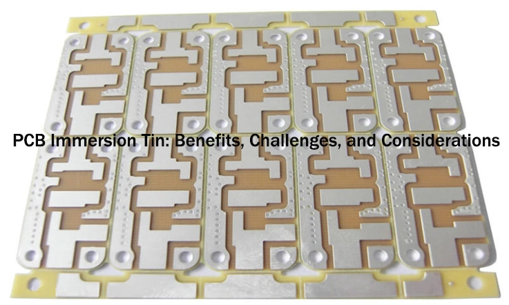
PCB Immersion Tin surface finish, also known as Immersion Tin (ISn), is a metallic coating applied to the surface of a printed circuit board (PCB) to protect it from oxidation, improve solderability, and enhance the overall performance and reliability of the PCB assembly.
The Immersion Tin process involves immersing the PCB in a chemical bath containing a tin-based solution. The tin molecules in the solution bond with the copper surfaces of the PCB through a displacement reaction, forming a thin layer of tin on the copper traces and pads. This tin layer acts as a barrier, preventing the copper from oxidizing and preserving its solderability.
How Immersion Tin on PCB Board Work?
Chemical immersion tin is a widely employed surface treatment process for printed circuit boards (PCBs). Its underlying principle involves altering the chemical potential of copper ions, leading to a chemical substitution reaction with stannous ions in the plating solution. This reaction is electrochemical in nature, resulting in the deposition of reduced tin metal onto the surface of the copper substrate, forming a tin plating layer. The presence of a metal complex adsorbed on the immersion tin plating layer acts as a catalyst for the reduction of tin ions to metallic tin, ensuring a continuous reduction of tin ions.
The chemical immersion tin process serves as an effective PCB copper surface treatment technology. Its products exhibit several advantages over alternative processes. Unlike chemical nickel-gold boards, they do not introduce contamination to the solder. Additionally, no additional polyester layer forms on the solder mask, preserving the original integrity of the PCB. This method enables uniform coverage of a tin layer within any sized PCB hole and connection plate position.
To align with global strategic development and address the increasing demand for lead-free solutions in the PCB market, the adoption of lead-free chemical immersion tin has become a prerequisite for the development plans of companies like DPMC. This shift from the conventional hot air leveling process to tin technology supports the company’s commitment to achieving lead-free manufacturing processes and catering to market demands.
Advantages of Immersion Tin
1. Superior Flatness: Immersion Tin offers excellent flatness, ensuring a high level of precision in PCB assembly.
2. Cost-Effectiveness: Among lead-free finishes, Immersion Tin falls within the mid-range in terms of cost, providing a cost-effective option for various applications.
3. Compatibility with Fine Pitch/BGA/Smaller Components: Immersion Tin is particularly well-suited for fine pitch, Ball Grid Array (BGA), and smaller components, enabling reliable soldering and secure connections.
4. Ideal for Press Fit Technology: When it comes to press fit technology, Immersion Tin is the preferred choice due to its compatibility and ability to facilitate robust press-fit connections.
5. Reworkability: Immersion Tin allows for easy rework, enabling modifications, repairs, or component replacements, thereby enhancing the flexibility and versatility of the PCB assembly process.
Challenges and limitations Use Immersion Tin PCB Surface Finish
Immersion tin (also known as tin plating or white tin) is a popular surface finish used in printed circuit boards (PCBs). While it offers several advantages, it also has certain challenges and limitations that should be considered. Here are some of them:
Shelf Life:
Immersion tin has a limited shelf life compared to other surface finishes like HASL (Hot Air Solder Leveling) or ENIG (Electroless Nickel Immersion Gold). It is sensitive to oxidation, which can reduce its solderability and cause reliability issues if the PCBs are not used within a specific timeframe.
Whisker Growth:
One significant challenge with immersion tin is the potential growth of tin whiskers. Tin whiskers are thin, elongated filaments that can form spontaneously from the tin surface over time. These whiskers can cause short circuits between adjacent conductive traces and lead to reliability problems in high-density PCBs.
Solderability Concerns:
Immersion tin can present challenges with solderability. The tin surface can oxidize quickly, especially when exposed to high temperatures during reflow soldering. This oxidation can affect the wetting properties of the solder, leading to poor solder joint formation and potential solderability issues.
Surface Flatness:
Immersion tin tends to have a relatively rough surface compared to other finishes like ENIG. This roughness can impact the coplanarity of surface-mounted components, potentially leading to difficulties during assembly and soldering processes.
Compatibility with Lead-Free Soldering:
Immersion tin was initially developed for use with traditional tin-lead solder alloys. However, with the shift towards lead-free soldering, compatibility becomes a concern. Immersion tin may not be as compatible with certain lead-free solder alloys, leading to issues such as poor wetting, increased risk of tin whisker growth, or compromised reliability.
PCB Thickness Limitations:
Immersion tin may not be suitable for PCBs with higher thicknesses. The process has limitations in achieving uniform tin thickness on thicker PCBs, which can affect the solderability and overall performance.
Environmental Considerations:
Immersion tin is not considered a RoHS-compliant surface finish due to the presence of tin-lead intermetallic compounds. As a result, it may not be suitable for certain applications that require compliance with environmental regulations.
Aggressiveness towards Soldermask:
Immersion Tin can be aggressive towards soldermask materials, requiring a soldermask dam thickness of more than 5mil to ensure proper protection and prevent damage during the PCB manufacturing process.
Negative Effects of Baking Prior to Use:
Pre-baking Immersion Tin-coated PCBs before utilization can have adverse consequences, impacting the performance and reliability of the finished product. Care should be taken to avoid such practices that may compromise the quality of the PCB assembly.
Immersion Tin Comparison with Other Surface Finishes
When comparing immersion tin with other surface finishes used in PCB manufacturing, two commonly discussed alternatives are Hot Air Solder Leveling (HASL) and Electroless Nickel Immersion Gold (ENIG). Here’s a brief comparison of immersion tin with these two surface finishes:
1. Immersion Tin vs. HASL (Hot Air Solder Leveling):
●Solderability: Both immersion tin and HASL offer good solderability, but immersion tin is often preferred for fine-pitch components and surface mount technology (SMT) applications.
●Flatness: Immersion tin provides a flatter surface finish compared to HASL, which can be advantageous for applications with tight tolerances and precise component placement.
●Shelf Life: Immersion tin has a limited shelf life due to its susceptibility to oxidation, while HASL has a longer shelf life.
●Lead-Free Compatibility: Immersion tin is compatible with both leaded and lead-free soldering processes, making it suitable for environmentally friendly and RoHS-compliant applications.
●Cost: HASL is generally a more cost-effective surface finish compared to immersion tin.
2.Immersion Tin vs. ENIG (Electroless Nickel Immersion Gold):
●Solderability: Both immersion tin and ENIG offer excellent solderability. ENIG is known for its consistent solderability, even after multiple reflow cycles.
●Flatness: ENIG provides a flatter and smoother surface finish compared to immersion tin, which can be beneficial for applications requiring tight control over coplanarity and surface planarity.
●Shelf Life: ENIG has a longer shelf life compared to immersion tin due to the protective gold layer that prevents oxidation.
●Contact Resistance: Immersion tin typically has lower contact resistance compared to ENIG, making it suitable for high-frequency applications.
●Cost: Immersion tin is generally more cost-effective compared to ENIG, which involves a more complex and expensive deposition process.
It’s important to note that the choice of surface finish depends on various factors such as the specific application requirements, assembly processes, environmental considerations, and cost constraints.
How Many Step about PCB Immersion Tin Process?
The immersion tin process is a surface finish technique used in PCB manufacturing. It involves several steps to apply a layer of tin onto the copper traces of the PCB. Here are the key details of the immersion tin process:
1. Cleaning and Preparation: The PCBs undergo a thorough cleaning process to remove any contaminants, dirt, or oxidation from the copper surfaces. This step is crucial to ensure good adhesion and uniform tin deposition.
2. Microetching: After cleaning, the PCBs may undergo a microetching process. Microetching involves applying a mild acid solution to the copper surfaces to remove any oxide layers and promote better adhesion of the tin layer.
3. Flux Application: A flux solution is then applied to the PCBs. The flux helps in promoting wetting and solderability during subsequent processes, such as assembly and soldering.
4. Immersion Tin Bath: The PCBs are immersed in a bath containing a stannous tin solution. The bath typically consists of tin salts, organic additives, and other proprietary chemicals. The PCBs remain in the bath for a specific duration to allow the tin to deposit onto the copper surfaces through a chemical reaction.
5. Rinse and Dry: After the immersion process, the PCBs are rinsed thoroughly to remove any residual chemicals from the tin bath. Deionized water or other suitable rinsing solutions are used. Following rinsing, the PCBs are dried, either through air drying or forced hot air drying, to remove excess moisture.
6. Post-Treatment: In some cases, a post-treatment step may be performed to enhance the performance and reliability of the immersion tin surface finish. This step may involve applying a protective coating or conducting additional surface treatments to improve solderability and prevent oxidation.
It is important to note that the specific details of the immersion tin process can vary among different PCB manufacturers and may be customized based on specific requirements. Process parameters such as bath composition, immersion time, temperature, and rinsing procedures may be adjusted to achieve the desired tin thickness and surface quality.
How Thickness Specifications of Immersion Tin In PCB Fabrication?
The thickness specifications for immersion tin as a surface finish on printed circuit boards (PCBs) can vary depending on industry standards, specific application requirements, and the PCB manufacturer’s capabilities. However, here are some general guidelines for immersion tin thickness:
1. Minimum Tin Thickness: The minimum acceptable thickness for immersion tin is typically around 1 to 2 micrometers (µm) or 40 to 80 microinches (µin). This minimum thickness ensures sufficient coverage and solderability of the underlying copper traces.
2. Nominal Tin Thickness: The nominal or target thickness for immersion tin is often specified between 1.5 to 5 µm or 60 to 200 µin. This range provides a balance between good solderability and cost-effectiveness.
3. Maximum Tin Thickness: There is generally no strict upper limit for immersion tin thickness. However, it is worth noting that excessively thick tin coatings can lead to solderability issues and can negatively impact the coplanarity of surface-mounted components.
The manufacturer’s capabilities, process control, and the desired performance of the PCB in terms of solderability, electrical conductivity, and reliability should all be taken into consideration when determining the appropriate immersion tin thickness for your application.
What is the Shelf life of PCBs Using immersion Tin Surface Finish?
The shelf life of PCBs with immersion tin surface finish can vary depending on several factors, including the quality of the tin finish, storage conditions, and the specific requirements of the application. Generally, immersion tin surface finish has a limited shelf life compared to other surface finishes like immersion gold or HASL (Hot Air Solder Leveling).
Immersion tin is more susceptible to oxidation than other surface finishes, and over time, it may form tin oxide on the surface, which can impact solderability and overall reliability. The shelf life of PCBs with immersion tin finish is typically influenced by the following factors:
1. Storage Conditions: Proper storage conditions play a crucial role in extending the shelf life of PCBs with immersion tin finish. It is important to store the PCBs in a controlled environment with low humidity and temperature. Exposure to moisture, high humidity, or extreme temperature variations can accelerate the oxidation process and reduce the shelf life of the tin finish.
2. Protective Measures: To enhance the shelf life of immersion tin PCBs, manufacturers may apply protective coatings or packaging materials that provide a barrier against moisture and oxidation. These protective measures can help to slow down the oxidation process and extend the shelf life of the PCBs.
3. Application Requirements: The intended application of the PCBs also affects their shelf life. If the application demands long-term reliability or exposure to harsh environments, the shelf life of immersion tin PCBs may be shorter compared to applications with less stringent requirements.
Conclusion
As PCB manufacturers strive to meet the demands of diverse industries, choosing the right surface finish is crucial. Immersion tin provides an attractive option with its cost-effectiveness, excellent solderability, and resistance to tarnish. However, it also comes with challenges and limitations, such as shelf life, solderability concerns, and the potential growth of tin whiskers. PCB manufacturers must carefully evaluate the specific requirements of their customers’ applications and consider factors like shelf life, compatibility with lead-free soldering, and environmental considerations.
By understanding the benefits and limitations of immersion tin surface finish, PCB manufacturers can make informed decisions about incorporating this surface finish into their production processes. Additionally, regular communication and collaboration with customers and surface finish suppliers can help ensure that the immersion tin surface finish meets the desired performance and reliability standards. Ultimately, by leveraging immersion tin and other surface finishes effectively, PCB manufacturers can contribute to the production of high-quality PCBs that meet the needs of a wide range of applications.

