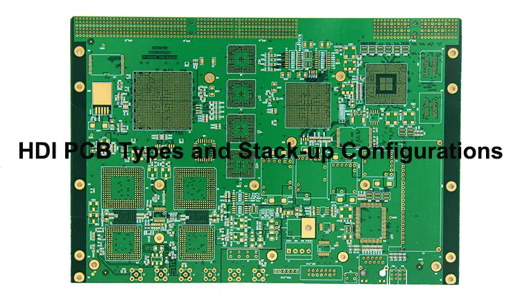
HDI PCB have revolutionized the electronics industry by enabling miniaturization and increased functionality in electronic devices. These sophisticated PCBs provide elevated interconnect density, superior signal integrity and augmented reliability. A pivotal element in HDI PCB design is the stack-up configuration, which dictates the arrangement and composition of the different layers within the PCB. This article aims to examine the diverse categories of HDI PCB and investigate the critical considerations inherent in their stack up design.
Importance of Stack up in HDI PCB
The stack-up configuration holds critical significance in the design and manufacture of HDI PCB. It pertains to the arrangement and composition of distinct layers within the PCB, encompassing signal, power, and ground planes. This configuration directly impacts the HDI PCB’s electrical performance, signal integrity, power distribution and manufacturability. Below are pivotal reasons underscoring the importance of stack-up in HDI PCB design:
1. Signal Integrity: The stack-up configuration is critical in maintaining optimal signal integrity. Through precise engineering of the layer stack up, designers are able to control impedance, reduce crosstalk and mitigate signal distortion effectively. The proper arrangement of signal and ground planes in the stack-up helps in achieving controlled impedance controlled impedance, an essential factor for high speed data transmission and preserving signal integrity.
2. Power Distribution: HDI PCB often incorporate advanced and complex electronic components that require stable and efficient power distribution. The stack-up configuration facilitates the designation of specific power and ground planes, which enhances power delivery while mitigating noise and interference. The tactical positioning of these power and ground planes is crucial in minimizing voltage drop and ensuring an adequate power supply to all components.
3. EMI/EMC Considerations: With the increasing complexity and density of electronic devices, electromagnetic interference (EMI) and electromagnetic compatibility (EMC) have become critical concerns. The stack-up design can include dedicated ground planes and shielding layers to mitigate EMI/EMC issues. Proper isolation and shielding can help reduce the coupling of electromagnetic radiation and improve the overall performance and reliability of the HDI PCB.
4. Thermal Management: HDI PCB frequently emit considerable heat, a consequence of their compact architecture and high-density components. The stack up configuration can incorporate thermal management technology, including thermal vias, thermal planes and heat sinks, to efficiently dissipate heat and maintain ideal operational temperatures. Efficient thermal management is crucial for ensuring the reliability and lifespan of electronic components.
5. Manufacturing Considerations: The stack-up design must also consider manufacturing constraints and requirements. This involves consider the capabilities and limitations of the fabrication processes employed in HDI PCB production, including sequential lamination, laser drilling, and plating processes. A meticulously optimized stack-up design facilitates manufacturability, streamlines assembly, and promotes cost efficiency.
Therefore, the stack-up configuration plays a pivotal role in realizing superior electrical performance, signal integrity, power distribution, EMI/EMC adherence, thermal management, and manufacturability in HDI PCB. A meticulously crafted stack-up is instrumental in the seamless incorporation of intricate circuit designs, bolsters the PCB’s reliability, and guarantees the proficient functioning of contemporary electronic apparatus.
Types of HDI PCB
In the realm of HDI PCB, several distinct types exist, each characterized by unique features and applications.
Microvias: Microvias, with diameters below 150 microns, are crafted using laser drilling or mechanical drilling techniques. They facilitate high density interconnections and signal routing within the PCB.
Blind Vias: Unlike through hole vias, blind vias do not traverse the entire thickness of the PCB. They establish connections between different layers without being exposed on the surface. These vias are used to accommodate buried components and enable efficient signal routing.
Buried Vias: Buried vias remain concealed within the inner layers of the PCB and are not present on any surface. Their primary purpose is to facilitate high density interconnections and signal routing within intricate multi layer PCB.
Sequential Lamination:This fabrication process involves the lamination of multiple layers of copper foil and prepreg, resulting in sophisticated multi-layer structures with a high density of interconnects. Sequential lamination is particularly applicable in high performance domains such as telecommunications and data processing.
Build-Up: The build-up process involves incrementally constructing the PCB layer by layer, enabling the incorporation of blind and buried vias. This allows for high density interconnections and signal routing within complex multi layer structures.
Common Stack up Configurations for HDI PCB
There are several common stack up configurations used in HDI PCB, depending on the specific design requirements and manufacturing capabilities.
4 Layer Stack up:
●Top Layer: Signal traces and components
●Layer 2: Ground plane
●Layer 3: Power plane
●Bottom Layer: Signal traces and components
This stack-up configuration is suitable for simple HDI PCB designs with moderate complexity and lower layer count.
6 Layer Stack up:
Top Layer: Signal traces and components
Layer 2: Ground plane
Layer 3: Signal traces and components
Layer 4: Ground plane
Layer 5: Power plane
Bottom Layer: Signal traces and components
This 6 layer stack up offers enhanced flexibility for routing high speed signals while separating power and ground planes to improve signal integrity.
8 Layer Stack up:
●Top Layer: Accommodates signal traces alongside components
●Layer 2: ground plane
●Layer 3: Houses signal traces in addition to components
●Layer 4: ground plane
●Layer 5: Designed to hold signal traces and necessary components
●Layer 6: ground plane
●Layer 7: Dedicated entirely as power plane
●Bottom Layer: Consists of signal traces along with components
This 8 layer configuration provides a superior level of routing agility and accommodates higher complexity in design, enabling higher density. Furthermore, it enhances signal integrity through its detailed engineering approach.
10 Layer Stack Up:
Top Layer: Comprises signal traces and components
Layer 2: Acts as round plane
Layer 3: Accommodates additional signal traces and components
Layer 4: Another ground plane
Layer 5: Houses more signal traces and components
Layer 6: As ground plane
Layer 7: Signal traces and components
Layer 8: Acts as ground plane
Layer 9: Serves as power plane
Bottom Layer: The final layer contains signal traces and components
The 10 layer stack up is suitable for highly complex HDI PCB with stringent signal integrity requirements and high density interconnections.
Factors to Consider in HDI PCB Stack up
When designing and fabricating HDI PCB, meticulous attention should be paid to the stack up configuration, which encompasses the arrangement and composition of the various layers within the PCB. Several key factors must be carefully considered:
Material Selection:
Careful consideration should be given to the selection of appropriate core materials, such as FR4, polyimide, or metal-backed substrates, which provide structural support to the PCB. The choice of prepreg, a resin-coated copper foil used to bond the layers, also significantly impacts the electrical and thermal properties of the PCB.
Layer Count and Thickness:
Determining the number of layers in an HDI PCB is contingent upon the design’s complexity. While additional layers facilitate higher interconnect density, they also escalate costs and fabrication complexity. The thickness of each layer should be specified based on the required signal integrity and power handling capabilities.
Aperture Size and Vias:
The aperture size, referring to the diameter of vias, is a critical consideration. Smaller vias allow for higher interconnect density but can present challenges and elevate fabrication costs. The type of vias employed, such as microvias, blind vias and buried vias, depends on the design requirements and manufacturing capabilities.
Interconnect Technology:
Selecting the appropriate interconnect technology is essential for effectively connecting the layers of the PCB. Options include plated through holes, microvias, and controlled impedance traces. The choice of interconnect technology greatly affects the electrical performance and overall reliability of the PCB.
Impedance Control:
Maintaining impedance control is imperative for high speed digital applications. The stack up design must ensure that the desired impedance is consistently maintained throughout the signal path. This entails meticulous management of trace width, spacing, and the selection of suitable dielectric materials.
How to Layout the HDI PCB Stack Up Step by Step?
Here is a step by step guide to laying out HDI PCB stack up:
1. Define the Design Requirements:
Begin by clearly defining the design requirements, which encompass the number of layers, desired signal speeds, and any special considerations such as impedance control or high power handling capabilities.
2. Choose the Core and Prepreg Materials:
Select the appropriate core materials, including options such as FR4, polyimide, or metal backed substrates, aligning them with the design requirements and the capabilities of the fabrication process. Similarly, choose the prepreg materials that best meet the electrical and thermal properties necessary for the PCB.
3. Determine the Layer Stack up:
In alignment with the design specifications, ascertain the requisite quantity of signal, power, and ground layers. Arrange the layers in a logical order to optimize signal routing and minimize crosstalk. For improved signal integrity, it’s advisable to position high speed signal layers in proximity to ground planes.
4. Define the Via Types and Locations:
Determine the precise varieties of vias necessitated by the design, including microvias, blind vias and buried vias. Implement a strategic deployment of these vias to mitigate signal attenuation and maintain impedance control. Consider symmetry and equilibrium in the placement of vias to enhance signal integrity.
5. Design the Signal Traces:
Route the signal traces on the appropriate layers while considering signal integrity and crosstalk. Utilize controlled impedance traces when necessary for high speed signals. Adhere to optimal trace spacing guidelines to reduce crosstalk and maintain precise impedance control.
6. Add Power and Ground Planes:
Integrate power and ground planes to furnish a robust voltage reference point and diminish electrical noise. Connect the power and ground planes to the appropriate vias and traces, ensuring sufficient capacitance for power distribution and effective return paths for signal currents.
7. Optimize the Stack up for Impedance Control:
Calculate the characteristic impedance of the signal traces based on the stack up geometry, trace width, spacing and dielectric materials. Adjust these parameters as needed to achieve the desired impedance control. Utilize simulation tools or impedance calculators for accurate calculations.
8. Review and Verify the Stack up:
Conduct a comprehensive examination of the stack up to confirm its compliance with all design specifications, considering factors such as signal integrity, power distribution, and impedance regulation. Employ simulation tools or engage with specialists to validate signal functionality and impedance adherence.
9. Finalize the Stack up and Generate Fabrication Files:
Upon finalization and verification of the stack up, it is imperative to produce the requisite fabrication documents, including Gerber files, for the manufacturing process. It is crucial to ensure that all layers, vias, and traces are precisely delineated in these fabrication files.
Additional Tips:
●Utilize design software with HDI specific capabilities to simplify the stack up design process.
●Seek guidance from a reliable PCB fabrication house to understand achievable stack up and any specific fabrication limitations.
●Leverage impedance calculators and simulation tools to optimize the stack up for signal integrity and impedance control.
●Maintain sufficient spacing between signal traces and vias to minimize crosstalk and maintain impedance control.
In a Word
HDI PCB provide significant benefits in miniaturization, signal integrity and high density interconnectivity. By choosing the correct HDI PCB types and customizing the stack-up to address specific design criteria, engineers can develop high performance, reliable and cost efficient PCB solutions.
Regardless of whether the design calls for 4 layer, 6 layer, 8 layer, or 10 layer stack up, meticulous selection of materials, via types and placements, impedance control and effective power distribution are paramount. Engaging in collaboration with seasoned PCB manufacturers like JarnisTech and leveraging sophisticated design software further contributes to the success of HDI PCB projects. As HDI technology continues to evolve, it paves the way for enhanced prospects in miniaturization and high-density integration within the PCB design arena.

