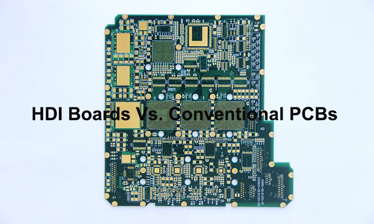
HDI board, known as High Density Interconnect boards have transformed the world of printed circuit boards by presenting an advanced option compared to conventional PCB. These advanced PCB offer a range of benefits making them ideal for applications that demand efficiency space saving design and improved performance. This conversation explores the distinctions, between HDI boards and standard PCB shedding light on their distinct characteristics, advantages and possible applications.
Definition of High Density Interconnect Boards
High Density Interconnect boards represent a specialized types of printed circuit boards that exhibit a remarkable concentration of electrical interconnections within a compact form factor. These boards offer distinctive features and advantages, including:
High Layer Count: HDI boards typically possess 8 or more layers, with certain designs incorporating 30 layers or even higher. This multi layer configuration enables efficient signal routing and accommodates a greater number of components.
Fine Lines and Spaces: HDI boards are characterized by their slender traces and spacing, typically gauging 50 microns or below. This precision-line feature enhances routing density and enables the incorporation of intricate circuitry within a confined space.
Micro-Vias: HDI boards incorporate micro-vias, defined as vias with diameters not exceeding 100 microns, to forge links between disparate layers. These diminutive diameter vias augment interconnect density, facilitate high-density routing, and contribute to miniaturization efforts.
Advanced Materials: HDI boards customarily utilize high-grade materials for their substrates and conductors. Polyimide, a substrate material renowned for its exemplary electrical attributes, temperature resistance and dimensional steadiness, is frequently employed. Copper, recognized for its exceptional conductivity, is typically the conductor material of choice.
HDI boards have gained significant prominence in modern electronics, catering to the demands of various applications that necessitate smaller form factors, heightened performance and expanded functionality.
Construction Differences Between HDI and Conventional PCB
When contrasting HDI boards with conventional PCB, numerous construction variances become evident. These disparities are fundamental in facilitating the superior capabilities of HDI boards. Here are the salient differentiators:
Layer Count and Stack Up:
HDI boards are characterized by a more substantial layer count, typically spanning from 8 to 20 layers or beyond, in contrast to conventional PCB. The stack-up architecture of HDI boards is more complex, featuring interlaced layers of signal, power and ground planes.
Interconnect Density and Pitch:
HDI boards demonstrate a markedly higher interconnect density compared to conventional PCB. The pitch, denoting the spacing between traces, can diminish to 50 microns or less in HDI boards. This decrease in pitch facilitates an increased number of routing channels within a specified area.
Fine Line and MicroVias:
HDI boards utilize fine-line traces with widths not exceeding 50 microns, allowing for the integration of a higher number of traces within constrained spaces. Furthermore, micro-vias, characterized by diameters of 100 microns or below, are employed for inter-layer connections, thereby minimizing the dependency on through-hole vias that are prevalent in conventional PCB designs.
Buried and Blind Vias:
HDI boards often make use of buried and blind vias, which connect internal layers without being exposed on the outer surface of the board. The implementation of these vias enhances signal integrity, reduces the risk of solder bridging, and contributes to overall design efficiency.
Substrate Materials:
HDI boards frequently utilize polyimide or alternative high performance substrates, in contrast to the conventional FR4 material prevalent in standard PCB. These polyimide substrates provide superior electrical characteristics, elevated temperature resilience, and improved dimensional stability, aligning them closely with the demands of HDI technology.
Surface Finishes:
HDI boards frequently incorporate gold or nickel plating as the surface finish. These finishes enhance solderability and protect against oxidation. Among the commonly employed surface finishes for HDI boards is electroless nickel immersion gold (ENIG).
Fabrication Techniques:
The fabrication process for HDI boards involves specialized equipment and techniques. Laser drilling is employed to create micro-vias with precise dimensions, while high precision imaging is used for fine line trace formation. The manufacturing process for HDI boards demands meticulous quality control and adherence to stringent standards.
Material and Process Considerations for HDI Board
The choosing of materials, coupled with the precise of fabrication procedures, hold a significant impact on the performance and dependability of HDI boards. It’s imperative to factor in several crucial aspects to ensure optimal results.
Substrate Materials:
When it comes to HDI board, the commonly used FR4 material, which is prevalent in conventional PCB, may not be suitable due to its comparatively lower thermal stability and higher moisture absorption. On the other hand, polyimide emerges as a superior material, boasting exceptional electrical characteristics, robust temperature resistance and minimal moisture retention. As a result, polyimide often serves as the substrate material in HDI board. Moreover, for specialized application, sophisticated materials such as hydrocarbon resins and ceramic substrates might be incorporated.
Copper Foils:
While conventional PCB commonly employ standard copper, its increased resistivity and heightened likelihood of electromigration might restrict its applicability for HDI board—especially those necessitating high speed signal transmission and power provision. In contrast, high conductivity copper, characterized by lower resistivity and a greater ability to accommodate high current loads, becomes a suitable selection for such HDI board. Furthermore, to reduce signal loss and boost impedance control, HDI board utilize copper foils of a thinner scale, specifically 18 microns or less.
Micro-Via Fabrication:
The production of micro-vias is an integral component of HDI board manufacturing. Laser drilling proves to be a precise and efficient technique for generating micro-vias with high aspect ratios, thereby guaranteeing maximum performance. Although plated-through holes can be utilized for micro-via formation, this process tends to be slower and less precise compared to laser drilling.
Surface Finishes:
The application of surface finishes is vital in guaranteeing the performance and durability of HDI board. Gold plating is a frequently adopted surface finish, prized for its superior solderability and resistance to corrosion. In contrast, nickel plating could be considered as a viable alternative, delivering similar solderability with enhanced wear resistance. Electroless nickel immersion gold (ENIG), a widely favored surface finish option, amalgamates the advantages of both nickel and gold plating to offer outstanding solderability and corrosion resistance.
Process Control:
Rigorous process management is the cornerstone of realizing the targeted quality and dependability of HDI boards. Cutting edge manufacturing equipment and exacting process parameters are indispensable in creating the fine lines, micro-vias, and intricate stack ups that are distinctive of HDI boards. By exercising stringent control over these processes, manufacturers can satisfy the rigorous requirements of high-performance electronic gadgets.
Electrical Performance of HDI Boards
HDI boards display enhanced electrical performance relative to conventional PCB, a testament to their advanced design and composition.
Impedance Control:
HDI boards excel in precise impedance control, facilitated by their fine lines and controlled stack-up. This meticulous control ensures optimal signal integrity and minimizes reflections, making it particularly critical for high-speed digital signals and high-frequency analog circuits.
Signal Integrity:
HDI board are engineered to reduce signal loss and crosstalk, leading to an enhancement in signal integrity. This accomplishment is actualized through the employment of superior quality material, strict adherence to manufacturing tolerances, and the use of progressive design methodologies.
High Speed Signal Routing:
The low signal loss and controlled impedance characteristics of HDI boards make them well-suited for routing high speed signals. They can efficiently uphold data rates reaching 40 Gbps and even exceeding this, catering to the requirements of contemporary high-speed communication protocols.
Crosstalk Reduction:
The dense interconnect structure and controlled routing inherent to HDI boards aid in diminishing crosstalk between neighboring signals. This decrease in undesired signal interference is vital for preserving signal quality and averting errors, especially in high density circuits.
Electromagnetic Interference (EMI) Reduction:
HDI boards utilize high grade materials and progressive design methods to lessen electromagnetic interference. Through meticulous management of signal paths and the application of shielding tactics, HDI boards assist in curtailing EMI effects that could potentially interfere with the functioning of delicate electronic components.
Power Delivery:
HDI boards are designed to efficiently manage high power densities. They feature a robust power distribution network that incorporates multiple power planes and vias. This design strategy guarantees low impedance routes for current flow, facilitating efficient and dependable power delivery.
Manufacturing Challenges and Costs of HDI Board
The sophisticated design and assembly of HDI board introduce numerous production challenges and cost considerations that must be accounted for.
Specialized Equipment and Processes:
The fabrication of HDI boards demands the utilization of specialized equipment and processes, including laser drilling devices, high accuracy imaging systems and advanced plating technology. These specialized equipment may be expensive to procure and necessitate professional operators for effective operation.
Complex Fabrication:
The complexity in HDI board designs, characterized by fine lines, micro-vias and sophisticated layer stack up, renders the fabrication process more complex and time intensive. It demands strict adherence to quality control measures to ensure the desired reliability and performance of the board.
Material Costs:
HDI board utilize high performance substrate such as polyimide and high conductivity copper, which generally carry a higher price compared to the materials employed in conventional PCB. The choice of these materials contributes to the elevated cost of HDI board manufacturing.
Yield:
The production of HDI board demands the application of specialized testing and inspection techniques to ensure their electrical performance and reliability. The inclusion of these extra stages in the manufacturing workflow adds to the total cost.
Test and Inspection:
HDI boards require the implementation of specialized testing and inspection methodologies to ascertain their electrical functionality and dependability. These additional steps in the manufacturing process contribute to the overall cost.
Volume Production:
Establishing a production line for HDI board incurs substantial cost, making it less cost effective for low volume production. The economies of scale associated with higher production volumes can help offset these initial expenses.
Cost Considerations:
The price of an HDI board can fluctuate depending on various elements, such as the board’s dimensions and intricacy, the quantity of layers, choice of materials, surface finish and production quantity. Generally, HDI boards are typically pricier than standard PCB due to the manufacturing challenges and expenses encountered. However, their exceptional performance and compact size frequently validate the elevated cost in many uses.
Importance of HDI Technology in Modern Electronics
HDI technology has surfaced as an essential element in contemporary electronics, propelled by the escalating requirement for compact, lightweight and more potent devices. The significance of HDI technology is rooted in its capability to cater to the changing requisites of diverse applications and unveil a multitude of advantages.
Miniaturization: High density interconnect boards help to incorporate components in a limited space supporting the downsizing of electronic devices. This is particularly vital for gadgets, like smartphones tablets and wearables where size and weight play a significant role.
Enhanced Performance: HDI boards provide high speed signal routing and precise impedance control, which are indispensable for attaining peak performance in applications like data centers, networking hardware and automotive electronics. The technology guarantees trustworthy and efficient data transmission, reducing signal loss and latency.
Increased Functionality: HDI boards are proficient in integrating an extensive array of components, encompassing both passive elements (resistors, capacitors, inductors) and active constituents (IC, transistors). This integration facilitates superior functionality and curbs the dependency on external component, resulting in more condensed and streamlined designs.
Improved Reliability: HDI boards employ advanced materials and manufacturing processes, such as polyimide substrates and laser-drilled micro-vias. These innovations result in enhanced reliability, durability, and longer lifespan for electronic devices. The use of high-quality materials and precise manufacturing techniques ensures better resistance to environmental factors and mechanical stress.
Power Efficiency: HDI technology optimizes signal routing and curtails parasitic impacts, leading to reduced power usage. This is especially vital for battery driven devices, as it aids in extending battery longevity and enhancing energy efficacy.
The importance of HDI technology is evident in various applications where space constraints, performance demands and reliability are critical factors. Some notable examples include:
●High Performance Computing: HDI boards play a vital role in HPC systems by enabling high data rates, low latency and efficient signal transmission, thereby enhancing overall system performance.
●Mobile Devices: HDI boards enable the integration of multiple functions into compact smartphones, tablets, and wearable, enabling manufacturers to deliver powerful and feature-rich devices while maintaining a slim form factor.
●Automotive Electronics: HDI boards find extensive use in automotive applications, including advanced driver assistance systems (ADAS), infotainment systems, and powertrain control modules. The technology supports the increasing complexity and connectivity requirements of modern vehicles.
●Medical Devices: HDI technology finds its application in medical apparatus like implantable devices, diagnostic device and surgical automatons. The compact dimensions, dependability, and superior performance traits of HDI boards render them apt for crucial medical applications.
Final Thoughts
HDI boards and conventional PCB signify two separate methodologies in the realm of electronic interconnectivity. Traditional PCB are apt for uncomplicated designs and cost aware applications, whereas HDI boards thrive in offering superior density, dependability, and performance for present-day electronic systems. The progressive structure, precise fabrication processes, and augmented electrical features of HDI boards render them progressively crucial in fields such as telecommunications, automotive, aerospace, and consumer electronics.
As technological advancement persists, the need for compact, speedier, and more potent electronic devices remains constant. HDI boards, with their capacity to fulfill the stringent requirements of these applications, will persistently hold a central role in empowering the forthcoming generation of inventive electronic products. By grasping the critical differences between HDI boards and traditional PCB, designers and manufacturers can execute informed decisions to exploit the advantages of HDI technology and drive the evolution of advanced electronic systems.

