In the ever-evolving field of PCB manufacturing, engineers are constantly seeking the most reliable and durable surface finishes for their designs. One such surface finish that has gained popularity is the PCB plating hard gold surface finish. Hard gold surface finish offers exceptional benefits, including enhanced durability, corrosion resistance, and excellent electrical conductivity.
This article aims to explore the advantages and considerations of using hard gold surface finish in PCB manufacturing, providing valuable insights for engineers looking to optimize their designs.
What is Hard Gold Surface Finish on PCBs?
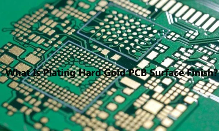
Hard gold surface finish, also known as Hard Electrolytic Gold, is a type of surface finish used on printed circuit boards (PCBs) to provide corrosion resistance, durability, and electrical conductivity. It is a layer of gold that is plated onto the exposed copper pads and traces of a PCB.
Hard gold surface finish is characterized by its thickness and hardness compared to other surface finishes like soft gold or immersion gold. It typically has a gold thickness ranging from 30 to 50 microinches (0.75 to 1.25 microns). The hardness of hard gold surface finish is achieved by adding a small amount of cobalt or nickel to the gold plating solution during the electroplating process.
Performance Characteristics of Hard Gold Surface Finish
Hard gold surface finish offers several performance characteristics that make it a desirable choice for certain applications on printed circuit boards (PCBs). Here are some key performance characteristics of hard gold surface finish:
1.Durability:
Hard gold plating provides excellent durability and wear resistance due to the addition of cobalt or nickel during the plating process. This makes it highly resistant to repeated physical contact, such as when connectors are mated and unmated frequently. The hard gold layer maintains its integrity and does not wear easily, ensuring long-lasting functionality and reliability.
2.Corrosion Resistance:
Gold is inherently resistant to corrosion, and the thicker gold layer in hard gold plating enhances this resistance further. It provides a protective barrier against moisture, oxidation, and other environmental factors that can cause corrosion on the PCB surface. This corrosion resistance ensures the reliability and longevity of the PCB, especially in harsh or corrosive environments.
3.Electrical Conductivity:
Gold is an excellent conductor of electricity, and hard gold plating maintains this conductivity. It ensures low contact resistance and reliable electrical performance in applications where electrical signals need to be transmitted accurately and efficiently. The low contact resistance also prevents signal loss or degradation, making hard gold surface finish suitable for high-frequency and high-speed applications.
4.Solderability:
Although hard gold plating is relatively hard, it still offers good solderability. The gold layer provides a reliable solderable surface for components to be attached using soldering techniques. This is particularly important in applications where components need to be soldered directly onto the gold-plated pads.
5.Compatibility with Different Substrate Materials:
Hard gold plating is compatible with various substrate materials commonly used in PCB manufacturing, such as FR-4, ceramic, or flex materials. It adheres well to the substrate surface and maintains its integrity even under thermal cycling or mechanical stress.
6.Consistency and Uniformity:
Hard gold plating can be applied with high consistency and uniformity across the PCB surface. This ensures consistent performance and reliability across all gold-plated areas, minimizing variations in electrical conductivity and contact resistance.
All in All, the performance characteristics of hard gold surface finish make it suitable for applications that require durability, corrosion resistance, excellent electrical conductivity, and reliable solderability. Its ability to withstand repeated physical contact and harsh environments makes it a preferred choice for connectors, switches, and other components that require long-lasting functionality.
Disadvantage of PCB Hard Gold Surface Finish
While hard gold surface finish has several advantages, it also has a few disadvantages that should be considered in PCB manufacturing. Here are some potential drawbacks of using hard gold surface finish:
1. Cost: Hard gold plating is generally more expensive compared to other surface finishes. The addition of cobalt or nickel in the plating process and the thicker gold layer contribute to the higher cost. This can make it less economical for certain applications, especially when cost is a significant factor in the overall PCB manufacturing process.
2. Limited Solderability: Although hard gold plating offers good solderability, its relatively hard nature can make it more challenging to achieve optimal solder joint formation. The hard gold surface may require higher soldering temperatures and longer exposure times, which can lead to increased risk of thermal stress or damage to the PCB or components. Proper soldering techniques and process control are crucial to ensure successful soldering with hard gold surface finish.
3. Limited Flexibility: The hardness of hard gold plating makes it less flexible compared to other surface finishes. This can be a disadvantage in applications where the PCB or components may undergo flexing or bending, such as in flexible or rigid-flex PCBs. The rigid nature of hard gold plating can potentially lead to cracking or delamination when subjected to mechanical stress or repeated flexing.
4. Incompatibility with Certain Materials: While hard gold plating is compatible with many substrate materials, it may not be suitable for all types. For example, certain high-temperature materials or specialized substrates may not be compatible with the higher temperatures required for hard gold plating. It is important to consider the compatibility of hard gold plating with the specific substrate material being used in the PCB manufacturing process.
5. Environmental Impact: Gold is a precious metal, and its extraction and processing can have environmental implications. While gold plating is typically done in controlled and regulated processes to minimize environmental impact, the use of hard gold plating in PCB manufacturing contributes to the demand for gold resources. Alternative surface finishes that use less gold or non-precious metals may be considered for environmentally conscious applications.
It is important to weigh the advantages and disadvantages of hard gold surface finish based on the specific requirements and constraints of the PCB application. Factors such as cost, solderability, flexibility, material compatibility, and environmental considerations should be carefully evaluated when deciding on the appropriate surface finish for a given PCB design.
Factors to Consider When Plating Hard Gold Finish
When plating a hard gold finish on printed circuit boards (PCBs), there are several factors that need to be considered to ensure a successful and high-quality plating process. These factors include:
1. Substrate Material: The type of substrate material used for the PCB, such as FR-4, ceramic, or flex material, can affect the plating process. Certain materials may require specific pre-treatment or surface preparation to ensure good adhesion of the gold layer.
2. PCB Design and Layout: The design and layout of the PCB can impact the plating process. Factors such as the size and shape of the gold-plated areas, the spacing between traces and pads, and the presence of fine-pitch components or complex geometries need to be considered to ensure uniform plating and avoid issues like uneven coverage or bridging.
3. Surface Preparation: Proper surface preparation is crucial for achieving good adhesion of the gold layer. The PCB surface needs to be thoroughly cleaned, degreased, and activated to remove any contaminants or oxidation layers that may hinder the plating process. Common surface preparation methods include mechanical scrubbing, chemical etching, or plasma treatment.
4. Plating Bath Composition: The composition of the plating bath or solution used for gold plating is essential. It typically consists of a gold salt, a complexing agent, a pH buffer, and other additives. The bath composition needs to be carefully controlled to ensure the desired gold thickness, hardness, and uniformity of the plated layer.
5. Plating Parameters: Parameters such as plating current density, plating time, temperature, and agitation need to be optimized for the specific PCB design and gold plating requirements. These parameters can affect the deposition rate, adhesion, and quality of the gold layer. Monitoring and controlling these parameters during the plating process are critical for achieving consistent and reliable results.
6. Post-treatment and Inspection: After the gold plating process, the PCB may require post-treatment steps like rinsing, drying, and inspection. Rinsing helps remove any residual chemicals or contaminants, while drying prevents water spots or oxidation. Inspection should be performed to verify the thickness, uniformity, and adhesion of the gold layer, as well as to check for any defects or issues that may need to be addressed.
By carefully considering these factors and implementing appropriate measures, the plating of a hard gold finish on PCBs can be successfully achieved, resulting in a durable and reliable surface finish.
Hard Gold Plating Vs Soft Gold and Flash Gold
Hard gold plating, soft gold plating, and flash gold plating are three different types of gold surface finishes used on printed circuit boards (PCBs). Each type has its own characteristics and applications. Here’s a comparison of these three types:
Hard Gold Plating:
●Thickness: Hard gold plating has a relatively thick gold layer, typically ranging from 30 to 50 microinches (0.75 to 1.25 microns).
●Hardness: Hard gold plating is relatively hard and durable due to the addition of cobalt or nickel during the plating process.
●Applications: Hard gold plating is primarily used in applications that require repeated physical contact, such as connectors, switches, and edge connectors. It provides excellent wear resistance and long-lasting durability.
Soft Gold Plating:
●Thickness: Soft gold plating has a thinner gold layer compared to hard gold plating, typically ranging from 5 to 30 microinches (0.125 to 0.75 microns).
●Softness: Soft gold plating is relatively softer and more malleable than hard gold plating, making it more suitable for applications where soldering directly onto the gold-plated pads is necessary.
●Applications: Soft gold plating is commonly used in applications such as wire bonding, where the gold layer needs to be easily deformed to allow for wire attachment.
Flash Gold Plating:
●Thickness: Flash gold plating has the thinnest gold layer among the three types, typically ranging from 3 to 5 microinches (0.075 to 0.125 microns).
●Purpose: Flash gold plating is primarily used as a protective coating during storage and handling of PCBs, rather than for long-term use.
●Applications: Flash gold plating is commonly used in applications where the gold layer is not intended for direct contact or long-term functionality, such as gold fingers on memory modules or as a surface for wire bonding.
Overall, hard gold plating offers the highest durability and wear resistance among the three types, making it suitable for applications requiring repeated physical contact. Soft gold plating is more malleable and suitable for soldering, while flash gold plating is primarily used for temporary protection or as a bonding surface. The choice of gold plating type depends on the specific requirements of the PCB application.
Future Prospect of PCB Hard Gold Surface Finish
The future prospects of PCB hard gold surface finish are highly promising, driven by the continuous evolution and demand for more advanced electronic devices. As technology continues to advance, PCBs are becoming smaller, more complex, and require higher reliability and durability. In this context, hard gold surface finish offers several key advantages that position it for continued growth and adoption in the industry.
5G, IOT and Wearable Devices Industry
One significant future prospect for PCB hard gold surface finish is its potential use in emerging technologies such as 5G, Internet of Things (IoT), and wearable devices. These technologies demand high-speed data transmission, low power consumption, and reliable performance in harsh environments. Hard gold surface finish, with its excellent electrical conductivity, corrosion resistance, and durability, can meet these requirements and enable the seamless functioning of these advanced technologies.
HDI PCB Industry
Another promising prospect for hard gold surface finish is its application in high-density interconnect (HDI) PCBs. HDI PCBs are becoming increasingly popular due to their ability to support miniaturization and high-speed functionality. With the use of fine-pitch components and tight solder joints, the reliability of the PCB surface finish becomes critical. Hard gold surface finish, with its superior solderability and resistance to wear and tear, is well-suited for HDI PCBs and can ensure the longevity and performance of these advanced circuit boards.
Therefore, the future prospects of PCB hard gold surface finish are bright and promising. Its exceptional properties make it well-suited for emerging technologies, high-density interconnect PCBs, and sustainable manufacturing processes.
Conclusion
As engineering design continues to push the boundaries of innovation, the choice of surface finish in PCB manufacturing plays a crucial role in ensuring the reliability and performance of electronic devices. The use of hard gold surface finish offers engineers a range of benefits, from improved durability and corrosion resistance to excellent electrical conductivity.
While challenges such as thickness control and substrate compatibility exist, engineers must carefully evaluate the specific requirements of their designs to make an informed decision. By harnessing the advantages of hard gold surface finish and addressing its limitations, engineers can achieve optimal results in their PCB designs, ensuring the longevity and functionality of electronic devices in diverse applications.

