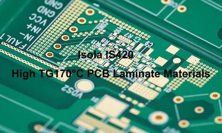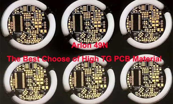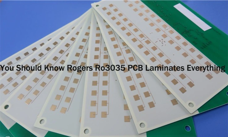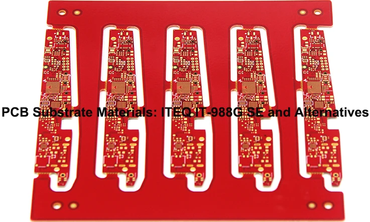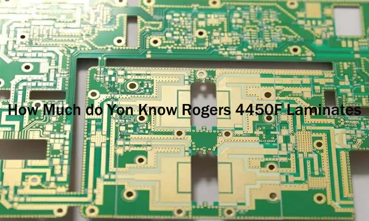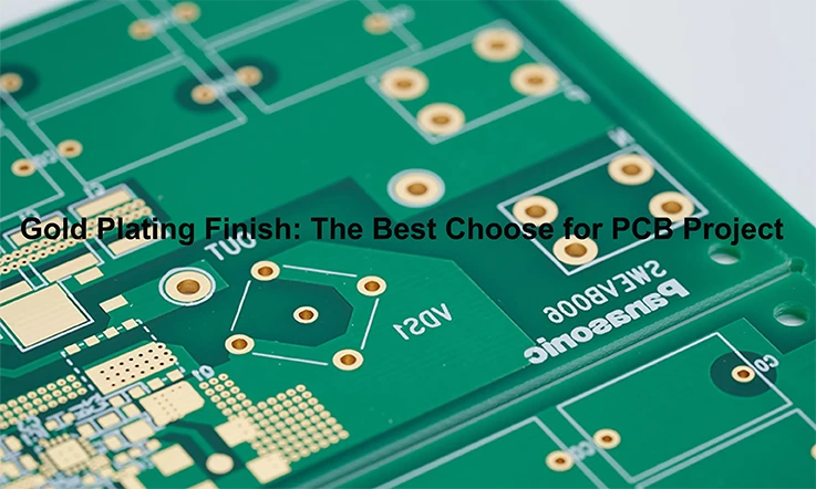
Gold plating is a renowned surface finish used in the manufacturing of printed circuit boards (PCBs) to enhance their performance, reliability, and longevity. With its superior electrical conductivity, corrosion resistance, and solderability, gold plating offers a host of benefits that make it a preferred choice in various industries. This article delves into the world of gold plating as a PCB surface finish, exploring its advantages, challenges, and how it can elevate the functionality of electronic devices.
What is Gold Plating on PCBs?
Gold plating on PCBs refers to the electrochemical process of depositing a layer of gold onto the PCB surface using an electrical current. In this process, the PCB serves as the cathode, while gold ions in a solution are attracted to and deposited onto the PCB surface under the influence of an applied electrical potential.
The thickness of the gold plating can be accurately controlled, typically ranging from 10 to 100 micro-inches. The plating is selectively applied only to specific areas of the PCB, such as contact fingers, pads, and traces that are electrically connected and require the benefits of gold plating.
By utilizing this electroplating technique, a uniform and controlled layer of gold is formed on the designated areas of the PCB. The thickness of the gold layer can be tailored to meet the specific requirements of the application, ensuring optimal conductivity, corrosion resistance, and durability.
How Gold Plating Finish Working on PCB Boards?
Gold plating finish on PCB boards is achieved through a process called electroplating. The process involves depositing a thin layer of gold onto the surface of the PCB, typically over a base layer of nickel or copper. Here is a step-by-step overview of how gold plating finish works on PCB boards:
1. Surface Preparation: The PCB surface is thoroughly cleaned and prepared to ensure proper adhesion of the gold plating. This involves removing any contaminants or oxides from the surface through processes like scrubbing, etching, and rinsing.
2. Activation: In some cases, the PCB surface may require activation to promote adhesion. This is typically done by immersing the PCB in a solution that contains a chemical activator, such as a mixture of sulfuric acid and hydrogen peroxide. The activator removes any remaining oxides and prepares the surface for plating.
3. Electroplating: Once the surface is prepared and activated (if necessary), the electroplating process begins. The PCB is immersed in an electrolyte bath containing gold ions. The PCB acts as the cathode (negative electrode), while a gold anode (positive electrode) is also present in the electrolyte bath.
4. Electric Current and Deposition: When an electric current is applied, the gold ions in the electrolyte are attracted to the PCB surface. The gold ions gain electrons and form a layer of metallic gold, which gradually builds up on the surface of the PCB. The thickness of the gold layer can be controlled by adjusting the plating time and current density.
5. Final Finishing: Once the desired thickness of gold plating is achieved, the PCB is removed from the electrolyte bath and rinsed to remove any residual chemicals. The PCB may undergo additional processes such as rinsing with deionized water, drying, and inspection to ensure the quality of the gold plating finish.
It is important to note that the specific details of the gold plating process, such as the composition of the electrolyte bath and plating parameters, may vary depending on the desired thickness and application requirements.
Overall, gold plating finish on PCB boards is a controlled electrochemical process that ensures the deposition of a thin layer of gold onto the surface. This layer provides the desired benefits such as improved conductivity, corrosion resistance, and aesthetic appeal.
Types of Gold Plating used in PCB Fabrication
There are several types of gold plating used in PCB fabrication. Here are some commonly used ones:
Electroplated Hard Gold: Electroplated hard gold, also known as Hard Gold or Hard Electrolytic Gold, is a thick layer of gold applied through an electroplating process. It offers superior durability and wear resistance, making it suitable for applications with frequent insertions and high-wear requirements, such as edge connectors and switches.
Soft Gold: Soft gold plating involves depositing a thinner layer of gold compared to hard gold. It provides good electrical conductivity and is commonly used for applications where soldering is not required, such as gold wire bonding.
Wire Bondable Soft Gold: This type of gold plating is designed specifically for wire bonding applications. It offers a controlled surface for wire bonding and provides reliable interconnections between the PCB and semiconductor chips.
Selective Gold Plating: Selective gold plating involves applying gold only to specific areas of the PCB, typically using a masking technique. It is commonly used for contact pads or connectors where gold’s superior conductivity and corrosion resistance are required.
Flash Gold: Flash gold plating is a thin layer of gold applied through electroplating or electroless plating. It is often used for applications where a minimal gold thickness is sufficient, such as low-cost consumer electronics.
It’s important to consider the specific requirements of the PCB design, including solderability, wear resistance, wire bonding capability, and cost, when selecting the appropriate gold plating method for a given application.
Benefits of Gold Plating on PCB
Gold plating on PCBs offers several benefits that make it a preferred surface finish in many applications:
Excellent Electrical Conductivity:
Gold is an excellent conductor of electricity, ensuring reliable signal transmission and minimizing electrical resistance. Gold-plated surfaces provide low contact resistance, making them ideal for applications where high-quality electrical connections are crucial.
Corrosion Resistance:
Gold is highly resistant to corrosion and oxidation, making it a reliable choice for PCBs exposed to harsh environments or moisture. Gold-plated surfaces maintain their integrity over time, preserving the functionality and reliability of the PCB.
Solderability:
Gold plating enhances the solderability of PCBs by promoting better wetting and adhesion during the soldering process. The gold layer acts as a barrier, preventing the diffusion of other metals into the solder joint and ensuring reliable solder connections.
Durability and Wear Resistance:
Gold plating provides excellent durability and wear resistance, making it suitable for applications with frequent insertions or demanding environments. Gold-plated contacts and connectors maintain their performance even after multiple mating cycles, reducing the risk of signal degradation or mechanical failures.
Excellent Surface Flatness:
Gold plating typically results in a smooth and flat surface finish on the PCB, ensuring uniform contact and reducing the risk of electrical discontinuities or signal loss. This is particularly important for applications involving fine-pitch components or high-frequency signals.
Compatibility with Wire Bonding:
Gold-plated surfaces are compatible with wire bonding techniques commonly used in semiconductor packaging. The gold layer provides a reliable surface for wire bonding, ensuring strong interconnections between the PCB and semiconductor chips.
Aesthetics:
Gold plating offers an aesthetically pleasing appearance to PCBs, particularly in consumer electronics or high-end applications where visual appeal is important.
Challenges and Limitations When Use Gold Plating in PCB Manufacturing
While gold plating offers numerous advantages in PCB manufacturing, there are also some challenges and limitations to consider:
1. Cost: Gold is a precious metal, and its cost is higher compared to other surface finishes. Gold plating can significantly increase the overall production cost of PCBs, making it less feasible for cost-sensitive applications or large-scale production.
2. Thickness Control: Achieving precise control over the thickness of the gold plating layer can be challenging. Variations in plating parameters and process conditions can result in inconsistencies in the thickness across the PCB, which may affect performance or reliability, particularly in applications with tight tolerances.
3. Surface Roughness: The gold plating process can introduce surface roughness or unevenness, especially on complex PCB designs or areas with fine-pitch components. This can pose challenges during assembly or cause difficulties in achieving proper solder joint formation.
4. Limited Solderability: While gold plating enhances solderability in most cases, it is not as compatible with all soldering processes and materials. Gold has a lower affinity for solder compared to other metals like copper or tin, which can impact solder wetting and adhesion. Proper flux selection and optimization may be required to ensure reliable solder joints.
5. Wear and Durability: While gold is generally durable, it is not as hard as some other surface finishes. In applications with high-wear requirements or where frequent contact mating cycles occur, the gold plating may experience wear or abrasion over time, potentially affecting the reliability of the PCB.
6. Environmental Concerns: Gold is a precious resource, and its extraction and disposal can have environmental impacts. Additionally, some gold plating processes may involve the use of chemicals that can be environmentally hazardous if not handled properly.
7. Limited Availability: In some regions, the availability of gold plating services may be limited, leading to longer lead times or higher costs for PCB manufacturing.
It is important to carefully evaluate the specific requirements of the PCB design and the intended application before selecting gold plating as the surface finish. Alternatives, such as gold alternatives (e.g., ENIG) or different surface finishes, should also be considered based on cost, performance, and environmental considerations.
Comparing Immersion Gold vs Gold Plating
Immersion gold and gold plating are two common surface finishes used in the electronics industry, particularly on printed circuit boards (PCBs). While both provide a layer of gold on the surface, there are some differences between them:
1.Process:
Immersion gold, also known as electroless nickel immersion gold (ENIG), is a chemical deposition process. It involves depositing a thin layer of nickel onto the copper traces of the PCB, followed by a layer of gold over the nickel. On the other hand, gold plating is an electroplating process that involves applying a layer of gold onto the PCB surface using an electric current.
2.Thickness:
Immersion gold typically provides a thinner layer of gold compared to gold plating. The gold layer in immersion gold is usually around 1-2 microinches (0.025-0.05 micrometers) thick, while gold plating can vary in thickness, ranging from a few microinches to several micrometers.
3.Solderability:
Both immersion gold and gold plating offer good solderability. However, immersion gold is known to provide better solder wetting, which means solder easily adheres to the gold surface during the soldering process. This is due to the thin layer of nickel under the gold, which acts as a barrier against oxidation.
4.Durability:
Gold plating generally offers better durability compared to immersion gold. The thicker layer of gold in gold plating provides increased resistance to wear, abrasion, and corrosion. This makes gold plating more suitable for applications where the PCB may be subject to harsh environments or frequent handling.
5.Cost:
Immersion gold is typically more cost-effective compared to gold plating. The chemical deposition process used in immersion gold requires fewer steps and materials, resulting in a lower overall cost. Gold plating, being an electroplating process, involves additional equipment, chemicals, and labor, making it relatively more expensive.
What Types of Circuit Boards Use Gold Plating Finish?
High-reliability Boards: Gold provides corrosion resistance and reliable connections for mission-critical applications like aerospace, medical, and military electronics.
High-frequency Boards: Gold has excellent conductivity and prevents signal loss at high frequencies like in RF and microwave circuits.
Boards for Harsh Environments: Gold withstands moisture, high temperatures, and chemical exposure better than other surface finishes.
Prototype and Low-volume Boards: Gold allows for repeated mating of connectors during prototyping and small batch assembly.
Connector Contacts: Gold-plated connector contacts prevent wear and provide non-corrosive connections.
Pins and Leads: Gold-plated pins, leads, and contact areas provide corrosion resistance.
High-density Interconnects: Gold allows reliable connections as interconnect density increases.
Conclusion
In the realm of PCB surface finishes, gold plating stands out as a versatile and highly beneficial choice. Its exceptional electrical conductivity, corrosion resistance, and solderability make it indispensable for applications where reliable signal transmission and long-term reliability are paramount. While challenges and limitations exist, careful consideration of cost, thickness control, surface roughness, and environmental concerns can help engineers make informed decisions.
With gold plating, PCBs can achieve optimal performance, durability, and solder joint integrity, catering to the demands of industries such as aerospace, telecommunications, medical devices, and high-end consumer electronics. By harnessing the power of gold plating as a surface finish, manufacturers can elevate the functionality and reliability of electronic devices, ensuring seamless operation and customer satisfaction.

