In the fast-paced world of PCB design engineering, surface finish plays a crucial role in ensuring optimal performance and reliability. As a PCB design engineer, selecting the appropriate surface finish is crucial to ensure the performance, reliability, and longevity of electronic devices.
Among various surface finish options, Plating Flash Gold has emerged as a popular choice due to its unique combination of functionality and aesthetic appeal. This article delves into the intricacies of Plating Flash Gold PCB Surface Finish, exploring its benefits, disadvantages, process, applications, and the design consideration. By delving into the academic and technical aspects, this article aims to provide valuable insights for PCB design engineers seeking to optimize their designs.
What Is Plating Flash Gold Surface Finish?
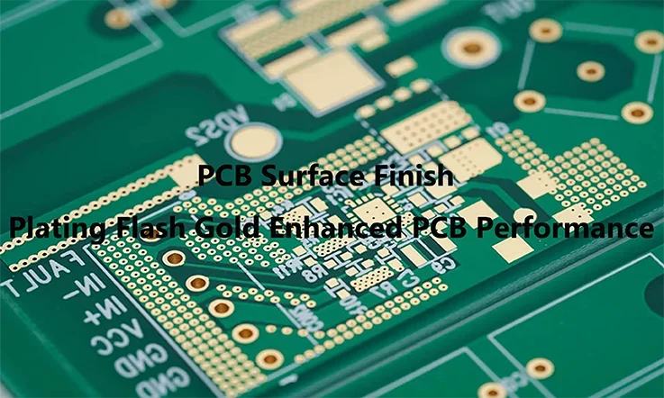
Plating flash gold surface finish, also referred to as gold plating, is a process in which a thin layer of gold is deposited onto the surface of a substrate or material. This technique is commonly used in electronic manufacturing, particularly for printed circuit boards (PCBs).
During the flash gold plating process, the substrate is prepared by cleaning and activating the surface to ensure proper adhesion. The substrate is then immersed in an electrolyte solution containing gold ions. Through the application of an electrical current, gold ions are reduced and deposited onto the surface of the substrate, forming a thin layer of gold.
The thickness of the gold layer in flash gold plating is usually relatively small, typically ranging from a few microinches to a few hundred microinches (microns). The specific thickness can vary based on the application requirements and industry standards.
Advantages and Disadvantages of Flash Gold Plating
Flash gold plating holds significant importance in various applications where a reliable and high-quality surface finish is required. Here are some key reasons why flash gold plating is important:
Advantages of Flash Gold Plating:
1.Solderability: Flash gold plating enhances the solderability of the PCB surface. It provides a uniform and smooth layer of gold that promotes excellent wetting and adhesion of solder during assembly processes. This ensures reliable and consistent solder joints, reducing the risk of solder defects such as poor wetting, solder bridging, or insufficient bonding.
2.Corrosion Resistance: The flash gold plating layer acts as a protective barrier against oxidation and corrosion. Gold is highly resistant to tarnishing and does not react readily with atmospheric elements or moisture. This helps to prevent the degradation of the underlying copper traces and ensures the long-term reliability and performance of the PCB.
3.Wire Bondability: Flash gold plating offers good wire bondability, making it suitable for applications that require wire bonding. Wire bonding is a common technique used in semiconductor packaging and microelectronics to make electrical connections between the chip and external leads or contacts. The smooth and conductive gold surface facilitates reliable wire bonding, ensuring proper electrical connections and signal integrity.
4.Contact Reliability: Gold is known for its excellent electrical conductivity and low contact resistance. Flash gold plating provides a conductive surface that ensures efficient signal transmission and minimizes signal loss or interference. It is particularly important in applications where reliable electrical contacts are crucial, such as high-frequency circuits, telecommunications, or high-speed data transmission.
5.Aesthetics and Cosmetic Appeal: Flash gold plating offers an attractive and uniform gold appearance to the PCB. This can be desirable for applications where aesthetics matter, such as consumer electronics or high-end products. The visual appeal of flash gold plating contributes to the overall perceived quality and value of the product.
6.Compatibility with Fine Pitch Components: Flash gold plating is well-suited for fine pitch components and high-density PCB designs. The thin and uniform gold layer ensures good planarity and uniform solder coverage, enabling reliable soldering of small-sized components with tight spacing. It facilitates the assembly of advanced electronic devices and miniaturized components with high precision.
Disadvantages of Flash Gold Plating:
1. Cost: Flash gold plating is generally more expensive compared to some other surface finishes, such as hot air solder leveling (HASL) or organic solderability preservatives (OSP). The cost of gold and the plating process itself contribute to the higher overall cost.
2. Limited Thickness: Flash gold plating is typically a thin layer, ranging from a few microinches to a few tenths of a micron. This limited thickness may not provide the same level of durability or wear resistance as thicker gold plating options.
3. Compatibility with Component Packages: Flash gold plating may not be suitable for all types of component packages. Certain package designs or specific components may require alternative surface finishes, such as immersion gold (ENIG) or electroless nickel/electroless palladium/immersion gold (ENEPIG), to ensure proper solderability and performance.
4. Environmental Considerations: Gold is a precious metal, and its extraction and refining processes can have environmental implications. Additionally, the disposal of spent plating solutions or waste materials containing gold requires proper handling to minimize environmental impact.
5. Risk of Whisker Formation: Gold plating, including flash gold plating, can be susceptible to the formation of microscopic metal whiskers over time. These whiskers can potentially cause short circuits or other reliability issues in sensitive applications. Careful design considerations and mitigation strategies are necessary to minimize this risk.
It’s important to note that the advantages and disadvantages mentioned above are general characteristics of flash gold plating and may vary depending on specific application requirements, process parameters, and industry standards.
Flash Gold Plating Process
The flash gold plating process involves several steps to deposit a thin layer of gold onto the surface of a printed circuit board (PCB). Here is a general overview of the flash gold plating process:
PCB Preparation:
The PCB undergoes a series of preparatory steps to ensure a clean and suitable surface for plating. This typically involves cleaning the PCB to remove any contaminants, such as dirt, oils, or oxidation, that could interfere with the plating process.
Electrocleaning:
The PCB may be subjected to an electrocleaning step, where it is immersed in an alkaline solution and an electric current is applied. This helps remove any remaining contaminants and prepares the surface for plating.
Activation:
In some cases, especially for certain substrate materials like non-noble metals or alloys, an activation step is performed. Activation involves applying a specialized chemical solution or electroless activation process to promote adhesion and prepare the surface for gold plating.
Electroplating:
The actual gold plating process is carried out using electroplating techniques. The PCB is submerged in an electrolyte solution, which contains gold ions and other additives. A direct current (DC) is applied between the PCB and an anode, typically made of gold, to facilitate the deposition of gold onto the PCB surface.
Control of Plating Parameters:
Various parameters need to be carefully controlled during the electroplating process, including the plating time, current density, temperature, agitation, and bath composition. These parameters are optimized to achieve the desired thickness and quality of the gold plating layer.
Quality Control and Inspection:
Once the gold plating process is completed, the PCB undergoes quality control measures to ensure the plating meets the required specifications. This can include visual inspection, measurement of plating thickness using specialized tools or techniques, and performing adhesion tests.
What Factors Consideration Choosing Flash Gold When Design PCB?
When considering flash gold plating as a surface finish for a PCB design, several factors should be taken into consideration. Here are some key factors to consider when choosing flash gold for your PCB design:
1. Application Requirements: Understand the specific requirements of your PCB application. Consider factors such as operating environment, expected lifespan, reliability, and performance needs. Flash gold plating may be suitable for applications requiring good solderability, corrosion resistance, and wire bondability.
2. Component Compatibility: Evaluate the compatibility of flash gold plating with the components that will be used on the PCB. Ensure that the surface finish is compatible with the component package types, such as fine-pitch components, ball grid arrays (BGAs), or surface-mounted devices (SMDs). Some component packages may have specific requirements or recommendations for surface finishes.
3. Soldering Process: Consider the soldering process that will be used during assembly. Flash gold plating is typically compatible with both leaded and lead-free soldering processes. However, it’s important to ensure that the plating thickness and quality are suitable for the specific soldering method being employed.
4. PCB Design Considerations: Take into account the design aspects that may influence the choice of flash gold plating. Factors such as PCB thickness, trace width and spacing, via and pad sizes, and impedance control should be considered. Ensure that the flash gold plating thickness and composition meet the design requirements for these parameters.
5. Cost and Budget: Evaluate the cost implications of flash gold plating. Gold is a precious metal, and the cost of flash gold plating can be higher compared to other surface finishes. Consider the budget constraints of your project and assess whether the benefits provided by flash gold plating outweigh the associated costs.
6. Industry Standards and Regulations: Be aware of any industry-specific standards or regulations that may dictate the choice of surface finish. Some industries, such as aerospace or medical, may have specific requirements for surface finishes to meet certain standards or comply with regulations.
7. Reliability and Longevity: Consider the expected lifespan and reliability requirements of the PCB. Flash gold plating offers good corrosion resistance and can provide long-term reliability. However, if the PCB will be subjected to harsh environments or extreme conditions, additional protective measures or alternative surface finishes may need to be considered.
8. Manufacturing Process Compatibility: Ensure that the chosen flash gold plating process is compatible with the manufacturing capabilities of the chosen PCB manufacturer. The plating process should align with their equipment, expertise, and quality control measures.
By considering these factors, you can make an informed decision regarding the suitability of flash gold plating for your PCB design, ensuring it meets the specific requirements of your application and manufacturing process.
Plating Flash Gold Comparison with Other Surface Finishes
To provide a comprehensive understanding, let’s compare flash gold plating with other commonly used surface finishes for PCBs:
1. Hot Air Solder Leveling (HASL):
●Advantages: HASL is a cost-effective surface finish that provides good solderability. It is suitable for standard through-hole components and offers a relatively thick and robust coating.
●Disadvantages: HASL may not be ideal for fine-pitch components due to uneven surface topography. It also lacks the corrosion resistance and wire bondability of flash gold plating.
2. Immersion Tin (ISn):
●Advantages: ISn offers excellent planarity and solderability, making it suitable for fine-pitch components. It is a cost-effective surface finish with good electrical properties.
●Disadvantages: ISn may be prone to oxidation over time and has limited shelf life compared to flash gold plating. It may require additional protection during storage and handling.
3. Electroless Nickel/Immersion Gold (ENIG):
●Advantages: ENIG provides a thin layer of gold over a layer of nickel, offering excellent solderability, corrosion resistance, and wire bondability. It is suitable for a wide range of component types and has good planarity.
●Disadvantages: ENIG is relatively more expensive than flash gold plating and may have limitations with high-temperature applications due to the potential for intermetallic diffusion.
4. Organic Solderability Preservatives (OSP):
●Advantages: OSP is a cost-effective surface finish that provides a flat and planar surface. It offers good solderability and is environmentally friendly.
●Disadvantages: OSP has limited shelf life and is more susceptible to handling and storage issues compared to flash gold plating. It offers lower corrosion resistance and may require additional protection during assembly and handling.
5. Electroless Nickel/Electroless Palladium/Immersion Gold (ENEPIG):
●Advantages: ENEPIG combines the benefits of nickel, palladium, and gold layers, offering excellent solderability, corrosion resistance, and wire bondability. It is suitable for a wide range of applications and component types.
●Disadvantages: ENEPIG is a complex and costly surface finish compared to flash gold plating. It requires additional process steps and may have limitations with high-temperature applications.
The choice of surface finish depends on various factors such as application requirements, component compatibility, cost considerations, and manufacturing processes. Flash gold plating offers advantages in terms of solderability, corrosion resistance, and wire bondability, making it suitable for applications where these characteristics are important. However, it may be necessary to consider alternative surface finishes based on the specific needs of the PCB design and intended application.
Application of Plating Flash Gold Surface Finish in PCB Industry
Plating flash gold surface finish, also known as selective hard gold plating, is widely used in the PCB (Printed Circuit Board) industry for various applications. It involves depositing a thin layer of gold onto specific areas of the PCB to enhance conductivity, provide corrosion resistance, and improve solderability. Here are some common applications of plating flash gold in the PCB industry:
Edge Connectors:
Edge connectors are commonly used in PCBs to establish electrical connections with other boards or devices. Plating flash gold is applied to the edge contacts to ensure reliable and durable connections over repeated insertions and removals. The gold layer provides excellent conductivity, resists tarnishing, and prevents oxidation.
Gold Fingers:
Gold fingers are the gold-plated contact pads found along the edge of a PCB. They are used for connecting the PCB to external devices or components, such as memory modules or expansion cards. Plating flash gold is applied to the gold fingers to prevent oxidation, ensure low contact resistance, and facilitate soldering during assembly.
High-Frequency PCBs:
In high-frequency PCB applications, such as RF (Radio Frequency) or microwave circuits, the signal integrity is crucial. Plating flash gold is often used in these circuits to maintain low-loss characteristics and improve signal transmission. The gold layer provides excellent conductivity and minimizes signal reflection and attenuation.
Selective Plating:
Plating flash gold is also employed for selective plating on specific areas of the PCB, such as critical contact points or exposed copper traces. This selective plating technique helps to protect sensitive areas from oxidation, corrosion, and wear. It ensures reliable electrical performance in demanding environments.
Harsh Environments:
PCBs used in harsh or corrosive environments, such as automotive, aerospace, or industrial applications, require robust protection. Plating flash gold offers excellent corrosion resistance, making it suitable for such environments. The gold layer acts as a barrier against moisture, chemicals, and other environmental factors that could degrade the PCB’s performance.
Fine-Pitch Components:
Plating flash gold is commonly used for PCBs with fine-pitch components, such as BGA (Ball Grid Array) or CSP (Chip Scale Package) devices. The gold layer helps to ensure good solderability and reliable electrical connections, even with the small contact areas and tight spacing between pins.
In Conclusion
flash gold plating stands as a versatile and reliable surface finish option for PCBs, offering a range of benefits for various applications. Its exceptional solderability, corrosion resistance, and wire bondability make it suitable for both standard and high-performance electronic devices.
As technology continues to advance, flash gold plating is likely to witness further developments, such as thinner plating thicknesses, alloyed formulations, and improved wire bondability. PCB design engineers should stay abreast of these advancements to leverage the full potential of flash gold plating and deliver cutting-edge electronic products. By harnessing the power of flash gold plating, designers can elevate the performance, reliability, and longevity of their PCB designs, ultimately shaping the future of electronic devices

