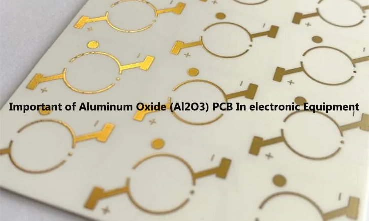
The manufacturing process of a circuit board encompasses the utilization of various materials, among which aluminum holds a prominent position in ceramic PCBs. Not only is aluminum a commonly employed material, but it also stands as the most effective choice for ceramic PCBs. In the realm of ceramic PCBs, two primary ceramic materials frequently utilized are aluminum oxide (Al2O3) and aluminum nitride (AlN).
Aluminum oxide, or Al2O3, exhibits significantly higher thermal conductivity compared to aluminum nitride, or AlN. Despite this variation, a ceramic printed circuit board remains an excellent choice for numerous applications. The specific focus of this article revolves around Al2O3 PCBs, aiming to elucidate their properties and underline their significance.
Aluminum Oxide (Al2O3) PCB Refers to Ceramic PCB or Aluminum PCB?
An Aluminum Oxide (Al2O3) PCB refers to a ceramic PCB. Aluminum oxide, also known as alumina, is a ceramic material commonly used as the base material for ceramic PCBs.
Ceramic PCBs, including those made with aluminum oxide, are designed for applications that require excellent thermal conductivity, electrical insulation, and high-temperature resistance. The aluminum oxide ceramic material provides these desirable properties, making it suitable for various electronic applications.
In an Aluminum Oxide PCB, the aluminum oxide ceramic serves as the substrate or base material for the PCB. It provides good heat dissipation capabilities, making it useful for applications that require efficient thermal management, such as power electronics, high-power LED modules, and high-frequency circuitry.
In summary, an Aluminum Oxide (Al2O3) PCB refers to a ceramic PCB that utilizes aluminum oxide as the base material. The aluminum oxide ceramic provides desirable properties such as thermal conductivity and electrical insulation, making it suitable for electronic applications requiring efficient heat dissipation and high-temperature resistance.
Aluminum Oxide (Al2O3) PCB Vs Other PCB Boards
Aluminum Oxide (Al2O3) PCBs, also known as alumina PCBs or ceramic PCBs, offer several advantages compared to other types of PCB boards. Here’s a comparison highlighting the key differences:
Thermal Conductivity:
Al2O3 PCBs have exceptional thermal conductivity, typically ranging from 20 to 30 W/MK. This high thermal conductivity allows for efficient heat dissipation, making them suitable for applications that generate a significant amount of heat. In comparison, standard FR-4 PCBs have much lower thermal conductivity, typically around 0.3 W/MK.
Electrical Insulation:
Al2O3 PCBs exhibit excellent electrical insulation properties. This makes them ideal for applications where electrical isolation is critical, such as in high-power circuits or high-voltage applications. In contrast, metal-core PCBs (MCPCBs) or standard FR-4 PCBs may not provide the same level of electrical insulation.
High-Temperature Resistance:
Al2O3 PCBs can withstand high temperatures without significant degradation. They have a high melting point of approximately 2,050°C, allowing them to operate reliably in demanding thermal environments. In comparison, FR-4 PCBs have lower temperature resistance and may experience performance issues at elevated temperatures.
Mechanical Strength:
Al2O3 PCBs exhibit excellent mechanical strength and rigidity. They have a high hardness rating, making them resistant to physical damage and providing robust support for components. On the other hand, flexible PCBs or thin FR-4 PCBs may have lower mechanical strength and are more prone to bending or damage.
Cost:
Al2O3 PCBs are generally more expensive compared to standard FR-4 PCBs due to the higher cost of alumina as a substrate material. The specialized manufacturing processes involved in producing ceramic PCBs contribute to their higher cost. However, the specific cost difference may vary depending on the size, complexity, and quantity of PCBs required.
It’s important to note that the choice of PCB material depends on the specific application requirements. While Al2O3 PCBs offer unique benefits in terms of thermal conductivity, electrical insulation, and high-temperature resistance, other PCB types like FR-4, MCPCBs, or flexible PCBs may be more suitable for applications where these particular characteristics are not crucial or where cost considerations are paramount. Ultimately, selecting the appropriate PCB board requires evaluating the specific needs of the application in terms of electrical performance, thermal management, mechanical strength, and budget.
Disavantages of Aluminum Oxide (Al2O3) PCB
While Aluminum Oxide (Al2O3) PCBs offer several advantages, they also have some disadvantages that are worth considering:
Higher Cost:
Al2O3 PCBs tend to be more expensive compared to standard FR-4 PCBs. The cost of alumina as a substrate material, as well as the specialized manufacturing processes involved, contribute to the higher price. This increased cost may be a limiting factor for budget-conscious projects or applications where cost optimization is a priority.
Brittle Nature:
Al2O3 PCBs are relatively brittle due to the ceramic nature of the material. They can be more susceptible to cracking or damage when subjected to mechanical stress or flexing. This brittleness can limit their use in applications where there is a need for flexibility or resistance to physical stress.
Limited Design Flexibility:
Compared to flexible PCBs, Al2O3 PCBs have limited flexibility. They are less suitable for applications that require bending or conforming to irregular shapes. The rigid nature of Al2O3 PCBs can restrict their use in certain design requirements or space-constrained applications.
Difficulties in Processing:
The manufacturing process for Al2O3 PCBs can be more complex and challenging compared to standard FR-4 PCBs. The specialized techniques required to work with ceramic materials may involve additional steps, such as laser drilling or specialized tooling. These factors can increase the complexity and time involved in the production process.
Limited Availability:
Al2O3 PCBs may not be as readily available as standard FR-4 PCBs since they require specialized manufacturing capabilities and expertise. This limited availability can lead to longer lead times or potential difficulties in sourcing these PCBs, especially for low-volume or custom orders.
Considering these disadvantages, it is essential to carefully evaluate the specific requirements of your application and weigh them against the advantages and disadvantages of Al2O3 PCBs. Alternative PCB materials, such as FR-4 or flexible PCBs, may be more suitable in certain situations where cost, flexibility, or ease of manufacturing are significant factors.
How Many Ways to Produce Aluminum Oxide (Al2O3) PCB?
There are several methods for producing Aluminum Oxide (Al2O3) PCBs. Here are some commonly used techniques:
Thick Film Printing:
This method involves screen printing a thick film paste containing aluminum oxide powder onto a substrate, typically using a mesh screen. The printed layers are then dried and fired at high temperatures to sinter the aluminum oxide particles and create a solid Al2O3 layer on the substrate.
Thin Film Deposition:
Thin film deposition techniques, such as physical vapor deposition (PVD) or chemical vapor deposition (CVD), can be used to deposit a thin layer of aluminum oxide onto a substrate. These processes involve vaporizing aluminum oxide and allowing it to condense onto the substrate surface, forming a thin film of Al2O3.
Tape Casting:
Tape casting is a method commonly used for producing ceramic PCBs. It involves spreading a slurry of aluminum oxide particles in a binder onto a flexible carrier film or tape. The slurry is then dried and peeled off from the carrier film, resulting in a thin, flexible sheet of Al2O3. This sheet can be laminated onto a rigid substrate and further processed to create the desired circuit pattern.
Subtractive Etching:
In this method, a thin film of aluminum oxide is deposited onto a substrate using techniques like PVD or CVD. A patterned resist is then applied on top of the aluminum oxide layer, followed by etching using chemical etchants or plasma etching. The resist protects the desired areas while the exposed aluminum oxide is selectively removed, resulting in the formation of the circuit pattern.
Laser Ablation:
Laser ablation involves using a high-power laser to selectively remove aluminum oxide material from a substrate, following a specific pattern defined by digital design files. This precise and controlled process allows for the creation of intricate circuit patterns on Al2O3 substrates.
These are just a few of the methods used to produce Aluminum Oxide (Al2O3) PCBs. The choice of production method depends on factors such as the desired thickness, complexity of the circuit pattern, cost considerations, and the specific capabilities and equipment available in the manufacturing facility.
How to Make Aluminum Oxide (Al2O3) PCB?
Making an Aluminum Oxide (Al2O3) Printed Circuit Board (PCB) involves several steps, including the creation of the Al2O3 substrate, the application of conductive layers, and the etching of the circuit design. Here’s a general overview of the process:
Substrate Fabrication
The first step is to create the base layer or substrate of the PCB. Al2O3 ceramic is often used as a substrate in high-power electronics because of its high thermal conductivity, electrical insulation, and mechanical hardness. To create the substrate, Al2O3 powder is mixed with binders and solvents to form a slurry. The slurry is then cast into a sheet, dried, and fired at high temperatures to sinter the ceramic particles together, forming a solid, rigid substrate.
Conductive Layer Deposition
Once the substrate is ready, a thin layer of conductive metal, often copper, is applied. This can be done through several methods, such as sputtering, electroplating, or lamination. The metal layer forms the basis of the electrical circuits that will be etched onto the PCB.
Circuit Design and Etching
The circuit design is then applied to the conductive layer. This can be done using a variety of techniques, including photolithography. In this process, the PCB is coated with a photoresist material, and then the circuit design is projected onto the board using ultraviolet light. This hardens the photoresist in the exposed areas. The unexposed photoresist is then washed away, revealing the metal layer beneath in the pattern of the circuit design. The exposed metal is etched away using a chemical solution, leaving only the circuit pattern.
Solder Mask Application
A solder mask is then applied over the circuitry, leaving only the contact points (pads) exposed. This helps to prevent accidental contact between the circuits during soldering.
Surface Finish
Finally, a surface finish is applied to the exposed pads to prevent oxidation and to provide a solderable surface. This could be a layer of gold, silver, or tin-lead, among others.
Component Assembly
Components are then attached to the PCB in the final assembly process. This is usually done using a soldering process, where the components are placed on the PCB and then heated to melt the solder, which cools and forms a strong, electrical connection.
Remember, this is a simplified overview of the process, and actual fabrication can be much more complex. Also, keep in mind that working with chemicals and high temperatures can be dangerous, so always follow safety guidelines and procedures.
Types of Aluminum Oxide (Al2O3) PCB
Aluminum Oxide (Al2O3), also known as alumina, is a commonly used material in the production of Printed Circuit Boards (PCBs) due to its excellent thermal conductivity, high mechanical strength, and good electrical insulation. This material is particularly suitable for high-power or high-temperature electronic applications.
There are several types of Al2O3 PCBs:
High Purity Alumina PCBs: These PCBs are made from 99.6% pure alumina. They offer excellent electrical insulation and high thermal conductivity. They are often used in high power and high-temperature electronic applications.
Low Purity Alumina PCBs: These PCBs are made from 96% pure alumina. They offer good electrical insulation and reasonable thermal conductivity at a lower cost. They are often used in lower power applications.
Alumina Ceramic PCBs: These are hybrid PCBs that use alumina ceramic as the base material and copper as the conductive layer. They offer excellent thermal conductivity and electrical insulation.
Alumina Nano-ceramic PCBs: These PCBs use alumina nano-ceramic as the base material, which provides improved thermal conductivity compared to traditional ceramics. This makes them suitable for high-power applications.
Remember, the type of Al2O3 PCB used will primarily depend on the requirements of the specific application, such as the required thermal conductivity, electrical insulation, and mechanical strength.
Properties of Alumina/Aluminum Oxide (Al2O3)
● Good gliding properties
● High hardness (15 to 19 GPa)
● Bioinert and food compatible
● Low density (3.75 to 3.95 g/cm3)
● High corrosion and wear resistance
● Moderate thermal conductivity (20 to 30 W/mK)
● Very high compressive strength (2,000 to 4,000 MPa)
● Very good electrical insulation (1×10¹⁴ to 1×10¹⁵ Ωcm)
● Operating temperature without mechanical load 1,000 to 1,500°C.
● Moderate to extremely high mechanical strength (300 to 630 MPa)
Key Applications where Alumina PCBs are Used
Power electronics – Alumina PCBs are widely used in power electronic circuits due to the high thermal conductivity and electrical insulation properties. This allows efficient thermal management in high power density devices like motor drives, power supplies, etc.
LED lighting – Alumina boards provide superior thermal dissipation which helps increase the lifespan and brightness in high-power LEDs and LED arrays.
Automotive electronics – Alumina PCBs are used in engine control units, ABS, traction control, and other automotive electronics that require high temperature tolerance.
Aerospace and defense – Alumina’s resistance to high temps and thermal shock make it ideal for avionics, radars, and other military electronics where reliability is critical.
Medical electronics – Alumina’s bioinertness allows it to be used as substrates for medical implants, surgical sensors, imaging devices, and other medical PCBs.
Laboratory analysis – The resistance to chemicals and heat makes alumina suitable for PCBs used in analytical instruments for spectroscopy, chromatography, etc.
High frequency and 5G applications – Alumina PCBs enable high frequency performance required in 5G, RF devices, antennas, and communication infrastructure.
Semiconductor manufacturing – Alumina PCBs withstand processes like plasma etching, CVD, and ion implantation in semiconductor fabs.
Oil and gas drilling – Electronics used for downhole drilling and exploration rely on alumina PCBs to survive the high temps and harsh conditions.
The unique thermal, electrical and mechanical properties allow alumina PCBs to outperform standard FR4 boards in many demanding applications.
Summary
Alumina PCBs have gained prominence as a compelling alternative to aluminum PCBs and copper-based PCBs in high-power applications. Their characteristic features, including thermal conductivity, electrical insulation properties, and mechanical strength, make them an ideal choice for demanding environments. While alumina PCBs offer several advantages, it is crucial to consider their higher cost and potential manufacturing complexities. JarnisTech stands out as a trusted provider of ceramic PCBs and assembly services, ensuring superior quality and tailored solutions for customers’ specific needs.

