8 layer PCB (Printed Circuit Board) stands at the forefront of advanced electronics, offering an excellent balance of complexity and performance. As demand for high-speed, reliable circuits grows, the multilayer 8 layer PCB find extensive use in different industries that require advanced electronic circuitry, such as telecommunicatins, aerospace, automotive, medical devices, and industrial control systems, among others. Their capability to handle faster signals, more components, and high power density allows them to meet the demands of modern electronic applications
In this article, we’ll explore the features of an eight-layer PCB and the process of its manufacturing, stack-up, Advantages, design, cost and delivery time.
Key Advantages of 8-Layer PCBs Over Traditional PCBs
When you’re designing or manufacturing electronic devices, you’re always looking for better ways to push the limits of performance. That’s where the 8-layer PCB stands out. Let’s look at how 8-layer PCBs compare to traditional PCBs, and why they’ve become the go-to choice for high-performance electronics.
1.Space Efficiency
One of the biggest perks of 8-layer PCBs is their ability to pack more functionality into a smaller form factor. With only a limited amount of space inside a device, minimizing footprint is a must. By using 8 layers, we can fit more components and make the most out of the available space. This is why 8-layer PCBs are common in compact yet powerful devices like smartphones and wearable technology.
2.Improved Signal Integrity
The way 8-layer PCBs are structured—layers of power and ground planes interspersed with signal layers—helps minimize signal loss and electromagnetic interference (EMI). In comparison to traditional single-layer or double-layer PCBs, 8-layer designs can handle much higher frequencies and ensure faster data transmission with less signal degradation. This makes them reliable for high-speed applications such as 5G communication and high-frequency processing.
3.Enhanced Power Distribution
With the addition of dedicated power and ground planes in the stack-up, 8-layer PCBs offer better power distribution. This means devices can operate more efficiently, consuming less power while maintaining stable performance. For devices that require low power consumption and high processing capabilities—such as IoT devices—this power distribution ensures they don’t overheat and continue to operate smoothly.
4.Reduced Crosstalk and Interference
The arrangement of ground planes in the 8-layer PCB stack-up helps isolate signals and reduce crosstalk—that is, unwanted interference between signals. With multiple layers dedicated to grounding, EMI is also reduced, providing cleaner and more reliable operation for high-frequency signals. This is a major advantage when compared to traditional designs, which often struggle with signal clarity.
5.High Durability and Reliability
The multilayer nature of 8-layer PCBs ensures that they can withstand harsher environmental conditions. Whether it’s temperature fluctuations or mechanical stress, these boards are designed to be more resilient than traditional PCBs, making them a best choice for applications in automotive, aerospace, and industrial environments.
6.Increased Component Density
The ability to stack more layers allows 8-layer PCBs to accommodate more components in a smaller space. This results in higher component density without taking up excessive room, which is a main factor when designing compact electronic devices that still need to deliver high performance.
The Design Process for 8-Layer PCBs
Designing an 8-layer PCB is a multifaceted process that requires a clear understanding of PCB design principles, signal integrity, and manufacturability. The complexity of multilayer PCBs calls for specific strategies to ensure the board’s layout, routing, and construction align with the desired electrical and mechanical performance.
In 8-layer PCB design, special attention is given to how the layers are stacked. This directly influences how signals propagate across the board, how power is distributed, and how heat is managed. The design process for multilayer PCBs requires thorough planning and technical expertise in these areas to achieve a design that is both effective and efficient.
Initial Design Considerations for 8-Layer PCBs
When embarking on an 8-layer PCB design, the very first consideration is the layer stack-up. The stack-up defines how the layers of the board will be arranged, typically involving signal layers and power/ground planes to create an optimal design for high-speed applications.
The layer stack-up determines the board’s ability to handle complex, high-frequency signals and ensures that power is evenly distributed across the board. By carefully selecting trace width and via types, we can achieve the right impedance for signal lines, keeping everything in line for optimal performance. A solid stack-up setup not only helps with signal integrity but also makes sure that the power flows evenly across all layers.
Below is a table outlining common stack-up configurations for 8-layer PCBs, highlighting the various layers and their general function:
| Layer | Function | Description |
| Layer 1 (Top) | Signal Layer | Carries high-speed signal traces |
| Layer 2 | Ground Plane | Provides a return path for signals |
| Layer 3 | Signal Layer | Additional signal routing layer |
| Layer 4 | Power Plane | Distributes power to the components |
| Layer 5 | Signal Layer | Additional signal routing layer |
| Layer 6 | Ground Plane | Additional ground layer for noise reduction |
| Layer 7 | Signal Layer | Additional signal routing layer |
| Layer 8 (Bottom) | Signal Layer | Carries high-speed signal traces |
Here is a visual shows the process of creating an 8 layer PCB stack up:
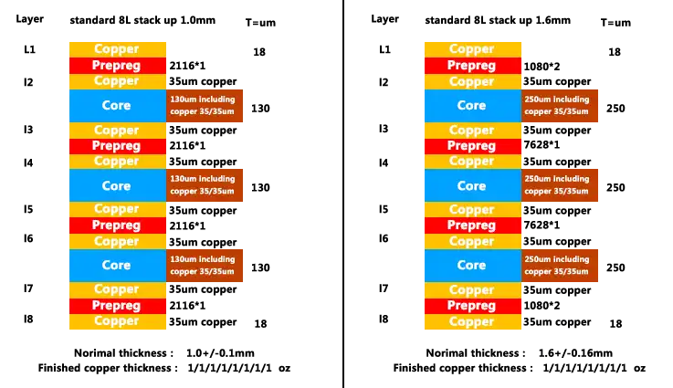
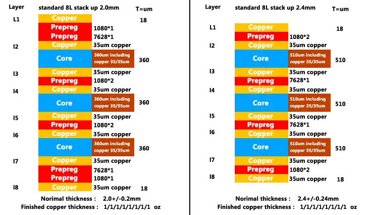
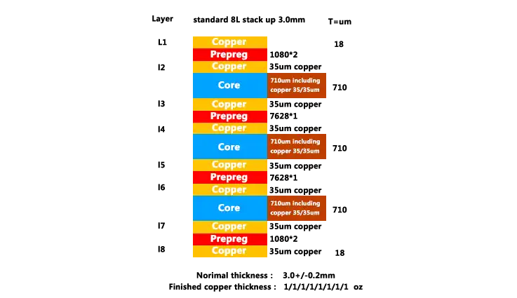
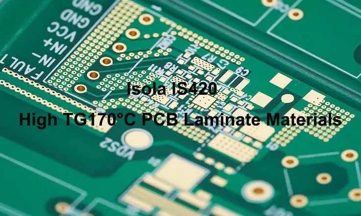
The aforementioned image outlines the design of creating an 8-layer PCB stack-up. This particular design of an 8-layer PCB stack-up is formulated considering top-tier manufacturing attributes, thereby assuring premium product quality while maintaining cost-effectiveness. For assemblies that require 8 or more layers, using a Tg170 laminate material is often the go-to choice to avoid potential quality issues during assembly.
Typically, the standard 8 layer stack-up will includes copper layers with a thickness of 1 ounce each, making it a solid option for producing multilayer PCBs. This standard setup provides a great balance between performance and manufacturability.
We also offer customization options for our clients, such as personalized stack-ups or impedance-controlled 8-layer circuit boards. If you need a copper thickness of 2oz or more, we’re happy to accommodate those requests. Just get in touch with us at [email protected] for further details.
At the heart of our service is a commitment to delivering precision-engineered PCB circuit boards and manufacturing that meet your exact specifications. We’re here to help with any questions or concerns, and we’d love to assist you in selecting the most suitable stack-up configuration for your needs.
Signal Integrity and Power Distribution in 8-Layer PCB Design
Signal integrity and power distribution are essential considerations in the design of 8-layer PCBs, particularly when handling high-frequency applications. The way you structure the layers and manage signal routing directly impacts the performance of the finished board.
One of the main advantages of an 8-layer PCB is the ability to isolate power and ground planes within the board itself. This isolation helps ensure that signals are transmitted cleanly without interference from nearby power or ground layers, especially at high frequencies. The careful arrangement of the signal layers and power planes reduces the chances of crosstalk and electromagnetic interference (EMI).
The following table demonstrates typical impedance values for signal traces in different types of 8-layer PCB designs:
| Signal Trace Type | Impedance Value | Layer Configuration |
| Single-ended signals | 50 ohms | Typically routed in outer signal layers |
| Differential signals | 100 ohms | Routed in inner signal layers |
| Power distribution (plane) | 0 ohms (ideal) | Routed in power planes |
When designing for signal integrity, the trace width and separation between traces on each layer must align with the desired impedance. If the impedance isn’t consistent, signal reflections can occur, which can lead to signal degradation.
Similarly, power distribution in 8-layer PCBs is highly optimized due to the dedicated power planes. This setup helps keep voltage drops to a minimum, ensuring that power is consistently delivered to all components across the board. By doing so, it supports stable signal performance and ensures that each part of the board operates efficiently, without interruptions.
Design for Manufacturability (DFM) in 8-Layer PCBs
Design for Manufacturability (DFM) is an essential practice when creating 8-layer PCBs to ensure that the design can be manufactured without issues and within the budget. The principles of DFM focus on making the design simpler for production, reducing errors, and improving cost-effectiveness.
One of the main aspects of DFM is selecting via types and determining trace widths. The via types used in 8-layer PCBs should be chosen based on the manufacturer’s capabilities. For example, blind vias and buried vias are often used in multilayer PCB designs but come with their own limitations and costs.
Here’s a table showing common via types used in 8-layer PCBs, along with their characteristics:
| Via Type | Description | Cost Impact |
| Through-Hole Vias | Connects all layers from top to bottom | Lower cost, but larger footprint |
| Blind Vias | Connects outer layers to inner layers | Moderate cost, used for high-density designs |
| Buried Vias | Connects only inner layers | Higher cost, best for space optimization |
| Microvias | Very small vias used in high-density boards | High cost, used for high-frequency or compact designs |
In addition, it’s important to ensure that the layer-to-layer alignment during manufacturing is precise, as any misalignment can result in signal integrity issues or even board failure. Maintaining the right trace widths, via sizes, and spacing is ensuring that our design will get optimized.
Additionally, thermal management plays a main role in DFM. 8-layer PCBs often have components that generate heat, and careful planning of thermal vias and heat sinks is required to dissipate this heat effectively. Designing for thermal efficiency ensures that high-performance designs can maintain consistent operation.
The Manufacturing Process of 8-Layer PCBs
The manufacturing process of an 8-layer PCB is a detailed series of steps that demand precision and expertise. From selecting the right PCB materials to accurately laminating the layers and ensuring the integrity of drilling, etching, and plating, every phase plays a distinct role in determining the overall quality of the board. As 8-layer PCBs find their place in industries like telecommunications, automotive electronics, and consumer devices, understanding the manufacturing process is a part of creating a high-performing product.
The construction of an 8-layer PCB requires careful attention to material selection, alignment, and precise manufacturing techniques to ensure the board meets the performance standards. Let’s take a closer look at each stage of the manufacturing process, focusing on the materials, the alignment of layers, and the steps to ensure an efficient and reliable PCB.
Materials Used in the Manufacturing of 8-Layer PCBs
The materials used in the construction of an 8-layer PCB determine its overall electrical characteristics, thermal behavior, and mechanical properties. From the base substrates to the high-performance laminates, the right materials can help ensure the board performs well in high-frequency, high-speed applications.
In 8-layer PCB manufacturing, the base substrate is typically FR-4, PTFE (Teflon), or ceramic materials, each chosen depending on the specific application requirements. For example, PTFE is often selected for applications that demand low signal loss at high frequencies, while FR-4 is commonly used for general-purpose boards.
Here’s a summary of the common materials used in 8-layer PCB manufacturing:
| Material Type | Description | Common Applications |
| FR-4 | A fiberglass-based material with moderate electrical performance | Used in general-purpose boards |
| PTFE (Teflon) | Low loss material suited for high-frequency signals | Ideal for RF and microwave applications |
| Ceramic Substrates | High thermal conductivity and mechanical strength | Used in high-power and high-performance designs |
| Polyimide | Offers excellent thermal resistance | Flexible and high-temperature applications |
The FR-4 substrate is widely used in 8-layer PCBs for most general applications. However, for designs with more complex electrical properties, PTFE or ceramic may be used to achieve the desired signal characteristics, particularly in high-frequency and high-performance scenarios.
PCB Layer Alignment and Laminating Process
Once the materials are selected, the next step in manufacturing an 8-layer PCB is the lamination process. During this stage, the individual copper layers are bonded together. The alignment of these layers needs to be precise to ensure proper electrical connections across the board. Any misalignment can lead to issues like signal interference and poor connectivity between layers, which could impact the board’s performance. Attention to detail at this point helps avoid problems down the road and ensures the board works as expected.
The process involves placing the copper layers with prepreg (resin material) between them and applying heat and pressure to bond everything together. The alignment of each layer ensures that the traces and vias are perfectly positioned, which is need for maintaining the integrity of the signals running through the board.
The lamination process works as follows:
| Step | Process | Outcome |
| Layer Preparation | Surface cleaning and preparation to promote adhesion | Ensures the layers adhere properly to each other |
| Prepreg Application | Resin material applied between copper layers | Ensures strength and electrical stability |
| Layer Alignment | Layers carefully aligned to prevent misalignment | Guarantees correct trace routing and via placement |
| Lamination | Heat and pressure applied to bond layers | Forms a durable, solid, and electrically functional PCB |
Through precision lamination, the layers are fused together in a way that preserves the electrical properties and ensures signal consistency across the entire 8-layer PCB. This step is integral to achieving the desired signal integrity and reliability in the final product.
Drilling, Etching, and Plating in 8-Layer PCB Production
After the lamination, the next phase in 8-layer PCB production involves the creation of vias, traces, and circuit paths through drilling, etching, and plating. These steps are the backbone of connecting the various layers within the PCB, allowing signals to flow seamlessly between them. . Each process requires precise equipment and technology to ensure the dimensions and alignment of the features are accurate.
Drilling is performed to create the vias (electrical connections between layers) needed for the PCB’s functionality. Once the holes are drilled, etching removes unwanted copper to form the circuit traces, and plating coats the traces and vias with copper to ensure electrical continuity.
Here’s a step-by-step overview of these processes:
| Process | Description | Purpose |
| Drilling | Create vias through the PCB layers to connect circuits | Provides electrical pathways between layers |
| Etching | Remove excess copper from the surface to define traces | Shapes the conductive paths for the PCB |
| Plating | Apply a layer of copper to the vias and traces | Ensures electrical continuity and durability |
Drilling is typically done using laser or mechanical drills to achieve precise hole sizes, while etching uses chemical processes to create the desired patterns on the PCB. Finally, plating adds copper to the drilled vias and traces to ensure they conduct electrical signals without loss.
Together, these steps make it possible to fabricate 8-layer PCBs that meet the exact requirements for signal routing, power distribution, and overall electrical performance.
Challenges in 8-Layer PCB Design and Manufacturing
Designing and manufacturing 8-layer PCBs presents a set of distinct challenges that require attention and precision. These boards are commonly used in high-speed applications, which bring their own set of design concerns. Whether it’s ensuring the integrity of signals, managing heat effectively, or balancing cost with manufacturing processes, overcoming these challenges requires careful planning. Let’s explore some of the common hurdles and ways to address them.
Managing Signal Integrity in 8-Layer PCB Designs
Signal integrity in 8-layer PCBs is an issue we need to pay close attention to. As circuits become faster and more complex, the potential for interference, distortion, and signal loss increases. Crosstalk, impedance mismatches, and noise interference are all aspects that can affect how a signal behaves on the PCB. With 8-layer PCBs typically being used in high-frequency applications, making sure signals flow cleanly and without disruptions is a must.
Maintaining signal integrity in high-speed designs requires an understanding of the layer stack-up. Each layer has its purpose, and if not carefully considered, the performance of the board can be compromised. By utilizing proper routing techniques, reducing trace lengths, and carefully choosing materials, it’s possible to design a board where the signals remain stable and consistent.
Steps to Address Signal Integrity Issues:
| Element | Action | Best Practice |
| Layer Stack-Up | Plan signal and ground layer placement | Use ground planes for better shielding and signal separation |
| Impedance Control | Manage impedance consistently across the PCB | Incorporate controlled impedance to avoid reflection and signal degradation |
| Crosstalk Control | Prevent unwanted signal coupling | Maintain adequate spacing between signal traces and use shielding methods where necessary |
| Via Design | Minimize signal disruptions caused by vias | Utilize blind or buried vias to keep signal paths clear |
Therefore, our designers should focus on creating a layer stack-up that separates high-speed signals from noisy layers, such as power or ground planes. By ensuring impedance control, they can reduce signal reflection, ensuring the signals reach their destination without unwanted interference or loss. Also, employing via-in-pad technology or blind and buried vias can reduce signal degradation, making sure the performance of the 8-layer PCB is consistent even in high-speed applications.
Thermal Management in 8-Layer PCBs
In high-performance applications, thermal management is a serious consideration.8-layer PCBs, especially those packed with complex and powerful components, can accumulate a fair amount of heat over time. If not kept in check, this heat can lead to issues like component wear or even failure, shortening the board’s lifespan.
There are multiple approaches to controlling heat on 8-layer PCBs. The right materials, along with an efficient layer stack-up, can help dissipate heat away from critical areas. Thermal vias, placed strategically across the PCB, allow heat to travel between layers, spreading it out more evenly.
Strategies for Managing Heat:
| Thermal Factor | Focus | Solution |
| Material Selection | Use materials that conduct heat well | Choose high-conductivity laminates such as PTFE for better heat dissipation |
| Layer Stack-Up | Design to ensure heat flows toward the ground plane | Arrange layers with heat-sensitive components near heat sinks or the ground plane |
| Thermal Vias | Help heat escape from heat-generating components | Use thermal vias to transfer heat from inner layers to outer layers |
| Component Placement | Place components to minimize heat buildup | Avoid clustering heat-generating components in one area |
To manage thermal stress, it’s essential to ensure high-power components are spaced out across the board. Keeping heat-sensitive components near the ground plane or heat sinks helps move heat away from sensitive areas. Thermal vias are also used to help dissipate heat from internal layers to the surface, allowing it to escape more easily.
Cost and Manufacturing Complexity of 8-Layer PCBs
When producing 8-layer PCBs, we often face higher production costs compared to simpler designs like 2-layer or 4-layer boards. The additional layers require more time for fabrication, testing, and materials, which leads to increased costs. Moreover, manufacturing a board with multiple layers demands precision and sophisticated techniques to ensure that the layers are aligned properly.
Despite the increased cost and complexity, the benefits of 8-layer PCBs—such as their compactness, high-density design, and the ability to handle high-speed signals—often justify the extra expense. However, designers must balance these benefits with cost-effective solutions to ensure the final product meets performance requirements without excessive spending.
Optimizing Costs in 8-Layer PCB Production:
| Factor | Consideration | Solution |
| Material Costs | Higher material costs for advanced substrates | Choose cost-efficient yet reliable materials without compromising quality |
| Manufacturing Time | Extra layers lead to longer fabrication times | Utilize automated manufacturing processes to reduce labor costs and production time |
| Yield Management | Increased layers can lead to lower yields | Implement Design for Manufacturability (DFM) practices to ensure a smooth manufacturing process |
| Component Selection | Advanced components can be more costly | Source components in bulk and explore alternative suppliers for better pricing |
We can reduce the costs associated with 8-layer PCBs by selecting materials that offer the right balance between performance and affordability. Using automated processes to speed up production can also help cut down on labor costs, while adhering to DFM guidelines ensures that designs are optimized for mass production. This can help increase yield and reduce the number of faulty units produced.
By finding ways to manage production complexities and optimizing material costs, we can ensure 8-layer PCBs remain both high-performing and cost-efficient.
Testing and Quality Assurance in 8-Layer PCB Manufacturing
In 8-layer PCB manufacturing, quality is everything. Whether it’s in consumer electronics, automotive systems, or medical devices, ensuring the reliability of these complex boards is non-negotiable. From the initial fabrication to final product testing, every step must be scrutinized to guarantee that the board can withstand high-frequency signals, thermal stress, and mechanical pressure. Let’s break down the steps in the testing and quality assurance process, focusing on electrical testing, defect detection, and reliability testing.
Electrical Testing and Defect Detection in 8-Layer PCBs
Electrical testing is the bedrock of ensuring that an 8-layer PCB functions as intended. When designing such intricate circuits, even the smallest error in trace routing, pad alignment, or component placement can lead to severe performance issues down the line. Fortunately, electrical testing methods have evolved to catch these issues early in the manufacturing process, before they become a larger problem.
Automated Optical Inspection (AOI) and Flying Probe Testing are commonly employed techniques for 8-layer PCB defect detection. AOI involves scanning the surface of the PCB to visually identify faults, such as missing pads or misaligned vias. Flying Probe Testing provides a more in-depth approach by probing each point on the board and ensuring there’s no electrical failure in the circuit paths.
A continuity test is done to make sure the electrical path of the 8-layer PCB is intact, checking that there are no shorts or open circuits in the connections. It’s like making sure your car’s wiring is solid before hitting the road—no surprises allowed. Another step in the testing process is impedance control, which ensures that high-speed signals run smoothly without causing issues. A 4-point probe test, for instance, can measure any impedance mismatch in critical signal paths that might mess with performance. Think of it as fine-tuning the roads to ensure your signals travel without any hiccups. If you miss this step, it’s like trying to drive through a roadblock—you’re not going anywhere fast.
By integrating these electrical testing methods into the production line, we can ensure that 8-layer PCBs meet the performance standards required for high-speed, high-density applications.
Common Electrical Testing Methods for 8-Layer PCBs:
| Test Method | Description | Benefit |
| Automated Optical Inspection (AOI) | Uses cameras to inspect PCB surface for visible defects. | Quickly detects surface-level defects like soldering issues. |
| Flying Probe Testing | Uses test probes to check connections and components on the PCB. | Detects electrical faults, shorts, and opens across the PCB. |
| Continuity Testing | Ensures the electrical path is uninterrupted and error-free. | Confirms that the PCB performs as expected under load. |
| Impedance Control Testing | Measures impedance in critical signal paths to ensure proper performance. | Ensures signal integrity for high-frequency applications. |
X-Ray Inspection for Internal Layer Integrity
While surface-level testing gets most of the attention, the real challenge in 8-layer PCB testing happens when it comes to the internal layers—those layers are where the magic happens for signal integrity and power distribution. To ensure these layers are defect-free, X-ray inspection is used to take a deep dive into the board without causing any damage. Think of it as taking an X-ray of the PCB’s insides—this method helps us spot any sneaky voids, misalignments, or other issues that could mess with performance. By using X-rays, we’re able to see through the layers and catch any problems before they cause trouble down the line.
X-ray inspection is a valuable tool for multilayer PCB testing, especially when it comes to spotting defects in the internal layers, which can be tricky to identify with traditional techniques. The process involves sending X-rays through the PCB stack-up, allowing inspectors to observe the vias, blind holes, and buried vias, even within the inner layers. For 8-layer PCBs, this method is a major step, as it makes sure that the conductive paths are aligned correctly and there are no shorts that could lead to failure. This method ensures that all the electrical paths are in top shape, ready to perform as expected.
How X-Ray Inspection Works for 8-Layer PCB Testing:
| Aspect | Description | Benefit |
| X-Ray Penetration | X-rays pass through the PCB to inspect internal structures. | Allows for non-destructive inspection of hidden internal layers. |
| Defect Detection | Detects voids, misalignment, and poor via connections. | Ensures structural integrity of internal layers. |
| Quality Control | Provides a reliable method for identifying internal defects. | Improves overall PCB quality, reducing the risk of failure. |
Reliability Testing: Thermal, Mechanical, and High-Speed Validation
In addition to electrical testing and defect detection, reliability testing plays an integral role in confirming that 8-layer PCBs can perform well under various conditions. Thermal, mechanical, and high-speed validation tests ensure that the PCB can handle the stresses it will face during operation.
Thermal testing simulates the heat cycles that a PCB will go through in its lifetime. This includes thermal cycling (repeated heating and cooling) and thermal shock (rapid changes in temperature). Both tests help to identify potential solder joint failures, component misalignment, or delamination of the layers.
Mechanical testing focuses on the ability of the PCB to withstand external forces like vibration, bending, or pressure. This is particularly relevant for 8-layer PCBs used in automotive or industrial applications, where the board may face harsh mechanical stresses.
High-speed validation tests focus on ensuring that signals remain intact as they travel at high frequencies. For these designs, trace widths and via lengths must be optimized to avoid signal loss and crosstalk. In 8-layer PCBs often feature power and ground planes strategically placed to ensure minimal interference and consistent power distribution.
Types of Reliability Tests for 8-Layer PCBs:
| Test Type | Description | Benefit |
| Thermal Testing | Simulates temperature fluctuations to detect thermal stress. | Prevents issues like solder joint failure and delamination. |
| Mechanical Testing | Assesses PCB durability under physical stress (vibration, pressure). | Ensures reliability in automotive and industrial applications. |
| High-Speed Validation | Tests the PCB’s ability to maintain signal integrity at high frequencies. | Verifies that signal transmission remains stable at high speeds. |
Prototype Multilayer 8 layer Printed Circuit Boards Prices and Delivery Time
At JarnisTech, we specialize in fast, budget-friendly, high-quality PCB prototyping services. We follow ISO9001 standards for quality management and have an in-house quality assurance team that ensures every project meets strict guidelines.
Our prototyping services are designed for speed and efficiency, delivering PCBs in just 3-7 days, depending on your specific needs. This is a clear upgrade compared to the usual 6-12 days that many other providers take.
Our squad of proficient individuals is committed to bestowing upon our clients unparalleled service quality, promptness, and precision. We employ cutting-edge prototyping methodologies and technologies to ascertain that our clients’ PCBs align with their specifications and requirements.
JarnisTech offers fast PCB prototyping at a great value, with a focus on affordability and fast turnaround. If you’re looking for a reliable, cost-effective, and time-efficient PCB prototyping partner, we’re here to help. Reach out to us today, and let’s discuss your project’s unique needs.
Why Choose Us for Fabricating 8-Layer PCBs?
When it comes to producing high-performance 8-layer PCBs, precision, reliability, and cutting-edge technology are a must. As the demand for compact, high-frequency designs increases, the quality of the PCB fabrication process can make or break a product’s functionality. At our facility, we focus on providing 8-layer PCBs that meet the rigorous standards required by industries like telecommunications, automotive, and consumer electronics. But why should you choose us over the competition?
Expertise in 8-Layer PCB Design and Manufacturing
With over 20 years of experience in PCB manufacturing, we bring a wealth of knowledge to the table. We specialize in 8-layer PCB designs, manufacturing and Assembly, ensuring that each board meets precise electrical and mechanical requirements. Whether you need a compact design for your high-speed application or a robust PCB for an automotive system, our team has the expertise to handle the most complex designs. Our extensive experience allows us to tailor designs to your specific needs, streamlining production while maintaining top-notch quality.
Advanced Technology and Equipment for 8-Layer PCB Production
We leverage the latest advancements in PCB fabrication technology to guarantee precise, efficient manufacturing. From high-precision drilling machines to automated optical inspection systems, we use state-of-the-art equipment to ensure that each 8-layer PCB is produced with accuracy and consistency. Our advanced technology helps us deliver boards that meet the highest standards for signal integrity, power distribution, and thermal performance.
Commitment to Quality and Reliability in 8-Layer PCB Fabrication
At the heart of our manufacturing process is a rigorous quality control system designed to catch any potential issues before they reach the production floor. Our team conducts comprehensive electrical testing and uses techniques like X-ray inspection to verify the integrity of every layer. With this commitment to quality, we ensure that each 8-layer PCB we produce is not only functional but also reliable under various operational conditions. From thermal cycling to mechanical stress tests, our boards are designed to withstand the toughest challenges.
Cost-Efficiency Without Compromising on Performance
We understand that cost-effectiveness is core to any project’s success, which is why we work hard to streamline our processes and offer competitive pricing for 8-layer PCBs. Our efficient production techniques allow us to keep costs down without sacrificing performance or quality. Whether you’re working on a high-volume production run or a smaller prototype batch, we’re dedicated to delivering reliable PCBs at prices that align with your budget.
Our Multi-layer PCB Manufacturing Capabilities:
| Specification | Details |
| PCB Layers | 4 to 60 Layers |
| Delivery Time | 1 Day to 2 Weeks |
| Final Board Thickness | 0.4mm to 8.2mm |
| Materials | FR4, Polyimide, Aluminum, Ceramics, PTFE |
| Tg (FR4 Multilayer PCB) | 135°C ~ 185°C |
| Aspect Ratio | 12:1 |
| HDI Stack-up | 1+N+1, 2+N+2, 3+N+3, 4+N+4…..7N7 |
| Line/Space | 2Mil / 2Mil |
| Copper Thickness | 1/3oz to 30oz |
| Surface Finish | ENIG, Immersion Silver, Plated Gold, Immersion Tin, etc. |
| Impedance Control | 5% to 10% |
| Solder Mask /Silk Screen Color | Green, Blue, Red, Yellow, White, Black |
| Quality/Test | ISO/CE/UL/IPC Class 2 / IPC Class 3 |
Innovations and Trends of 8-Layer PCBs
As the demand for 8-layer PCBs continues to grow across industries such as telecommunications, automotive, consumer electronics, and aerospace, human are exploring new ways to improve PCB design and manufacturing processes. Recent advancements in 8-layer PCB technology are paving the way for designs that are more compact, reliable, and efficient. Let’s look at some of the recent developments that are shaping the future of 8-layer PCBs.
Flexible and Rigid-Flex 8-Layer PCBs for Emerging Applications
Flexible and rigid-flex 8-layer PCBs are gaining traction as us seek to meet the growing need for flexible, compact electronic devices. These advanced designs combine the characteristics of flexible circuits with the strength and reliability of rigid boards, offering enhanced versatility and functionality for complex applications.
The main benefit of flexible PCBs lies in their ability to bend, twist, and stretch, making them suitable for compact and space-constrained devices like wearable electronics and medical implants. With rigid-flex PCBs, we can integrate flexible sections where movement is required and rigid sections where durability and stability are necessary. This hybrid approach makes these 8-layer PCBs perfect for applications in automotive systems, consumer electronics, and even aerospace.
What sets rigid-flex PCBs apart is their layer arrangement and the careful selection of materials, which provide the needed mechanical stability and electrical reliability. The design flexibility offered by these types of PCBs leads to enhanced functionality while reducing the size of the end product, all while maintaining high performance.
Key Features of Flexible and Rigid-Flex 8-Layer PCBs:
| Feature | Description | Benefit |
| Flexibility | Ability to bend and flex without losing performance | Ideal for wearables, compact electronics, and flexible displays |
| Hybrid Construction | Combines flexible and rigid sections in a single PCB | Optimizes space usage and reduces assembly complexity |
| Material Choices | Use of flexible materials like polyimide and PET | Ensures durability, flexibility, and heat resistance |
| Layer Customization | Customizable layer stack-up for specific performance needs | Provides tailored solutions for a variety of applications |
For example, automotive sensors benefit from rigid-flex 8-layer PCBs, as they allow for both high signal integrity and flexibility in designs, accommodating complex systems while keeping size and weight manageable.
3D PCB Technology: Advancements in 8-Layer PCB Manufacturing
The rise of 3D PCB technology is transforming how 8-layer PCBs are designed and manufactured. Unlike traditional 2D PCBs, which are limited by flat, linear arrangements, 3D PCB technology allows for more complex configurations, enabling us to build multilayer circuits with greater precision.
One of the most exciting developments in this field is 3D PCB printing, which enables us to print multiple layers of a PCB in a single process. This printing technology offers several advantages, including improved manufacturing speed, reduced waste, and the ability to print complex geometries without additional tooling. As 3D PCB technology matures, its potential to bring 8-layer PCBs to new applications, such as miniaturized circuits for wearable devices and medical equipment, continues to grow.
The integration of 3D PCB technology into the manufacturing process enhances the flexibility of PCB designs. For instance, 3D printing allows for embedded components, reducing the size of the final product while maintaining performance. This technology also improves the speed at which prototypes can be tested, cutting down on time-to-market for new products.
How 3D PCB Technology Supports 8-Layer PCB Manufacturing:
| Aspect | Benefit | Effect on 8-Layer PCBs |
| Layer Integration | Allows direct printing of multiple layers | Simplifies layer stacking for more precise 8-layer PCB designs |
| Design Flexibility | Enables complex geometries and configurations | Facilitates more compact, high-performance PCBs |
| Rapid Prototyping | Shortens production cycles due to faster printing processes | Speeds up design validation and testing |
| Cost-Efficiency | Reduces material waste by printing directly | Lowers costs for 8-layer PCBs in high-volume production |
The adoption of 3D PCB printing in 8-layer PCB manufacturing is changing the landscape of high-density electronic designs, allowing us to explore new possibilities without the constraints of traditional manufacturing processes. This has direct implications for industries where space is limited and performance must not be compromised.
FAQs related to 8-Layer PCBs
1. What is the maximum size for an 8-layer PCB?
The maximum size for an 8-layer PCB depends on the manufacturing capabilities, but typical dimensions range from 50mm x 50mm to 400mm x 400mm.
2. Can 8-layer PCBs be used in flexible electronics?
Yes, 8-layer PCBs can be used in flexible and rigid-flex applications, combining the multi-layer structure with flexibility for advanced designs.
3. What is the minimum trace width and spacing for an 8-layer PCB?
The minimum trace width and spacing are typically 2.5 mils (0.0635 mm), depending on the technology and capabilities of the manufacturer.
4. How does the number of layers in a PCB affect signal integrity?
Increasing the number of layers improves signal integrity by reducing cross-talk and providing better isolation between traces, making it ideal for high-frequency circuits.
5. What is the difference between a 4-layer and an 8-layer PCB?
An 8-layer PCB offers more routing options and greater signal isolation, allowing for denser circuits and better power distribution compared to a 4-layer PCB.
6. What types of connectors are typically used with 8-layer PCBs?
Connectors used with 8-layer PCBs vary depending on the application but often include micro USB, HDMI, and high-speed interconnects for data and power transmission.
7. How do you manage thermal issues in an 8-layer PCB design?
Thermal management in 8-layer PCBs is achieved through strategic layer placement, using heat sinks, and implementing thermal vias for efficient heat dissipation.
PCB Fabrication
Multilayer PCB Manufacturing & Assembly