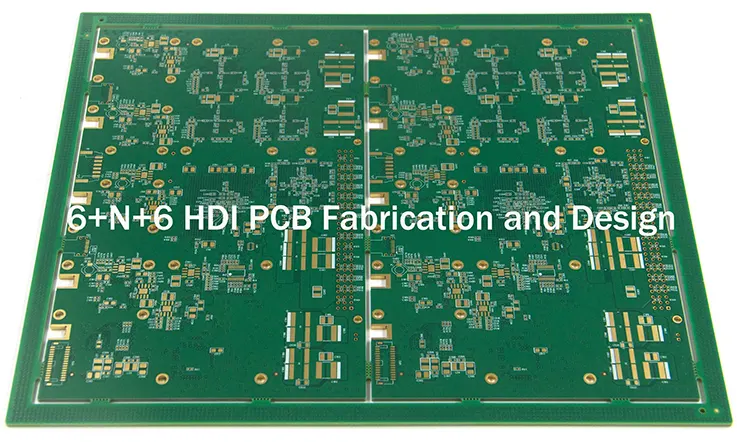
The advent of High-Density Interconnect (HDI) PCB technology has brought about a paradigm shift in the electronics industry, enabling the realization of smaller form factors and significantly increased circuit density. Among the various HDI configurations available, the 6+N+6 HDI PCB configuration emerges as an exceptional solution catering to the demands of highly sophisticated applications. Featuring a stack-up of 6 signal layers, N buried or blind via layers, and an additional 6 signal layers, this particular configuration strikes an ideal balance between complexity and functionality.
This article aims to delve into the challenges encountered when working with 6+N+6 HDI PCB and explore the innovative solutions that render them an irresistible choice for cutting-edge electronic designs.
What is 6+N+6?
In the context of HDI PCB design, “6+N+6” refers to the layer configuration of a HDI printed circuit board. It represents the arrangement of signal layers, power and ground layers, and additional signal layers within the PCB stack up.
Here’s what each component of “6+N+6” represents:
●The first “6” signifies the six signal layers. These layers are dedicated to carrying the electrical signals between different components and circuitry on the PCB.
●The “N” signifies the multiple power and ground layers. The precise number of power and ground layers can fluctuate based on the design requirment. These layers bear the responsibility for delivering an unwavering power dispersal and assuring comprehensive grounding across the PCB.
●The subsequent “6” signifies the additional signal layers. They represent extra signal layer beyond the original six signal layers. These added layers offer numerous routing flexibility and versatility for complex circuitry design.
Key Features and Benefits 6+N+6 HDI PCB
6+N+6 HDI PCB have several key features and benefits that make them suitable for advanced electronic applications.
High Density:
6+N+6 denotes the PCB’s layer stack up, encompassing six signal layers, N number of inner layers (typically power and ground planes), and an additional six signal layers. Such a layer structure accommodates a high density of interconnections, rendering it ideal for intricate and downsized electronic designs.
Increased Routing Capability:
The multitudinous signal layer found in a 6+N+6 HDI PCB yield abundant routing space, empowering the creation of complex, high speed circuits. The additional inner layers can be harnessed for power and ground planes, contributing to noise reduction and improving signal integrity.
Miniaturization:
HDI PCB are known for their ability to accommodate miniaturized components and designs. Owing to their high dense layer stack up, 6+N+6 HDI PCB facilitate the integration of tinier components and finer pitch devices, yielding more condensed and lighter electronic commodities.
Enhanced Signal Integrity:
The use of additional power and ground planes in HDI PCB helps in reducing electromagnetic interference and cross-talk, resulting in improved signal integrity. This is particularly important for high-frequency and high-speed applications.
Improved Electrical Performance:
HDI PCB, including 6+N+6 configurations, often utilize advanced materials with excellent electrical properties. These materials offer low dielectric loss, controlled impedance, and high-frequency performance, making them suitable for high-speed and high-frequency applications.
Increased Reliability:
The multi-layer structure and advanced manufacturing techniques used in HDI PCB enhance their reliability. The reduced size and shorter signal paths minimize the chances of signal degradation and improve overall system performance.
Design Flexibility:
HDI PCB offer greater design flexibility compared to traditional PCB. The increased routing capability, smaller vias, and finer trace widths allow for more complex and innovative designs, enabling engineers to optimize the performance of their electronic systems.
Applications of 6+N+6 HDI PCB
6+N+6 HDI PCB find applications in various industries and electronic devices that require high-density interconnections, miniaturization, and advanced electrical performance. Here are some common applications of 6+N+6 HDI PCB:
● Mobile Devices
● High-Speed Data Communication Systems
● Aerospace and Defense Electronics
● Automotive Electronics
● Medical Devices
● Industrial Electronics
● Test and Measurement Equipment
Design a 6+N+6 HDI PCB Steps
1. Requirements Analysis: Understand the project requirements, including the functionality, performance, size constraints, and electrical specifications of the PCB.
2. Schematic Design: Create a schematic diagram of the circuit, ensuring proper connections, component selection, and signal integrity considerations.
3. Component Placement: Assign the components within the EDA PCB design software, factoring in elements such as signal flow, thermal management and mechanical constraints. Optimize component placement for signal routing and minimize traces lengths.
4. Layer Stack up: Define the layer stack up based on the design requirements and available manufacturing capabilities. Determine the number and arrangement of signal layers, power and ground planes, and additional signal layers (N) for the HDI section.
5. Routing: Route the signal traces and power/ground connections. Pay attention to signal integrity, controlled impedance, differential pair routing, and high-speed signal requirements. Use microvias and blind vias for interconnections within the HDI section.
6. Power and Ground Planes: Create power and ground planes to ensure proper power distribution and return paths. Consider the placement of decoupling capacitors to minimize noise and voltage fluctuations.
7. Signal Integrity Analysis: Perform signal integrity analysis, including checking for impedance mismatches, cross-talk, and signal reflections. Use simulation tools to validate the design and make necessary adjustments.
8. Design Rule Check (DRC): Run a DRC to ensure compliance with manufacturing and assembly guidelines, including clearances, minimum trace widths, and annular ring sizes.
9. Design for Manufacturability: Optimize the design to enhance manufacturability, taking into account capabilities and limitations of the selected fabrication. Ensure that the design is viable to manufacture within the projected cost and timeline.
10. Gerber File Generation: Generate the Gerber files, which are the industry-standard format for PCB fabrication. Include all necessary layers, solder mask, silkscreen, and drill files.
11. Prototype and Testing: Fabricate a prototype of the PCB and perform thorough testing to validate its functionality and performance. Identify any issues or areas for improvement.
12. Iterative Refinement: Based on the results of testing and feedback, refine the design if necessary, addressing any identified issues or optimizations.
Manufacturing a 6+N+6 HDI Printed Circuit Boards Steps
1.Design: Craft a comprehensive PCB design employing computer-assisted design (CAD) software. Take into account aspects like the layer stack up, component placement, routing, and maintenance of signal integrity.
2. Material Selection: Choose the appropriate materials for your PCB, including the substrate, copper foils, and prepregs. For HDI boards, specialized materials with thin dielectrics and high-density interconnect features may be required.
3. Pre-processing: Before lamination it’s essential to clean and ready the foundational materials, like the substrate and copper foils to guarantee strong adhesion.
4.Layer Stack up: Layout the layers according to the design requirements. For a 6+N+6 HDI board, this generally implies the stack ups of numerous inner layers having high density interconnects situated between them.
5.Drilling: Precisely drill the required holes for vias, through holes, and component mounting. HDI boards often include microvias, blind vias, and buried vias to achieve high density interconnects.
6. Electroless Copper Deposition: Apply a thin layer of electroless copper to the drilled holes and exposed copper surfaces to create conductive pathways.
7. Imaging: Transfer the PCB design onto the outer layers using a process called photolithography. This involves applying a photosensitive resist, exposing it to UV light through a photomask, and developing it to create the circuit pattern.
8. Plating: Electroplate the exposed copper surfaces with additional copper to increase the trace thickness and ensure good conductivity.
9. Lamination: Use heat and pressure to bond the layers together, including the inner layers and outer copper foils. This step helps create a solid multi layer structure.
10. Etching: Remove the excess copper from the outer layers using an etching process. This leaves behind the desired copper traces and pads.
11. Solder mask Application: Apply a solder mask to protect the copper traces and define the soldering areas. This helps prevent short circuits and provides insulation.
12. Surface Finish: Apply a surface finish to protect the exposed copper surfaces and facilitate soldering. Common surface finishes include HASL (Hot Air Solder Leveling), ENIG (Electroless Nickel Immersion Gold) and OSP (Organic Solderability Preservative).
13. Silkscreen Printing: Add component designators, logos, and other markings to the PCB using a silkscreen printing process. This helps with component placement and identification.
14. Testing: Perform electrical testing to ensure the integrity of the circuit connections, including continuity, impedance and signal quality.
15. Inspection: Inspect the assembled PCB for any defects. Such as soldering issues, component misalignment, or shorts.
16. Final Testing: Conduct functional testing to verify the performance of the completed PCB.
Challenges and Solutions in 6+N+6 HDI PCB
The implementation of 6+N+6 HDI PCB technology introduces some specific challenges during the design and manufacturing stages owing to its amplified layer count and complexity. Here are some typical challenges and their corresponding solutions:
Signal Integrity:
With increasing circuit density, signal integrity becomes crucial. Potential complications such as signal crosstalk, impedance control, and power integrity may transpire. Solutions include scrupulous placement and routing of high speed signal traces, the employment of specific ground and power planes, controlled impedance routing, and the application of simulation techniques to scrutinize and enhance signal integrity.
Vias and Layer Stacking:
The presence of buried and blind vias in the 6+N+6 HDI stack up adds complexity to the manufacturing process. Challenges can include achieving reliable and precise via drilling, alignment, and plating. Solutions involve using advanced PCB fabrication techniques, such as laser drilling and precise registration systems, to ensure accurate placement and alignment of vias.
Thermal Management:
Higher circuit density can culminate in augmented heat production, consequently posing challenges for thermal management. Resolutions encompass meticulous positioning of components that generate heat, utilization of thermal vias and conductive pads for the dispersal of heat, and integration of thermal relief structures along with heatsinks whenever requisite.
Manufacturing Complexity:
The increased number of layers, vias, and smaller features in 6+N+6 HDI PCB can make the manufacturing process more complex. Challenges include precise layer alignment, registration, and lamination. This can be circumvented by employing progressive manufacturing technologies such as laser direct imaging (LDI) for refined layer alignment, automated optical inspection (AOI) mechanisms for certainty in quality, and rigid process supervision to guarantee unwavering fabrication quality.
Cost Considerations:
The complexity and higher layer count of 6+N+6 HDI PCB can result in increased manufacturing costs compared to traditional PCB technologies. Resolutions encompass enhancing the design for cost-effectiveness by curtailing extraneous layers and vias, leveraging standard materials and processes whenever feasible, and working closely with PCB manufacturers to identify cost-saving opportunities without compromising functionality.
Design for Manufacturability (DFM):
The intricate characteristics of the 6+N+6 HDI PCB necessitate careful consideration for DFM principles to guarantee both manufacturability and yield. Solutions involve close collaboration between designers and manufacturers, early DFM analysis and feedback, adherence to design rules and guidelines provided by the manufacturer, and iterative design improvements based on manufacturing feedback.
6+N+6 HDI Comparison with Other HDI PCB Technologies
When comparing the 6+N+6 HDI PCB technology with other HDI PCB technologies, it’s important to consider factors such as layer count, signal integrity, manufacturing complexity, and cost. Here’s a comparison with some other common HDI PCB technologies:
4+N+4 HDI: This particular HDI PCB category encompasses 4 signal layers, bound by N buried or blind via layers and another 4 signal layers. It delivers a balanced circuit density while maintaining relative manufacturing simplicity compared to the 6+N+6 HDI arrangement. This circuit board archetype is extensively utilized in applications where the demand for moderate density coexists with the necessity for cost efficiency.
8+N+8 HDI: This kinds of HDI PCB features 8 signal layer, an intermediate N buried or blind via layers and another 8 signal layers. It provides higher circuit density compared to 6+N+6 HDI and is suitable for more complex designs with tighter space constraints. Yet, it simultaneously escalates the complication involved in manufacturing and the increased cost.
Microvia Technology: Microvia technology is a type of HDI PCB technology that uses microvias, which are smaller in diameter compared to traditional plated-through vias. This allows for increased routing density and finer trace/space requirements. Stacking of microvias permits the realization of multilayered structures with the number of layers varying in accordance with particular design requisites. Microvia technology can synergistically work with the 6+N+6 HDI PCB Layout or other HDI types to further refine circuit density.
Sequential Build-Up (SBU) Technology: SBU technology involves building up the HDI PCB in multiple sequential steps, adding layers and vias as needed. This makes allowances for more layered counts and complex interconnect structures. With a customizable number of layers and vias tailored to the design specification, it serves as a flexible choice for attaining high circuit density.
Hence, the selection of HDI PCB technology hinges on particular design necessities such as circuit density, cost factors and manufacturing complexity. The 6+N+6 HDI layout presents a harmonious medium between density and complexity, while alternative solutions like 4+N+4, 8+N+8, microvia technology, and SBU technology cater to various design requirements.
Final Thoughts
The realm of high density interconnect technology has been forever altered by the advent of 6+N+6 HDI PCB, which effectively address the challenges associated with circuit density and complexity. Through scrupulous consideration of signal integrity, layer stacking, thermal management, manufacturing intricacies, cost factors, and design for manufacturability, these advanced PCB have set the stage for unparalleled performance in contemporary electronic apparatus.
The capacity of 6+N+6 HDI PCB to meet e complex designs without compromising reliability and efficiency positions them as a compelling option across various sectors including telecommunications, automotive and consumer electronics.
As advancements in technology persist, the continued prominence of 6+N+6 HDI PCB is all but guaranteed, shaping the future of electronics by enabling the development of smaller, more intelligent and immensely powerful devices.

