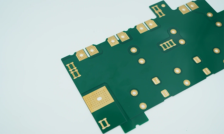
When it comes to electronic devices, handling high currents is often a challenge. A practical solution to this problem is the use of 6 oz copper PCB. This specific copper thickness is tailored to enhance the current-carrying capacity of PCB applications, ensuring efficient performance in high-power circuits.
In today’s market, JarnisTech has established itself as a reliable manufacturer of 6 oz copper PCBs. This FAQ guide will provide you with a clear understanding of the optimal design, production, property required for 6 oz copper PCB circuit boards. Let’s dive in and explore the details.
Why 6 oz Copper PCB is the Key to High-Power Circuit Success?
In the world of high-power electronics, efficiency and reliability are non-negotiable. Whether it’s driving massive power supplies, handling high currents, or managing heat in industrial equipment, 6 oz Copper PCB has carved out its niche. What sets 6 oz Copper PCB apart from standard boards is its ability to handle high-current density and thermal management in ways that other materials simply can’t. If you’re building circuits for power distribution, automotive systems, or renewable energy, then understanding the advantages of 6 oz Copper PCB is a must.
Unlike traditional 1 oz or 2 oz copper PCBs, which often struggle to maintain performance under high loads, 6 oz Copper PCB is designed to handle the heat and heavy demands of power-hungry circuits. The thicker copper layer offers a distinct advantage in industries where heat buildup and power surges are regular occurrences, making 6 oz Copper PCB a preferred choice in applications that require stable and consistent performance. Let’s dive into what makes it work.
What Sets 6 oz Copper PCB Apart in the Electronics Industry?
When you look at most PCBs, you’re dealing with a copper layer that’s anywhere between 1 oz to 2 oz per square foot. While this is sufficient for lower current applications, it quickly becomes a limiting factor as you push your designs into high-power territory. That’s where 6 oz Copper PCB makes a difference. With copper layers that are six times thicker than your standard boards, these PCBs are designed to carry more current without compromising thermal performance.
Think about it this way: if you were designing a power amplifier for an electric vehicle (EV), the last thing you want is for your PCB to overheat mid-operation. A 6 oz Copper PCB allows for much larger trace widths and better heat dissipation due to the increased copper thickness. This means higher current capacities and lower risk of thermal stress.
Here’s a quick breakdown of the difference in copper weight:
| Copper Weight (oz/ft²) | Maximum Current Capacity (A) | Typical Application |
| 1 oz | 1-2 A | Low-power electronics, signal processing |
| 2 oz | 3-4 A | Power supply circuits, moderate current handling |
| 6 oz | 10-15 A | High-current applications, automotive, power systems |
With 6 oz Copper PCB, you’re not just adding a few extra ounces of copper—you’re unlocking superior performance for high-power systems that require precise current handling and robust thermal management. The high copper content significantly lowers trace resistance, which in turn reduces voltage drop and signal degradation, resulting in a smoother, more efficient operation.
Unique Benefits of 6 oz Copper PCB for High-Current Applications
When you’re designing circuits that need to handle heavy current, whether it’s a power supply unit for a telecommunications hub or the battery management system (BMS) of an electric vehicle, you’re walking a fine line between performance and reliability. 6 oz Copper PCB is the secret weapon for pushing those boundaries.
Here’s why 6 oz Copper PCB stands out in high-current applications:
1.Superior Current Capacity: The thicker copper layer in a 6 oz Copper PCB allows it to handle high currents without risking overheating. This makes it ideal for circuits that require consistent power flow, such as in power electronics and electric vehicle charging stations.
2.Enhanced Thermal Performance: Heat is the enemy of high-current circuits. The increased copper layer helps distribute heat more effectively across the board. This leads to better thermal management, keeping components cooler for longer periods and improving overall longevity of the PCB.
3.Reduced Signal Loss: For high-speed applications like telecommunications equipment, 6 oz Copper PCB offers improved signal integrity. The lower resistance of the thicker copper layer helps maintain signal quality, even under heavy current loads.
4.Durability Under Stress: High-power systems are subject to a lot of environmental stress—from thermal cycling to vibrations. 6 oz Copper PCB is designed to endure these conditions, ensuring long-lasting reliability in industrial and automotive environments.
Key Industries Driving Demand for 6 oz Copper PCB
As industries move toward more powerful electronics and energy-efficient systems, the demand for 6 oz Copper PCB is accelerating. Automotive manufacturers, renewable energy providers, and industrial equipment makers are all turning to these robust boards to meet the growing demands of their high-power systems.
1.Electric Vehicles (EVs): As the world shifts toward electric mobility, EV manufacturers require dependable power distribution systems for their battery management systems (BMS), inverters, and motors. 6 oz Copper PCB helps to maintain stability in high-current systems, especially during charging cycles when power demands peak. For example, Tesla’s supercharging stations depend on heavy copper PCBs to effectively manage the intense power loads during fast charging sessions.
2.Telecommunications: Telecom networks require reliable power systems that can handle substantial currents without compromising signal integrity. Whether it’s for base stations or data centers, 6 oz Copper PCB ensures that power is distributed efficiently, while minimizing the risk of overheating and signal loss.
3.Renewable Energy: Solar power inverters and wind turbine controllers rely on 6 oz Copper PCB to handle large amounts of current while also maintaining optimal performance under high-stress conditions. These systems need to be durable and thermal-efficient, making 6 oz Copper PCB an reliable solution.
4.Industrial Electronics: From power distribution to heavy machinery control systems, 6 oz Copper PCB helps manage high-current systems in industrial environments. These industries demand boards that are reliable under extreme conditions—whether it’s extreme heat or high mechanical stress.
一In-Depth Analysis of 6 oz Copper PCB Design
Navigating the Complexities of 6 oz Copper PCB Design for High-Power Systems
Designing a 6 oz Copper PCB for high-power systems is far from simple; it requires a precise understanding of both electrical and thermal principles. These boards need to manage not just high currents but also the heat generated by those currents, while maintaining signal integrity and minimizing thermal stress.
In high-power applications, such as electric vehicle charging systems, solar power inverters, or industrial power supplies, careful design is must. 6 oz Copper PCB offers the necessary current capacity and thermal conductivity to meet these demands. However, achieving optimal results requires addressing aspects like trace width, impedance control, and heat dissipation—factors that directly influence the PCB’s performance and long-term durability.
Design Principles for Achieving Optimal Current Capacity in 6 oz Copper PCB
When designing a 6 oz Copper PCB, the first consideration is current capacity. With the thick copper layer, the board can carry far more current than a standard PCB, but it also comes with the challenge of handling the heat generated by that current.
To achieve the optimal current capacity, the following design principles should be prioritized:
1.Trace Width Calculations: The copper traces must be wide enough to handle the current without excessive heating. IPC-2221 standards or JESD22-A108 guidelines for trace width calculations are essential tools for us. You must account for both the copper thickness and the amount of current the board will carry, ensuring that the traces will not experience excessive voltage drop or thermal stress.
2.Minimizing Trace Resistance: Thicker copper helps reduce trace resistance, but trace length and density still play a role. For high-current applications, wider traces help lower resistance and, as a result, reduce heat buildup.
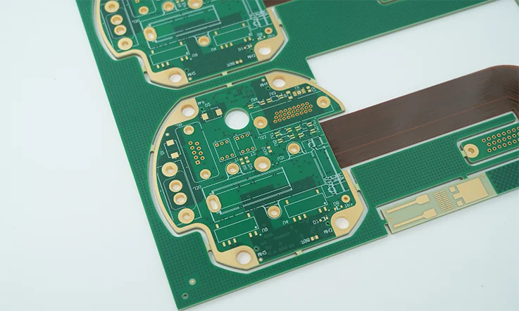
3.Designing for Flexibility: Often, 6 oz Copper PCB is used in flexible PCB applications for industries like automotive or wearables. In these designs, you’ll need to balance flexibility with current-handling capacity, requiring a careful mix of trace design and material choice.
Innovations in Trace Width and Impedance Control for 6 oz Copper PCB
When it comes to 6 oz Copper PCB, trace width and impedance control are essential. High-power systems often demand precise impedance characteristics to ensure that electrical signals travel smoothly through the board without reflection or interference.
1.Trace Widths for High Current: High currents create thermal challenges, so precise trace width calculations are essential. For example, for a 6 oz Copper PCB, you may find that a trace width of 4-5 mm (depending on the current load) is needed to safely carry 10-15 A without causing heat build-up.
2.Impedance Control: For high-speed designs, such as those used in telecommunications or data centers, impedance control ensures that the signal is transmitted efficiently across the PCB without loss. A combination of outer trace width and internal layer width must be maintained to control impedance to 50 ohms or 75 ohms depending on the application.
The layer stack-up design also plays a role in impedance control. A thicker copper layer can affect the board’s overall impedance, requiring adjustments to other factors like dielectric material and layer distribution.
Ensuring Thermal Efficiency Through Smart Design Choices in 6 oz Copper PCB
Thermal management is a significant design challenge in 6 oz Copper PCB. If heat is not managed properly, the board may fail prematurely or underperform when it’s required. Effective design can help dissipate heat efficiently, ensuring the board functions reliably in high-current environments.
1.Heat Distribution: Thermal vias and heat sinks can be used strategically to ensure heat is spread out evenly. When designing for high-current PCBs, placing vias around high-power components like MOSFETs or diodes will help direct the heat away from critical areas.
2.Thermal Simulation: Tools like ANSYS Icepak or Thermal Desktop allow our engineers to simulate how heat will be distributed across the PCB. This enables you to adjust the layout before manufacturing, ensuring optimal thermal efficiency.
3.Component Placement: Carefully consider the placement of power components on the PCB. For example, keeping high-power components further away from sensitive signal traces minimizes the risk of heat interference, which can affect signal integrity.
Common Pitfalls in Designing 6 oz Copper PCB and How to Avoid Them
Designing 6 oz Copper PCBs for high-current applications requires precision and foresight. When working with thick copper layers, there are specific challenges that must be addressed during the design process. Failure to do so can result in reduced PCB performance, overheating, and even failure in the end-use application. Below are the common design pitfalls and practical strategies to avoid them.
Thermal Mismanagement in Heavy Copper PCB Designs
Thermal management is one of core aspects of designing 6 oz Copper PCBs. Thick copper layers can carry higher currents, but this leads to increased heat generation. Without proper design considerations, heat can build up rapidly and cause component degradation or even failure.
Solution Approach:
1.Thermal Via Implementation: Ensure sufficient thermal vias to channel heat away from critical areas of the PCB. Proper placement of vias underneath high-power components like transistors or diodes enhances heat dissipation.
2.Designing with Heat Spreaders: Integrating heat spreaders or thermal pads in the PCB design aids in distributing heat over a larger surface area, which reduces the chances of localized hotspots.
3.Simulation: Use thermal simulation tools to predict the heat distribution on the PCB, enabling you to make adjustments before actual production.
Thermal Management Data Table:
| Component | Current (A) | Trace Width (mm) | Thermal Via Count | Estimated Temperature Rise (°C) |
| Power Diode | 15 | 5 | 10 | 40 |
| Power MOSFET | 20 | 6 | 12 | 45 |
| Capacitor | 10 | 3 | 8 | 35 |
| Inductor | 12 | 4 | 10 | 38 |
Note: The data above provides an estimate of the temperature rise across different components in a 6 oz Copper PCB. For accurate analysis, simulations and actual measurements are recommended.
Soldering Difficulties and How They Affect 6 oz Copper PCB Reliability
Soldering is a key process in ensuring 6 oz Copper PCB reliability, but the thickness of the copper presents unique challenges. Higher copper thickness requires increased soldering temperatures, which can lead to potential issues like cold solder joints or solder bridging if not handled correctly.
Solution Approach:
1.Preheating the PCB: Preheating is a fundamental step when working with thick copper PCBs. It allows for a more uniform temperature across the board and ensures better solder flow.
2.Specialized Soldering Equipment: Utilize high-temperature soldering irons and reflow soldering systems designed for thick copper. This helps in achieving a higher-quality solder joint.
3.Soldering Time Control: When working with 6 oz Copper PCBs, ensure that soldering time is optimized to avoid thermal stress on components. Prolonged exposure to heat can degrade the integrity of the solder joints.
Soldering Data Table:
| Soldering Method | Recommended Temperature (°C) | Time Duration (s) | Preheating Temperature (°C) | Typical Issue |
| Hand Soldering | 350 | 3-5 | 150-180 | Cold Solder Joint |
| Reflow Soldering | 240 | 5-10 | 150-180 | Solder Bridge |
| Wave Soldering | 280 | 3-5 | 120-150 | Poor Adhesion to Copper |
Note:The table above summarizes the recommended soldering temperatures and time durations for various soldering methods used with 6 oz Copper PCBs. Adjustments may be needed depending on the specific requirements of the PCB and the components being used.
Addressing Challenges in High-Current Trace Routing for 6 oz Copper PCB
Routing traces on 6 oz Copper PCBs for high-current applications requires careful planning to avoid overheating and signal loss. Thicker copper layers allow for more current-carrying capacity, but they also demand greater trace widths and careful layout to ensure proper electrical performance.
Solution Approach:
1.Trace Width Calculation: Use industry standards like IPC-2221 to calculate the correct trace widths based on current levels. It is important to balance trace width with the required thermal dissipation to ensure optimal performance.
2.Avoiding Sharp Turns: Sharp turns or angles in traces increase the electrical resistance, causing heat buildup at those points. Traces should have smooth, gentle curves to ensure current flows effectively.
3.Use of Ground Planes: A solid ground plane helps reduce noise and electromagnetic interference (EMI), especially in high-power circuits. By providing an uninterrupted return path for the current, the ground plane enhances the overall stability of the PCB.
Trace Routing Data Table:
| Current (A) | Minimum Trace Width (mm) | Trace Length (mm) | Copper Thickness (oz) | Temperature Rise (°C) |
| 10 | 3.0 | 50 | 6 oz | 25 |
| 20 | 5.5 | 100 | 6 oz | 40 |
| 30 | 7.5 | 150 | 6 oz | 55 |
| 50 | 10 | 200 | 6 oz | 70 |
Note: This table outlines the recommended minimum trace widths for various current levels, given a 6 oz Copper PCB. For accuracy, always verify with appropriate trace width calculators based on the specific PCB design.
二 Manufacturing and Quality Control for 6 oz Copper PCB
How 6 oz Copper PCB is Fabricated: A Step-by-Step Breakdown?
Fabricating 6 oz Copper PCBs requires precise control at every stage to ensure the final product can handle the high power demands. With the heavy copper layers, the fabrication process involves unique techniques compared to standard PCBs. Below is a step-by-step breakdown of how 6 oz Copper PCBs are created.
Material Selection and Sourcing for Heavy Copper PCBs
The selection of materials for 6 oz Copper PCBs is the first step in ensuring a strong foundation for high-current applications. Heavy copper PCBs require copper with high conductivity to handle the intense heat and power passing through the traces.
Material Selection Process-
●Copper Substrate: For 6 oz Copper PCBs, high-purity copper with a thickness of 6 oz (approximately 211 µm) per square foot is selected. This ensures that the copper can carry high currents without excessive heating.
●Base Layer: The PCB base material, often made from FR4 or other high-performance laminates, must be durable and thermally stable.
●Solder Mask: The solder mask is applied to protect the copper traces and prevent accidental short circuits during manufacturing.
Sourcing Materials-
●Reliable suppliers of high-grade copper foil and PCB laminates are necessary to ensure the integrity and longevity of the board. Using UL-certified materials guarantees that the final product meets industry standards for performance and safety, making it suitable for high-power applications.
Material Selection Data Table-
| Material Type | Copper Thickness (oz) | Base Material | Layer Count | Application |
| High-Purity Copper Foil | 6 oz | FR4 | 1 | High-Power Electronics |
| Copper Foil | 2 oz | Polyimide | 2 | Flexible PCBs |
| High-Conductivity Copper | 4 oz | CEM-1 | 2 | Automotive PCBs |
Etching and Plating Techniques in 6 oz Copper PCB Manufacturing
Etching and plating are vital steps in the manufacturing of 6 oz Copper PCBs. These processes shape the trace patterns that conduct electrical current throughout the board. By precisely controlling etching and plating, we can ensure that the PCB meets the required performance standards for high-current applications.
Etching Process-
●Photolithography: A light-sensitive resist is applied to the copper foil. The areas that need to be etched are exposed to ultraviolet (UV) light, creating the PCB trace pattern.
●Chemical Etching: After exposure, the PCB is submerged in an etching solution that removes unprotected copper, leaving the desired copper traces.
Plating Process-
●Electroplating: In some 6 oz Copper PCB designs, traces are plated with additional copper to increase conductivity and strength, especially in high-power applications.
●Via Plating: Plating of vias ensures electrical continuity between the layers, essential for multi-layer heavy copper PCBs.
Etching and Plating Data Table-
| Process Type | Copper Thickness (oz) | Trace Width (mm) | Plating Type | Time (minutes) | Resulting Quality |
| Photolithography | 6 oz | 0.5 | Electroplated | 10 | High Precision |
| Chemical Etching | 6 oz | 1.0 | Immersion | 15 | Smooth Edges |
| Via Plating | 6 oz | 0.3 | Gold Plating | 20 | Enhanced Durability |
How PCB Drilling and Cutting Impact 6 oz Copper PCB Quality?
Drilling and cutting are among the most physically demanding processes when it comes to 6 oz Copper PCBs, given the thick copper layers.
Drilling Process-
●Laser Drilling: For precise hole formation, laser drilling is preferred. It avoids the mechanical stresses that traditional drills may cause, ensuring that the copper layers remain intact.
●Mechanical Drilling: For larger holes, traditional drills may be used. However, the copper’s thickness requires special drilling tools and speeds to avoid creating burrs or cracks.
Cutting Process-
●Routing: The cutting of the 6 oz Copper PCB is done with CNC routers that ensure clean edges and smooth finishes. High power is required to cut through the thick copper layers without warping the material.
Impact on Quality-
●Drill Hole Cleanliness: The cleanliness and size of drill holes directly impact the reliability and integrity of the final PCB. Improper drilling can lead to issues like micro-cracks, shorts, or poor soldering connections.
●Edge Quality: The cutting process must ensure smooth, sharp edges to avoid potential issues during the assembly or use of the 6 oz Copper PCB.
Drilling and Cutting Data Table-
| Process Type | Copper Thickness (oz) | Hole Size (mm) | Drill Speed (RPM) | Quality Check |
| Laser Drilling | 6 oz | 0.2 | 20,000 | High Precision |
| Mechanical Drilling | 6 oz | 1.0 | 15,000 | Moderate Precision |
| CNC Routing | 6 oz | N/A | 12,000 | Smooth Edges |
Ensuring Quality and Durability in 6 oz Copper PCB Production
Quality control is necessary to ensure the reliability and durability of 6 oz Copper PCBs. Given the demands placed on high-power circuits, it’s essential to verify that the PCB can endure operational stresses without failure. This process helps maintain optimal performance and supports long-term functionality in a variety of applications.
Rigorous Testing Methods for High-Power PCB Durability
Testing is a vital part of 6 oz Copper PCB manufacturing. High-power electronics, especially in industries like automotive, telecommunications, and power generation, rely on rigorous durability tests.
Testing Methods-
1.Electrical Testing: It ensures all circuits are intact, with no open circuits or shorts present in the PCB. Verifying the electrical properties is essential, particularly when dealing with high-current applications..
2.Mechanical Testing: Includes tests for flexural strength, shear strength, and resistance to vibration, especially for PCBs used in mobile or automotive applications.
3.Accelerated Life Testing: Simulates long-term use to predict how the PCB will perform under normal operating conditions.
Testing Data Table-
| Test Type | Test Conditions | Target Result | Duration (hrs) |
| Electrical Testing | 5-10A current load | No open circuits or shorts | 4 |
| Mechanical Testing | 100g vibration force | No component dislodgement | 50 |
| Accelerated Life Test | 85°C, 90% RH, 10A load | No degradation of functionality | 1000 |
Importance of Thermal Stress Testing in 6 oz Copper PCB
Thermal stress testing is one of the cornerstones of validating 6 oz Copper PCBs. These boards are designed to handle heavy currents, which inevitably generate significant heat. This heat must be properly dissipated to avoid failures, especially in high-current environments.
Thermal Stress Testing-
1.Thermal Cycling: This test exposes the PCB to high and low temperatures over multiple cycles to simulate the stresses caused by temperature fluctuations in real-world applications.
2.Hotspot Testing: Identifying and measuring hotspots on the PCB allows us to take corrective action in future designs or manufacturing steps to avoid hot spots during operation.
Thermal Stress Testing Data Table-
| Temperature Cycle | Temperature Range (°C) | Cycle Time (mins) | Maximum Temperature Rise (°C) |
| Thermal Cycling | -40 to 150 | 20 | 50 |
| Hotspot Testing | 100 | 15 | 60 |
Quality Control Protocols for Ensuring Performance in High-Current Environments
To guarantee the 6 oz Copper PCB performs reliably in high-current environments, we can adhere to strict quality control protocols throughout the production process. This ensures the final product meets the required standards for performance, safety, and durability.
Quality Control Protocols-
●Incoming Material Inspection: All incoming materials, including copper foil and laminates, undergo inspection for defects before they are used in production.
●In-Process Monitoring: Each stage of the manufacturing process is monitored using automated systems to ensure consistency and quality.
●Final Inspection: The completed PCB undergoes a final inspection, where it is visually and electrically tested to ensure it meets the design specifications.
Quality Control Data Table-
| QC Stage | Testing Parameters | Frequency | Inspection Method |
| Incoming Material | Copper purity, laminate thickness | Per Batch | Visual, Microscopic |
| In-Process Monitoring | Trace width, hole diameter, copper plating quality | Every 500 units | Automated Optical Inspection (AOI) |
| Final Inspection | Functional testing, thermal stress test | Per PCB | Electrical, Thermal Analysis |
By maintaining a strict quality control process, we can ensure that 6 oz Copper PCBs consistently meet performance standards, making them reliable and durable under high-power conditions.
三 Innovative Thermal Management in 6 oz Copper PCB
Advanced Thermal Solutions for 6 oz Copper PCB in High-Power Applications
When designing 6 oz Copper PCBs for high-power applications, ensuring proper thermal management becomes non-negotiable. With the ever-increasing power demands and miniaturization of electronic devices, the 6 oz Copper PCB has become a go-to solution for handling intense heat dissipation. This section delves into the thermal solutions that can optimize performance and longevity in these high-stress environments.
Thermal performance isn’t just about keeping things cool—it’s about optimizing the heat flow to prevent thermal damage, ensure reliability, and enhance the overall design. So, how do we effectively tackle thermal management?
Copper Thickness and Its Impact on Thermal Efficiency
Copper thickness directly affects the thermal efficiency of 6 oz Copper PCBs. Simply put, the thicker the copper, the more heat the board can handle without significant thermal buildup. A 6 oz copper PCB is generally used in high-power applications where traditional PCBs fail to handle high currents.
The 6 oz thickness allows for more heat to be dissipated through conduction, reducing the likelihood of localized temperature spikes. Thicker copper also plays a key role in improving the thermal conductivity between layers, enhancing the PCB’s ability to spread heat evenly across the board. By controlling heat spread, you can maintain performance and durability even under intense loads.
Copper Thickness vs. Heat Dissipation (Data Table)
| Copper Thickness (oz) | Thermal Conductivity (W/mK) | Maximum Current Handling (A) | Applications |
| 1 oz | 380 | 5 | Consumer Electronics, LEDs |
| 3 oz | 370 | 10 | Power Supplies, High-Performance Circuits |
| 6 oz | 350 | 20 | Automotive, Industrial Electronics |
| 10 oz | 340 | 30 | Military, Aerospace, Heavy Machinery |
This table clearly shows how copper thickness influences both heat dissipation and current carrying capacity, with 6 oz copper PCBs handling significantly more power while efficiently managing heat.
Thermal Vias and Heat Sinks: The Essentials of 6 oz Copper PCB Cooling
Thermal vias and heat sinks are the bread and butter of efficient cooling in 6 oz Copper PCBs. Thermal vias provide a direct path for heat to move from one layer of the PCB to another, ensuring that excessive heat from power-hungry components can be routed away from critical areas.
By using via-in-pad technology, we can create a direct heat channel that delivers heat from the PCB surface to the back layer, where it can be dissipated more effectively. When combined with heat sinks, these solutions create an even more robust thermal management system, ensuring that 6 oz Copper PCBs remain within operational temperature ranges.
Thermal Vias and Heat Sinks Efficiency Data Table:
| Cooling Technique | Efficiency Increase (%) | Applications | Typical Use Case |
| Thermal Vias | 30-40% | Power Supplies, EV Systems | High-current connections, components |
| Heat Sinks | 50% | High-Power LEDs, Automotive | Cooling critical high-power parts |
| Via-in-Pad | 20-30% | Dense, High-power PCBs | Compact high-current PCB designs |
These solutions, paired together, offer a sophisticated method for managing thermal efficiency and ensuring your 6 oz Copper PCB can handle the heat without compromising on performance.
Strategies to Minimize Heat Accumulation in Heavy Copper PCB Designs
Reducing heat accumulation in heavy copper PCB designs involves a careful balance of material selection, board layout, and the integration of advanced cooling techniques. Here are some strategies used by top manufacturers:
1.Strategic Component Placement: By positioning high-power components in areas of the PCB where thermal dissipation is more effective, we can avoid heat concentration at sensitive points.
2.Enhanced Trace Design: Using wider traces for high-current paths minimizes the resistive heating, allowing heat to be spread across a larger surface area, significantly lowering the risk of hot spots.
3.Layer Stacking and Via Fill Techniques: By stacking layers strategically and filling vias with thermal paste or similar materials, we can create thermal channels that prevent heat buildup within any single layer.
Through careful thermal design, these strategies contribute to maintaining the integrity of the PCB and ensure it performs under heavy loads without excessive temperature rise.
Active vs. Passive Cooling in 6 oz Copper PCB Designs
When designing 6 oz Copper PCBs for high-power applications, one of the main debates is whether to use active or passive cooling methods. Both approaches offer their unique advantages and challenges, but knowing when and how to apply them can significantly improve the thermal performance and lifespan of your PCB.
Comparing Active and Passive Cooling Approaches for 6 oz Copper PCB
Active cooling involves the use of fans, pumps, or heat exchangers to actively remove heat from the PCB. It is ideal for environments where thermal dissipation demands are high, such as in power supplies for industrial equipment or high-performance electronics.
Passive cooling, on the other hand, relies on heat sinks, thermal vias, and the natural conduction of heat away from the PCB. It’s less complex and more cost-effective, making it a go-to option for less demanding applications like consumer electronics or small power devices.
Active vs. Passive Cooling Data Table:
| Cooling Type | Pros | Cons | Best For |
| Active Cooling | High efficiency, adaptable to high power | Complex, requires power and space | High-power applications, industrial systems |
| Passive Cooling | Simple, cost-effective, no additional power | Less efficient, may require larger heatsinks | Consumer electronics, mid-range power systems |
Each method has its sweet spot, and we need to weigh the pros and cons carefully to make the right choice based on the specific requirements of their project.
Integrating Cooling Solutions into the PCB Layout for Efficient Heat Dissipation
Integrating cooling solutions into the PCB layout isn’t just about slapping on a heatsink and calling it a day. To maximize heat dissipation, the PCB design must incorporate specific routing and layout strategies that enhance the flow of heat away from the components.
Best Practices for PCB Layout-
●Place heat-generating components near edges or at the back of the PCB to facilitate heat transfer away from sensitive areas.
●Use multiple layers to balance thermal load across the board, keeping the most thermally sensitive components away from high-heat zones.
Integrating these considerations early on in the design phase ensures that the 6 oz Copper PCB is both thermally and electrically optimized for high-power environments.
Designing for Thermal Balance in 6 oz Copper PCB for Maximum Longevity
Achieving a thermal balance in the PCB layout helps extend the board’s lifespan by reducing thermal fatigue. Properly managing heat distribution across the board minimizes the thermal cycling that can lead to failure in high-power environments. This is especially useful in industries like automotive or military, where durability is a top concern.
Designers can achieve thermal balance through:
●Strategic placement of thermal vias to provide optimal heat transfer.
●Use of thermal simulation software to predict heat flow and balance the design before manufacturing.
Proper thermal balance prevents heat accumulation and promotes efficient operation throughout the life of the 6 oz Copper PCB.
四 Reliability and Durability of 6 oz Copper PCB
Ensuring Long-Term Performance in Harsh Industrial Environments with 6 oz Copper PCB
When it comes to high-power applications, the reliability and durability of the 6 oz Copper PCB are non-negotiable. In industries such as automotive, aerospace, and industrial electronics, these PCBs are often subjected to extreme conditions, including high currents, high temperatures, vibrations, and environmental stresses. This section will explore how the 6 oz Copper PCB stands up to these tough environments and how it can be engineered to withstand the rigors of high-demand applications.
The ability of 6 oz Copper PCB to perform reliably under such circumstances isn’t simply a matter of raw material quality; it’s also about design strategies, manufacturing techniques, and testing protocols that ensure these boards continue to operate efficiently even in the harshest conditions.
The Impact of Environmental Stress on 6 oz Copper PCB Durability
In industrial settings, environmental stress heavily influences the lifespan of 6 oz Copper PCBs. Factors like high temperatures, humidity, chemical exposure, and mechanical stress can cause gradual wear and tear. Under extreme conditions, the repeated expansion and contraction of materials can result in micro-cracks and delamination, weakening the PCB’s structure.
To combat these issues, designers focus on:
●Material Selection: Choosing high-quality copper and specialized substrates that can handle thermal cycling and chemical exposure.
●Layering Techniques: The use of multi-layer PCBs helps distribute heat more evenly, preventing localized hotspots.
●Protective Coatings: Conformal coatings and potting materials can shield the PCB from moisture and corrosive elements.
Environmental Stress and Durability Data Table:
| Environmental Factor | Impact on 6 oz Copper PCB | Mitigation Techniques | Applications |
| High Temperature | Thermal expansion, delamination | Use of high-temperature laminates | Automotive, Power Supplies |
| Humidity | Corrosion, dielectric breakdown | Conformal coatings, moisture barrier | Aerospace, Military Electronics |
| Chemical Exposure | Material degradation, corrosion | Use of resistant materials, coatings | Industrial Equipment |
By carefully addressing these stress factors, 6 oz Copper PCBs can maintain high performance and durability in environments that would otherwise compromise lesser designs.
Preventing Failure in High-Current and High-Voltage Applications with 6 oz Copper PCB
The 6 oz Copper PCB is designed to carry higher currents and manage higher voltages, which places additional stress on the board compared to typical PCBs. As power demands increase, it’s essential to avoid issues such as thermal runaway, electrical arcing, and voltage breakdown. To prevent these failures, we can apply several strategies:
1.Trace Design and Layout Optimization: By using wider traces, 6 oz Copper PCBs can carry more current without overheating, reducing the risk of thermal damage.
2.Voltage Control: Proper isolation of high-voltage traces and the use of dielectric materials rated for higher voltages ensure that electrical breakdown is minimized.
3.Vibration Resistance: In environments with mechanical stress, special attention is given to ensuring the PCB can handle vibrations without loosening connections or causing failures.
Failure Prevention Techniques Data Table:
| Failure Type | Potential Causes | Prevention Measures |
| Thermal Runaway | Overheating due to insufficient heat dissipation | Use of wider copper traces, heat sinks, thermal vias |
| Electrical Arcing | High voltage causing arc between traces | Voltage isolation, robust dielectric material |
| Delamination/Cracking | Thermal cycling or mechanical stress | Multi-layer designs, flexible substrates |
These methods provide a comprehensive approach to ensuring that 6 oz Copper PCBs stay reliable, even in the toughest high-power environments.
The Role of 6 oz Copper PCB in Automotive and Aerospace Systems
The 6 oz Copper PCB is essential in industries such as automotive and aerospace, where reliability is a must. In these high-demand sectors, the PCB must endure extreme temperatures and perform consistently, even under conditions of vibration, shock, and electromagnetic interference.
●In the automotive industry, for instance, 6 oz Copper PCBs are used in power control units (PCUs), battery management systems, and electric drivetrains. These applications require a PCB that can withstand high currents, intense thermal loads, and vibrations from road conditions.
●In aerospace, 6 oz Copper PCBs are used in avionics and power distribution systems, where they face not only high power demands but also the challenges of high altitudes and extreme temperatures.
By using high-reliability materials and adhering to stringent quality standards, 6 oz Copper PCBs ensure that automotive and aerospace systems continue to operate reliably even under the harshest conditions.
Evaluating the Lifespan and Maintenance Needs of 6 oz Copper PCB
The longevity of 6 oz Copper PCBs often reflects their design, manufacturing process, and the environment they operate in. Proper assessment and upkeep are necessary to ensure these PCBs remain effective over time, particularly in high-power and high-stress conditions.
This section will explore how to assess the lifespan of 6 oz Copper PCBs and the best practices for maintenance to ensure that these boards remain effective and durable throughout their operational life.
Predicting Failure Modes in 6 oz Copper PCB for High-Power Systems
When assessing the longevity of 6 oz Copper PCBs, it’s essential to understand the potential failure modes that could arise under high-power conditions. Predicting these issues before they cause problems can save time, money, and reduce downtime. Here’s a breakdown of the most common failure modes found in these heavy copper PCBs:
●Thermal Fatigue: Caused by repeated thermal cycles, leading to cracks and delamination.
●Copper Migration: High currents can lead to electrochemical migration, resulting in trace failures.
●Mechanical Stress: Over time, vibration and physical stress can weaken solder joints and traces, leading to intermittent failures.
To predict these failures, we can use advanced simulation software and accelerated life testing to simulate environmental conditions over extended periods.
Preventative Maintenance for 6 oz Copper PCB in Long-Term Applications
Preventative maintenance is a proactive approach to ensuring the long-term performance of 6 oz Copper PCBs. Regular inspections and tests can detect early signs of failure, such as:
●Visual Inspection: Checking for cracks, discoloration, or other signs of heat stress.
●Electrical Testing: Conducting resistance and continuity tests to check for degradation in traces or connections.
●Thermal Testing: Monitoring temperature variations to ensure that heat is being dissipated properly.
By setting up regular maintenance schedules and keeping detailed performance logs, we can identify potential issues early and take corrective action before failures occur.
Enhancing the Service Life of 6 oz Copper PCB through Smart Design and Manufacturing
To extend the service life of 6 oz Copper PCBs, human are increasingly turning to smart design techniques that reduce stress on the board. This includes:
1.Minimizing Thermal Cycling: Using multi-layer designs and high-thermal conductivity materials to evenly distribute heat across the board.
2.Improving Material Selection: Opting for high-performance laminates and copper alloys that resist oxidation and thermal fatigue.
3.Advanced Manufacturing Processes: Leveraging automated inspection and quality control protocols to identify potential issues early in the production process.
Through these innovations, the 6 oz Copper PCB can provide years of reliable service in high-power applications.
FAQ & 6 oz Copper PCB
1. Can 6 oz Copper PCBs be used for both through-hole and surface mount components?
Yes, 6 oz Copper PCBs are compatible with both through-hole and surface-mount components, although design considerations for pad sizes and trace widths must be adjusted for thicker copper.
2. How does the weight of copper in a PCB affect its flexibility and rigidity?
The higher the copper weight, like 6 oz, the less flexible the PCB becomes. This is because thicker copper layers add rigidity, making the board less suitable for flexible applications unless special techniques are used.
3. How does the design of a 6 oz Copper PCB influence its impedance?
A thicker copper layer, like that in a 6 oz Copper PCB, can affect the impedance, especially in high-frequency circuits. Proper design ensures that impedance is controlled through the selection of trace width, copper weight, and dielectric materials.
4. Is it possible to prototype 6 oz Copper PCBs before full-scale manufacturing?
Yes, it’s possible to prototype 6 oz Copper PCBs in small batches. However, due to the more complex process involved, prototyping may take longer and be slightly more expensive compared to standard copper PCBs.
5. What are the common methods to reduce copper oxidation in 6 oz Copper PCBs?
To reduce copper oxidation, 6 oz Copper PCBs often use processes such as surface finish options (ENIG, HASL), conformal coating, or gold plating to protect the copper from environmental damage over time.
6. How do 6 oz Copper PCBs perform in high-frequency circuits?
While 6 oz Copper PCBs excel in high-power and high-current applications, they are generally not ideal for high-frequency circuits due to the potential for signal distortion caused by the thicker copper traces. Special design considerations are required for such applications.