3 oz copper PCBs stand out in the world of power electronics due to their remarkable thermal performance and enhanced ability to handle high currents. These printed circuit boards are engineered to excel in demanding environments, where heat dissipation and electrical reliability are non-negotiable. Designed with thicker copper layers, 3 oz copper PCBs support efficient thermal management, making them suitable for applications ranging from industrial machinery to high-power electronics in automotive systems.
This guide provides in-depth insights into the manufacturing processes, design considerations, and performance benefits of 3 oz copper PCBs. As we explore the latest techniques in high-temperature resistance, signal integrity, and automated production, you’ll gain a clearer understanding of why these boards are a reliable solution for industries requiring both durability and precision.
Therefore, if you’re working in the manufacturing of power supplies or designing complex circuits for electric vehicles, this guide will provide valuable information on how 3 oz copper PCBs can meet your specific needs.
Introduction to 3 Oz Copper PCBs
A Reliable Choice for High-Power Electronics
When designing high-power electronics, one of the first considerations is the material used for the printed circuit boards (PCBs). As electronics continue to evolve and demand for power grows, 3 oz copper PCBs have become a dependable solution for systems that require efficient heat dissipation and strong current-carrying capacity. These boards are specifically designed to perform under high current and power-demanding conditions, offering both mechanical reliability and effective thermal management.
In this section, we’ll break down how 3 oz copper PCBs work, why their copper thickness is a vital aspect of their functionality, and how they are applied in various real-world systems.
What is a 3 Oz Copper PCB?
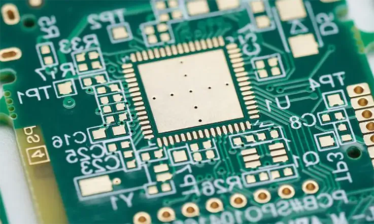
A 3 oz copper PCB refers to a printed circuit board that utilizes 3 ounces of copper per square foot (oz/ft²). This specific copper weight translates to a thicker copper layer, making it ideal for high-power applications where heat dissipation and current handling are primary concerns. The thickness of the copper directly affects how much electrical current the PCB can carry, as well as how well it can distribute heat away from critical components during operation.
In comparison to standard PCBs, which typically use 1 oz/ft² copper, 3 oz copper PCBs offer superior performance in situations where components are exposed to heavy power loads and require efficient heat transfer. The thicker copper layers allow these boards to handle greater electrical stress while also offering a more effective means of managing the heat generated by high-power components.
This makes 3 oz copper PCBs a practical choice in industries that demand robust and reliable circuit board solutions. From power supplies to LED systems, these PCBs ensure that the overall system can function without the risk of overheating or electrical failure.
The Role of Copper Thickness in PCB Design
Copper thickness plays a direct role in how efficiently a PCB manages heat and conducts electrical power. As the thickness of the copper increases, so does the current-carrying capacity and thermal dissipation potential of the board. In a 3 oz copper PCB, the additional copper allows the board to handle more current, which is necessary for applications where power flow is high and consistent.
1.Thermal Dissipation: Copper is an excellent conductor of heat, which makes it essential in high-power electronics where excessive heat can lead to component failure. With a 3 oz copper PCB, the copper layer helps spread heat evenly across the board, preventing hot spots that might cause damage to sensitive components. This design feature becomes especially useful in high-power systems, where managing heat properly can directly influence how long the device lasts and how reliably it operates under load.
2.Increased Current Carrying Capacity: The thicker copper layer allows 3 oz copper PCBs to carry higher currents than standard boards. In applications such as industrial power supplies or electric vehicle systems, handling high electrical loads without causing excessive heat buildup is a primary concern. Thicker copper ensures that power is distributed evenly across the board without stressing individual traces, thus improving overall system performance.
3.Improved Signal Integrity: 3 oz copper PCBs are also effective in systems that require clean signal transmission. While thicker copper enhances the ability to carry current, it can also improve signal clarity in high-frequency applications. The reduced resistance in thicker traces leads to lower signal loss, making these PCBs suitable for applications in RF (radio frequency) systems and high-speed circuits.
By adjusting the copper thickness and employing precise manufacturing techniques, 3 oz copper PCBs are designed to meet the specific needs of high-power systems while also maintaining efficiency and thermal control.
Applications of 3 Oz Copper PCBs in High-Power Electronics
The versatility of 3 oz copper PCBs makes them a reliable choice in a variety of high-demand applications. Their ability to manage high currents and efficiently dissipate heat makes them indispensable in industries where power density is significant. Here are a few examples where 3 oz copper PCBs are utilized:
1.Power Supplies: 3 oz copper PCBs are commonly used in power supply units (PSUs) for industrial machinery, servers, and renewable energy systems. These applications often involve high current and constant power flow, which require effective heat management. With the added thickness of copper, these PCBs ensure that power is distributed effectively, and heat is managed properly to maintain stable operations.
●Example: In high-efficiency power converters, 3 oz copper PCBs handle the electrical demands of various components, including capacitors, transistors, and inductors, without compromising the system’s overall performance.
2.LED Lighting Systems: In LED lighting systems, heat is a constant concern. LEDs generate heat during operation, and if not properly managed, this heat can affect the lifespan and performance of the LEDs. 3 oz copper PCBs provide superior heat dissipation capabilities, ensuring that the LED drivers can maintain optimal temperatures while operating under high power.
●Example: LED street lights use 3 oz copper PCBs to ensure that the heat from the high-powered LEDs is efficiently transferred to the environment, maintaining both performance and durability in harsh outdoor conditions.
3.Electric Vehicles (EVs): With the rise of electric vehicles, 3 oz copper PCBs have found a home in battery management systems (BMS) and charging circuits. These systems require high-current capacity to manage the power flow between the battery and the electric motor. 3 oz copper PCBs ensure that these systems can operate efficiently without risking overheating or power loss.
●Example: EV battery chargers use 3 oz copper PCBs to ensure the fast and safe charging of electric vehicle batteries, which need to handle large amounts of power without causing excessive thermal buildup.
These are just a few of the many applications where 3 oz copper PCBs help enhance system performance by managing high-power demands and maintaining thermal stability. Whether in industrial equipment, lighting systems, or electric vehicles, these PCBs provide a practical solution for the ever-growing demand for powerful, reliable electronics.
Key Benefits of 3 Oz Copper PCBs
Performance, Reliability, and Cost-Effectiveness
3 oz copper PCBs have gained popularity in the industry due to their outstanding performance in high-power electronics. The added thickness of the copper in these PCBs offers significant advantages when it comes to thermal management, high current handling, and cost efficiency in large-scale manufacturing. In this section, we’ll examine the specific benefits of 3 oz copper PCBs and how these advantages make them a preferred choice for demanding applications.
Thermal Management and Heat Dissipation in 3 Oz Copper PCBs
3 oz copper PCBs excel at thermal management thanks to the increased copper thickness. The thicker copper layers enhance the dissipation of heat generated by high-power components, allowing the system to maintain stable operation over extended periods of use.
●Heat Transfer Efficiency: With 3 oz copper, the board can handle the thermal load much more effectively. The heat generated from high-power components can be spread evenly across the copper surface, reducing the chances of hot spots that could damage sensitive areas.
●Thermal Resistance Comparison: Copper’s high thermal conductivity allows 3 oz copper PCBs to achieve lower thermal resistance compared to boards with thinner copper layers. This results in better heat flow away from heat-sensitive components, enhancing the overall thermal performance.
| PCB Type | Copper Thickness | Thermal Resistance (°C/W) | Heat Dissipation Efficiency |
| 1 oz Copper PCB | 1 oz/ft² | 0.50°C/W | Moderate |
| 2 oz Copper PCB | 2 oz/ft² | 0.30°C/W | Improved |
| 3 oz Copper PCB | 3 oz/ft² | 0.20°C/W | High |
As shown in the table, 3 oz copper PCBs significantly lower thermal resistance compared to 1 oz and 2 oz copper boards. This allows heat to dissipate more efficiently, which is particularly helpful in high-power electronics where heat buildup can affect performance and shorten the lifespan of the components.
High Current Carrying Capacity of 3 Oz Copper PCBs
Another significant advantage of 3 oz copper PCBs is their ability to handle high currents. The additional copper thickness increases the current-carrying capacity, making these boards ideal for power-intensive applications that require reliable current distribution.
●Current Carrying Capacity: With 3 oz copper, the PCB can handle greater electrical loads without risking trace damage or excessive heating. This increased copper thickness ensures that high currents flow through the board without compromising its integrity.
●Comparison of Current Capacity: The following table shows the increase in current-carrying capacity between different copper thicknesses. The higher the copper thickness, the greater the current load the PCB can manage.
| PCB Type | Copper Thickness | Current Carrying Capacity (A) | Heat Generation (W) |
| 1 oz Copper PCB | 1 oz/ft² | 3 A | 5 W |
| 2 oz Copper PCB | 2 oz/ft² | 6 A | 9 W |
| 3 oz Copper PCB | 3 oz/ft² | 10 A | 12 W |
As we can see, 3 oz copper PCBs can handle up to 10 amps of current, compared to the 3 amps carried by 1 oz copper PCBs. This makes 3 oz copper PCBs ideal for circuits that require higher current loads, such as industrial equipment or high-power motor controllers.
Cost Efficiency of 3 Oz Copper PCBs in Large-Scale Production
Despite the increased copper thickness, 3 oz copper PCBs offer a cost-efficient solution for industries requiring high-performance PCBs. The benefits provided by these boards—thermal management, current capacity, and material efficiency—outweigh the costs in many large-scale production environments.
●Material Efficiency: While the copper content increases with 3 oz copper PCBs, this material is effectively used to create high-performance boards. The improved current handling and heat dissipation capabilities reduce the need for expensive additional cooling systems, ultimately lowering overall system costs.
●Cost Comparison: The table below compares the material and production costs of PCBs with varying copper thicknesses. It shows that 3 oz copper PCBs provide an effective balance between cost and performance.
| PCB Type | Copper Thickness | Material Cost ($/sq ft) | Production Cost ($/unit) | Manufacturing Efficiency |
| 1 oz Copper PCB | 1 oz/ft² | $3.50 | $10.00 | Moderate |
| 2 oz Copper PCB | 2 oz/ft² | $5.00 | $12.50 | Improved |
| 3 oz Copper PCB | 3 oz/ft² | $6.50 | $14.00 | High |
From the table, we can observe that although 3 oz copper PCBs cost more per square foot, they deliver greater efficiency and longer lifespans. The increased reliability and thermal performance of these PCBs can lead to lower operational costs over time, making them a best choice for large-scale production.
Design Considerations for 3 Oz Copper PCBs
Precision, Efficiency, and Thermal Optimization
Designing 3 oz copper PCBs for high-power applications requires a thorough understanding of precision, efficiency, and thermal optimization. As electronics continue to demand higher performance, it’s necessary to design heavy copper PCBs that manage high currents effectively while ensuring efficient power distribution and adequate heat management. In this section, we’ll explore the factors that influence the design of 3 oz copper PCBs, such as the copper layer thickness, the role of impedance control, and thermal simulation for power electronics systems.
Copper Layer Thickness and Its Impact on Design Efficiency
The thickness of the copper layer is a core factor in the design of 3 oz copper PCBs. A thicker copper layer, such as 3 oz copper, helps with both power handling and thermal performance. It provides better current handling and reduces power loss through the traces, improving the overall power efficiency of the system.
●Power Efficiency: Thicker copper layers lower the resistance of the PCB traces, which directly reduces voltage drops and power loss over the length of the PCB. This ensures that the system operates more efficiently and can handle higher current loads without compromising performance.
●Thermal Management: The thicker copper helps with heat distribution, spreading the heat generated across the PCB and preventing hot spots. With more copper available, the heat is more evenly dissipated, which is especially beneficial for high-power electronics.
| PCB Type | Copper Thickness | Thermal Resistance (°C/W) | Power Loss (W) | Current Carrying Capacity (A) |
| 1 oz Copper PCB | 1 oz/ft² | 0.50°C/W | 10 W | 5 A |
| 2 oz Copper PCB | 2 oz/ft² | 0.35°C/W | 7 W | 8 A |
| 3 oz Copper PCB | 3 oz/ft² | 0.20°C/W | 4 W | 12 A |
The table demonstrates how 3 oz copper PCBs stand out in terms of thermal resistance and current carrying capacity compared to thinner copper options. This makes them well-suited for applications where high power is involved.
Achieving Low Impedance and High-Quality Signal Integrity
In power electronics, particularly for high-frequency circuits, maintaining a stable signal is a must.3 oz copper PCBs help achieve low impedance and stable signal performance by reducing the resistance of traces, which could otherwise introduce signal noise or distortion.
●Impedance Control: Thicker copper layers help ensure that the PCB traces maintain consistent impedance. The 3 oz copper PCB offers a more stable path for signals to travel, ensuring that they remain undistorted over longer distances.
●Signal Integrity: The thicker copper reduces resistance, helping to minimize impedance variation and keeping the signal clear and steady. In power circuits handling both high-frequency and high-current signals, maintaining good signal integrity ensures smooth system operation without unwanted distortion.
| Copper Thickness | Impedance (Ω) | Signal Integrity | Current Handling (A) |
| 1 oz Copper PCB | 50 Ω | Moderate | 5 A |
| 2 oz Copper PCB | 45 Ω | High | 8 A |
| 3 oz Copper PCB | 40 Ω | Excellent | 12 A |
As shown in the table, 3 oz copper PCBs offer improved signal integrity and reduced impedance, helping to reduce distortion and signal loss in high-frequency circuits.
Advanced Thermal Simulation for 3 Oz Copper PCBs
Using thermal simulation tools is a main part of designing 3 oz copper PCBs for high-power applications. By simulating the thermal performance of the PCB, we can predict how heat will be distributed and ensure the PCB is designed to handle the heat generated by high-power components.
●Predicting Heat Flow: Thermal simulation software allows us to map out the heat dissipation characteristics of a PCB based on factors like geometry, copper thickness, and component placement. By running simulations, it’s possible to design a PCB that effectively distributes heat and minimizes hot spots that could damage components.
●Optimizing Heat Dissipation: For applications involving high currents, where heat can accumulate quickly, simulation helps ensure that the PCB layout includes enough copper and thermal vias to handle the heat efficiently. This allows the 3 oz copper PCB to perform reliably even in high-stress conditions.
| PCB Design Variables | Copper Thickness (oz/ft²) | Simulation Result (Max Temp) | Thermal Via Count | Heat Dissipation Efficiency |
| 1 oz Copper PCB | 1 oz | 120°C | 4 | Moderate |
| 2 oz Copper PCB | 2 oz | 90°C | 6 | High |
| 3 oz Copper PCB | 3 oz | 65°C | 8 | Excellent |
The table shows how 3 oz copper PCBs perform under thermal simulation. The lower maximum temperature and better heat dissipation efficiency make 3 oz copper PCBs better for high-current power applications that demand consistent performance under heat stress.
Design Techniques of Thermal Management in 3 Oz Copper PCBs
Efficient thermal management is fundamental when designing 3 oz copper PCBs for high-power electronics. These boards are particularly used in applications that involve significant power loads, such as power supplies, industrial machinery, and LED lighting systems. Effective thermal management ensures the system runs optimally, with components protected from temperature-related issues. Let’s dive into some of the essential design techniques used in 3 oz copper PCBs to address heat dissipation and thermal expansion.
Thermal Via Technology in 3 Oz Copper PCBs
Thermal vias provide a direct route for heat to move from one layer to another in 3 oz copper PCBs. This pathway boosts heat transfer, making it easier for heat to dissipate effectively in high-power circuits.
●Thermal Via Design: The design of thermal vias involves placing them close to high-heat components. These vias are designed to connect different layers of the PCB, allowing heat to move from the top layer to the bottom or throughout the entire board.
●Via Type: There are mainly blind vias and through-hole vias. Blind vias only connect the outer layers to inner layers, while through-hole vias create a pathway from the top to the bottom, improving heat flow across the entire PCB. The type of via used depends on factors like thermal requirements and board complexity.
●Thermal Via Placement: The way thermal vias are placed makes all the difference when it comes to heat dissipation. Properly distributed thermal vias prevent overheating by efficiently transferring heat away from the board’s high-power components.
Copper Pour and Heat Sink Integration in 3 Oz Copper PCBs
Using copper pours and heat sinks is a common technique to further enhance thermal management in 3 oz copper PCBs. These components help in uniformly distributing heat across the board and allow for the reduction of localized temperature spikes.
●Copper Pour: This involves placing large copper areas within the PCB design. These copper pours provide a path for heat to travel more evenly across the board, thus helping to distribute thermal energy across the entire surface of the PCB.
●Heat Sink Integration: Heat sinks, often made of aluminum or copper, are integrated into the PCB to draw heat away from the surface of the components. The increased surface area helps to promote heat dissipation into the surrounding air.
●Combined Solution: The use of copper pours and heat sinks together creates an efficient heat management system. This is particularly effective in power electronics and LED lighting, where heat generation is significant and needs to be addressed directly.
Managing Thermal Expansion in 3 Oz Copper PCBs
Managing thermal expansion is a main consideration when designing 3 oz copper PCBs for high-power applications. As materials heat up, they expand, and managing this expansion ensures that the PCB maintains structural integrity and functionality.
●Coefficient of Thermal Expansion (CTE): Every material used in the PCB has its own CTE, which defines how much it will expand when exposed to temperature variations. 3 oz copper PCBs need to be designed using materials that have compatible CTE values to reduce stress on the board and prevent failures.
●Material Selection: Choosing materials with low CTE, such as polyimide or ceramic substrates, helps in controlling expansion and ensuring that the PCB can handle the heat generated in high-power systems without deforming or cracking.
●Design Tips: To manage thermal expansion effectively, it’s necessary to ensure that copper traces and components are evenly distributed across the PCB. This balanced distribution reduces the risk of thermal strain and ensures better performance over time.
Manufacturing Process of 3 Oz Copper PCBs
Manufacturing 3 oz copper PCBs involves a series of precise steps that ensure the board’s performance is up to par with demanding applications like high-current systems and power electronics. From copper plating to etching to quality control, each step requires attention to detail and the latest automated production techniques to achieve the desired result. This section dives into the processes involved, ensuring that each 3 oz copper PCB is made with the precision and efficiency needed to handle high power and thermal challenges.
Copper Plating and Etching Techniques in 3 Oz Copper PCBs
The production of 3 oz copper PCBs starts with copper plating and etching—two steps that lay the groundwork for achieving high-current carrying capacity. . In this section, we’ll break down how these techniques are used to form a robust copper layer that ensures thermal management and signal integrity.
●Copper Plating: The plating process begins by applying a thin layer of electrolytic copper to the PCB surface. The 3 oz copper plating ensures that the final copper layer will be thick enough to carry high current while maintaining good thermal conductivity. Through an electroplating method, copper ions are deposited onto the surface of the PCB substrate, creating a strong bond between the copper and the base material. Precision is everything here, as an inconsistent copper layer can lead to inefficient current distribution or poor heat dissipation.
●Etching Process: After plating, the etching process follows, where excess copper is removed to create the desired trace pattern. This is done using a chemical etching method where the unwanted copper is dissolved away, leaving behind only the needed copper traces. The precision of this process ensures that the copper traces are exactly where they need to be, optimizing both thermal performance and current carrying capability.
| Process Step | Material Used | Technique | Purpose |
| Copper Plating | Electrolytic Copper | Electroplating | Build the copper layer to 3 oz/ft² thickness |
| Etching | Copper, Acid Solution | Chemical Etching | Create PCB traces, maintaining precise design dimensions |
| Final Copper Layer | Copper | Electroplating | Ensure even copper distribution for better heat dissipation and current handling |
These steps in the copper plating and etching process ensure that the 3 oz copper PCB is able to handle demanding power applications, providing solid foundation for the circuit’s performance.
Thermal Testing and Quality Control in 3 Oz Copper PCB Production
When it comes to 3 oz copper PCBs, maintaining thermal efficiency is a priority. After the plating and etching stages, a series of thermal testing methods are implemented to ensure that the PCB can handle high currents and extreme temperature variations. In this section, we will explore the thermal cycling, thermal stress tests, and quality control techniques used to ensure each 3 oz copper PCB is up to industry standards.
●Thermal Cycling Tests: Thermal cycling tests simulate the harsh temperature changes that a PCB will experience in real-world applications. By repeatedly heating and cooling the 3 oz copper PCB, these tests ensure that the board’s materials and components can handle thermal expansion without cracking or degrading. This is particularly useful in power electronics, where thermal fluctuations are common.
●Thermal Stress Tests: In addition to thermal cycling, thermal stress tests subject the 3 oz copper PCBs to extreme temperatures to evaluate how they perform under stress. These tests help identify potential weak spots, such as poor heat dissipation or hot spots where heat may accumulate.
●Quality Control: Throughout the entire manufacturing process, quality control is conducted to check the integrity of the copper plating, etching, and final PCB structure. This includes checks for conformance to design, material quality, and thermal stability.
| Test Type | Test Method | Purpose | Result Indicator |
| Thermal Cycling | Repeated Heat & Cool Cycles | Test PCB’s response to temperature shifts | No cracking, warping, or degradation |
| Thermal Stress | High/Low Temperature Extremes | Assess PCB’s reaction under extreme heat | Maintain functional performance without failures |
| Quality Control | Visual Inspection, Automated Scanning | Ensure no manufacturing defects | High consistency, no flaws in copper layer |
Through these processes, manufacturers ensure that each 3 oz copper PCB can handle the demands of high-power electronics and operate reliably over time.
Automation and Efficiency in the Production of 3 Oz Copper PCBs
The manufacture of 3 oz copper PCBs demands precision, and modern automation technologies help streamline the production process while maintaining tight tolerances. Automated systems not only reduce labor costs but also enhance the quality and consistency of the final product. Let’s explore how automation is integrated into the production process for 3 oz copper PCBs, improving both efficiency and precision.
●Automated Plating Lines: Automated copper plating lines are designed to precisely control the copper deposition process, ensuring that the right amount of copper is applied evenly across the PCB. These systems can adapt the plating process in real-time, which helps maintain consistency and uniformity—a must when dealing with high-current applications that demand a reliable and balanced copper layer.
●Automated Inspection Systems: After the etching and plating steps, automated inspection systems use cameras and sensors to inspect the quality of the 3 oz copper PCB. These systems check for any defects in the copper layer or traces, ensuring that the final product meets strict design and quality standards.
●Reduced Lead Time: Automated production systems enable faster manufacturing cycles, reducing the overall lead time from order to delivery. This helps manufacturers meet the demands of industries that require large quantities of high-quality PCBs for applications such as power supplies or motor control systems.
| Automation Process | Benefit | Impact on Efficiency |
| Automated Copper Plating | Consistent layer thickness, precise control | Reduced defects, improved current handling |
| Automated Inspection | Real-time defect detection | Fewer errors, higher yield |
| Fast Production Lines | Shorter production cycles | Faster time-to-market, increased production capacity |
With automated processes in place, we can produce 3 oz copper PCBs more efficiently, maintaining high standards of quality while meeting the growing demand for high-power electronics.
How to Measure Copper Thickness in a 3 Oz Copper PCB?
Copper thickness plays a direct role in the performance, heat dissipation, and longevity of 3 oz copper PCBs. . Ensuring proper copper thickness in manufacturing requires precision and the right set of measurement tools. There are several methods to assess the copper thickness, each offering different levels of accuracy and application suitability. Below are a few main measurement techniques that are commonly used in the industry.
Manual Measurement Techniques for Copper Thickness
For smaller production runs or basic checks, manual methods like micrometers and calipers can be effective in measuring copper thickness. These tools provide an estimate, but they may not be as accurate for thick copper layers, like 3 oz, where precision is more demanding. Despite the limitations, they offer a quick and straightforward approach for initial evaluations.
| Measurement Tool | Estimated Accuracy | Application Area |
| Micrometer | ±0.01mm | Quick checks |
| Calipers | ±0.05mm | General checks |
X-Ray Fluorescence (XRF) for Copper Thickness Measurement
XRF is a widely used non-destructive technique that employs X-rays to analyze the copper layer. By examining the copper composition, XRF determines the exact thickness of the layer with a high level of precision. This method is excellent for verifying the copper thickness across the entire PCB and is suitable for thicker copper layers like 3 oz copper.
| Measurement Method | Thickness Range | Accuracy |
| X-Ray Fluorescence | 1-20 mils | ±1% |
Laser Profilometry for Copper Measurement
Laser profilometry involves scanning the PCB’s surface with a laser to generate a profile that shows any variation in copper thickness. It’s particularly useful when measuring fine tolerances and ensures that the copper layer is evenly distributed. This technique is beneficial when working with high-power applications, where even slight differences in copper thickness can affect performance.
| Measurement Method | Precision | Use Case |
| Laser Profilometry | ±0.01mm | High-precision measurements |
Microsectioning for Copper Layer Analysis
Microsectioning involves cutting through the PCB and examining the cross-section under a microscope. This method allows for a direct, detailed analysis of copper thickness, but it is destructive and is typically used for sampling or quality checks. It provides highly accurate readings of copper layer thickness, especially in multi-layer PCBs with 3 oz copper.
| Measurement Method | Accuracy | Use Case |
| Microsectioning | ±0.02mm | Detailed analysis |
Eddy Current Testing for Copper Thickness
Eddy current testing uses electromagnetic induction to measure the thickness of copper. This non-destructive method is applicable to both surface and through-hole copper measurement. It works well in production environments where quick, reliable results are needed without damaging the PCB.
| Measurement Method | Thickness Range | Precision |
| Eddy Current | 1-20 mils | ±2% |
Automated Systems for Copper Thickness Measurement
In high-volume manufacturing, automated systems are commonly used to measure copper thickness. These systems incorporate various technologies like lasers and ultrasonic sensors, offering continuous, high-speed measurements with minimal error. Automation is a great way to increase production efficiency while maintaining quality control over copper thickness in 3 oz copper PCBs.
| Measurement Method | Production Speed | Accuracy | Common Use Case |
| Automated Systems | High | ±0.05mm | Mass production |
High-Temperature Performance of 3 Oz Copper PCBs
When designing 3 oz copper PCBs for high-power applications, their ability to perform in high-temperature environments is a top consideration. From automotive systems to military electronics, 3 oz copper PCBs are trusted to handle the heat in applications that push the limits of what traditional PCBs can endure. Let’s explore how these boards are built to thrive in challenging, high-heat environments and continue to function reliably over time.
Resistance to High-Temperature Environments in 3 Oz Copper PCBs
3 oz copper PCBs are built to handle temperatures that would cause most conventional boards to degrade quickly. Their superior heat resistance makes them good for industries where high-temperature conditions are the norm.
●Built to Endure: 3 oz copper PCBs use thick copper layers, which play a major role in thermal dissipation. This feature helps prevent overheating and ensures that heat is spread evenly across the board, preventing thermal hotspots that could cause failure.
●Automotive and Industrial Applications: In the automotive sector, these PCBs are exposed to high under-the-hood temperatures, often exceeding 120°C. In industrial machinery, 3 oz copper PCBs are used in environments where equipment runs continuously at high temperatures, ensuring long-term reliability and safe operation.
●Military Systems: For military applications, where electronics are exposed to harsh environments and temperature fluctuations, 3 oz copper PCBs deliver exceptional performance. The robust material composition and design make them resistant to thermal damage in extreme conditions.
High-Temperature Materials and Components for 3 Oz Copper PCBs
For 3 oz copper PCBs to perform well in high-temperature conditions, selecting the right materials and components is a must. These materials need to be tough enough to handle the heat while still keeping their functionality intact over time. With the right materials, these boards can resist thermal stress and keep operating effectively even in extreme conditions.
●High-Tg Resins: The Tg (glass transition temperature) of the resin used in 3 oz copper PCBs determines how well the material resists heat. High-Tg resins are often used in these PCBs because they are designed to handle elevated temperatures without losing structural integrity. Resins like FR-4 are used for their excellent mechanical properties and high heat resistance.
●Ceramic Substrates: In some high-power applications, ceramic substrates are used in combination with 3 oz copper PCBs. These materials are naturally heat-resistant and provide enhanced performance in environments where temperature fluctuations are a concern.
●Thermal Conductivity: The combination of copper and high-temperature materials enables 3 oz copper PCBs to handle heat more efficiently than standard PCBs. This setup helps keep the components on the board within a safe operating range, allowing them to function properly over the long term.
Thermal Stress and Fatigue Resistance in 3 Oz Copper PCBs
Over time, thermal cycling can cause thermal stress and fatigue in PCB materials. For 3 oz copper PCBs, the design and material choices are optimized to resist this type of wear and tear, ensuring long-lasting performance in demanding applications.
●Thermal Cycling Resistance: When exposed to frequent temperature fluctuations, 3 oz copper PCBs undergo repeated thermal expansion and contraction. This process can lead to cracks or failure in poorly designed PCBs. However, 3 oz copper PCBs are designed with thermal stress resistance in mind, using materials that expand and contract at similar rates to prevent cracking and deformation.
●Fatigue Resistance: Over time, temperature fluctuations can lead to material fatigue, where small cracks or microfractures form, eventually causing failure. 3 oz copper PCBs are engineered with high-temperature resins and copper alloys that are less prone to fatigue, extending the lifecycle of the board.
●Longevity: The materials and design of 3 oz copper PCBs are selected not only for their ability to withstand heat but also for their resistance to long-term degradation. This makes them a suitable choice for high-power systems, where reliability over years of service is non-negotiable.
FAQs about 3 Oz Copper PCBs
1.How does copper thickness affect PCB performance?
Thicker copper layers, like 3 oz, improve heat dissipation and support higher current loads without compromising PCB integrity.
2.How do 3 Oz Copper PCBs handle thermal expansion?
The thick copper layers help manage thermal expansion, reducing the risk of thermal stress and improving the board’s overall longevity.
3.Can 3 Oz Copper PCBs be used for multilayer boards?
Yes, 3 Oz Copper can be applied to both single-layer and multilayer boards, though design considerations must account for the thicker copper.
4.What are the limitations of 3 Oz Copper PCBs?
They may have limitations in terms of routing complexity due to the thicker copper and can be more difficult to manufacture than standard copper boards.
5.How can I ensure reliable performance from a 3 Oz Copper PCB?
Ensuring proper design for thermal management, such as adequate copper pours, vias, and heat sinks, is critical for optimizing the performance of 3 Oz Copper PCBs.