The demand for 28-layer PCBs continues to rise as industries push for higher performance, greater miniaturization, and increased circuit density. These advanced multilayer boards are widely used in aerospace, telecommunications, data centers, and high-speed computing, where precision engineering and robust reliability cannot be overlooked.
From sequential lamination and fine-line etching to thermal management and reliability testing, every step in the 28-layer PCB production process demands strict control and cutting-edge techniques. High-density interconnect (HDI) structures, advanced via technologies, and optimized signal integrity solutions further enhance performance, allowing seamless integration into demanding electronic systems.
This guide covers the manufacturing process, quality assurance measures, and design considerations that define 28-layer PCB excellence. Those addressing thermal challenges, signal integrity concerns, or stringent industry certifications must master these aspects to ensure the PCB meets high-performance application demands.
Introduction to 28 Layer PCB Technology
Engineering High-Density Solutions for Complex Systems
As modern electronics continue advancing, 28 Layer PCBs have become a top choice for designs that demand dense interconnections, low signal interference, and efficient power distribution. These multi-layered PCB boards allow high-speed signals to move without unwanted distortion or loss, making them highly sought after in aerospace navigation, AI-driven computing, and 5G networks.
Building a 28 Layer PCB involves more than just stacking copper and insulating layers. It requires a deep understanding of electromagnetic behavior, controlled impedance routing, and advanced fabrication techniques. Without careful planning, even the smallest miscalculation could impact overall system performance.
Now, let’s take a deep dive into how these boards are structured and why they have become an industry standard in high-performance electronics.
What is a 28 Layer PCB? Technical Breakdown and Key Design Considerations?
A 28 Layer PCB is a high-density circuit board featuring multiple signal, power, and ground layers, structured to improve electrical performance while minimizing noise. Unlike simpler designs, this type of PCB offers greater routing flexibility, allowing for optimized use of available space.
Here’s a closer look at the essential elements of a 28 Layer PCB:
| Feature | Description |
| Layer Composition | Includes precisely arranged power, ground, and signal planes for improved performance. |
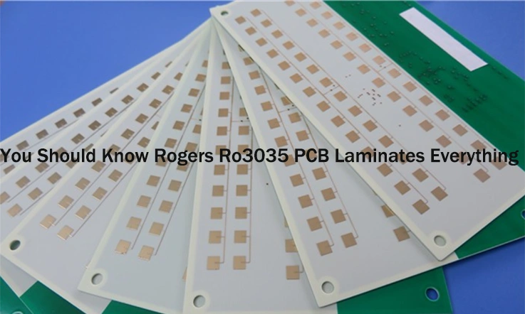
| Material Selection | Built using FR4, polyimide, or high-frequency laminates such as Rogers 4350B. |
| Via Technology | Utilizes blind, buried, and microvias to support dense interconnections. |
| Thermal Considerations | Includes thermal vias, copper coins, and heat-spreading techniques to manage heat effectively. |
| EMI & Signal Integrity | Designed to suppress cross-talk, reflections, and electromagnetic interference. |
| Manufacturing Complexity | Requires precise step-by-step lamination to maintain structural and electrical integrity. |
These boards are built to ensure smooth signal flow, avoiding disruptions that could impact performance in advanced electronic systems.
Where 28 Layer PCB Fits in High-Performance Electronics?
28 Layer PCBs are frequently found in systems that require precise signal integrity and highly compact layouts. Some core applications include:
●Data Centers & AI Servers → Managing large-scale data processing with controlled impedance layouts.
●5G Infrastructure → Supporting high-frequency signal transmission with minimal loss.
●Aerospace & Defense → Used in radar systems, avionics, and satellite communications.
●Medical Imaging Equipment → Ensuring stable signal flow in MRI scanners and diagnostic tools.
For example, 5G base stations rely on stable, high-frequency signals to process vast amounts of data without disruption. If a 28 Layer PCB lacked proper signal integrity, communication speed and system performance would suffer.
Selecting the right materials, layer stack-up, and impedance control methods ensures these boards perform at a consistently high level, even in demanding environments.
Advances in 28 Layer PCB Design & Fabrication Techniques
As electronics continue to shrink in size while increasing in complexity, PCB manufacturing techniques have adapted to keep up with new challenges. Therefore, Now many Engineers and fabricators now use cutting-edge methods to improve efficiency, durability, and overall system integration.
1. High-Performance Substrates & Low-Loss Laminates-
Today many manufacturers have started moving beyond traditional FR4 PCB materials, choosing for substrates like Rogers 4350B, Megtron 6, and Teflon-based composites. These materials offer:
●Lower dielectric loss, ensuring stable, high-speed signal transmission.
●Higher temperature resistance, keeping power-dense circuits from overheating.
●Better mechanical durability, reducing the risk of warping or misalignment during fabrication.
2. AI-Driven PCB Layout Optimization-
Designing a 28 Layer PCB manually can be tedious, and even small routing errors can lead to unexpected performance issues. AI-powered tools now assist in:
●Predicting potential signal bottlenecks and suggesting optimized trace layouts.
●Reducing unnecessary power losses by improving layer distribution.
●Simulating EMI effects, helping designers avoid interference problems before fabrication begins.
3. Hybrid Rigid-Flex & 3D Printed PCB Technology-
The future of 28 Layer PCBs includes hybrid approaches and new manufacturing techniques. Some major advancements include:
●Combining rigid and flexible layers to create compact, lightweight circuit designs.
●3D-printed PCB traces, allowing for rapid prototyping and reduced material waste.
●Embedding passive components directly into PCB layers, saving space and improving reliability.
With these advancements, we can now produce high-density circuit boards that meet evolving performance demands while improving durability.
28 Layer PCB Stack-Up and Advanced Material Selection
When designing a 28 Layer PCB, the stack-up and materials selection is not something that can be taken lightly. The process involves detailed attention to the arrangement of signal, power, and ground layers to avoid interference and ensure that the board performs as expected. The high number of layers in a 28 Layer PCB creates challenges in power delivery, signal integrity, and thermal management. To meet these challenges, advanced materials and a carefully designed stack-up are necessary.
A properly designed stack-up paves the way for reliable signal transmission while minimizing signal degradation, crosstalk, and interference. Thoughtful choices at this stage influence everything from data integrity at high speeds to maintaining thermal efficiency. Nail this step, and you’ve got a PCB ready to tackle demanding performance requirements without a hitch.
Optimizing 28 Layer PCB Stack-Up for Signal Integrity and Power Distribution
Stack-up optimization for a 28 Layer PCB is all about getting the arrangement of the layers correct to ensure that signal integrity and power distribution are balanced. A carefully planned stack-up minimizes the risk of signal degradation, while providing stable power delivery.
Signal Integrity-
To keep signal integrity in check, signal layers should stay near ground planes. This setup helps reduce electromagnetic interference (EMI) and strengthens signal return paths. A well-balanced stack-up supports impedance management, especially in high-frequency designs. The arrangement of ground and power layers influences the reduction of signal noise.
Power Distribution-
In a multi-layer PCB like a 28 Layer PCB, power distribution is a complex task. To ensure that every layer receives stable power, power and ground planes must be placed in a way that allows for efficient current flow while also minimizing voltage drops. This involves strategically positioning power planes next to the layers that need them most.
Here’s an example of a possible optimized stack-up:
| Layer Type | Function | Position |
| Signal Layer 1 | High-speed data routing | Top Layer |
| Ground Plane | EMI shielding & signal return | Layer 2 |
| Power Plane | Power delivery network | Layer 3 |
| Signal Layer 2 | Routing for differential pairs | Layer 4 |
| Ground Plane | Supporting signal integrity | Layer 5 |
| Signal Layer 3 | Routing for high-speed signals | Layer 6 |
| … | … | … |
High-Performance Materials Used in 28 Layer PCB Manufacturing
Selecting appropriate materials for a 28-layer PCB impacts multiple aspects, including signal transmission, heat dissipation, and long-term durability. The chosen materials need to endure the demands of high-frequency operation and repeated temperature fluctuations.
1. Substrate Materials for High-Frequency Performance-
Standard FR4 may suffice for simpler designs, but for a 28 Layer PCB, materials with low dielectric constants and low loss factors are preferred. Materials like Rogers 4350B, Megtron 6, or Teflon offer low signal attenuation, making them suitable for designs that involve high-speed signals.
| Material | Dielectric Constant (Dk) | Dissipation Factor (Df) | Best for Applications |
| FR4 | ~4.3 | ~0.02 | General use PCBs |
| Rogers 4350B | ~3.5 | ~0.0037 | RF & Microwave circuits |
| Megtron 6 | ~3.6 | ~0.002 | High-speed computing circuits |
| Teflon | ~2.1 | ~0.0005 | Aerospace & Military electronics |
2. Copper Thickness Considerations-
The copper thickness impacts current-carrying capacity, heat dissipation, and signal quality. For a 28 Layer PCB, using heavier copper (like 2 oz or 3 oz) in specific layers can provide the necessary power delivery without sacrificing thermal management. When designing power and ground layers, thicker copper allows for improved current handling while reducing resistance.
3. Thermal Management-
In 28 Layer PCBs, heat dissipation is a major factor in ensuring that the board can handle high currents without deforming. Thermal expansion of the materials can also lead to warping or delamination. Materials like ceramic-filled substrates and copper-invar-copper (CIC) cores can be used to manage thermal expansion and keep everything stable.
Copper Thickness and Dielectric Layer Considerations for 28 Layer PCB
In multi-layer PCBs, selecting copper thickness and dielectric materials directly influences signal transmission and overall performance. Copper layers need to support high currents without leading to excessive heat buildup, while dielectric layers should offer sufficient insulation to maintain signal integrity.
1. Choosing the Right Copper Thickness-
For high-frequency applications, copper thicknesses between 1 oz (35 μm) and 3 oz (105 μm) are common. Thicker copper layers are generally used in power delivery systems or high-current circuits, while thinner copper is used for signal routing.
2. Dielectric Material Impact-
The dielectric material separates the copper layers and determines the signal speed. For example, high-performance materials like Rogers RO4000 provide low dielectric loss and stable signal propagation at high frequencies. On the other hand, materials like FR4 are typically used for lower-frequency designs, but they can introduce more signal loss at higher frequencies.
28 Layer PCB Via Technologies for High-Density Interconnects (HDI)
The demand for high-density interconnects (HDI) in modern 28 Layer PCBs continues to grow as electronic devices evolve to meet higher performance expectations. Via technologies enable interlayer connections that ensure stable signal transmission and reliable power distribution. As electronics shrink in size and increase in functionality, the role of vias becomes more pronounced. Understanding how to utilize HDI effectively helps maximize the performance and design efficiency of 28 Layer PCBs.
When designing a 28-layer PCB, the choice of via technology directly impacts electrical performance and structural integrity. Techniques such as microvias and laser drilling enhance connectivity and enable compact, high-density layouts. Let’s dive into the methods that drive advanced interconnect solutions.
Microvias, Blind Vias, and Buried Vias in 28 Layer PCB
In 28 Layer PCBs, the type of vias selected determines how well the layers are interconnected and how efficiently the signals travel across the board. Understanding the distinction between microvias, blind vias, and buried vias helps our engineers choose the most appropriate option for their design requirements.
1. Microvias-
Microvias are small, precise holes, often less than 150 microns in diameter, used for connecting layers in 28 Layer PCBs. These vias are made using laser drilling, allowing for high-density routing with minimal impact on the overall size of the PCB. Microvias are especially effective when a compact design is required, as they help optimize the use of space while ensuring robust electrical connections.
Advantages of Microvias:
●Enable high-density routing without compromising the PCB’s footprint.
●Improve signal integrity in high-speed applications.
●Help reduce the overall size and cost of manufacturing for dense boards.
2. Blind Vias-
Blind vias connect the outer layers of the PCB to one or more internal layers, but they don’t go through the entire thickness of the board. These vias are an excellent choice when you need to connect specific layers without affecting the overall layer stack. Blind vias are particularly useful for high-layer count designs like 28 Layer PCBs, where there is a need to preserve valuable space on the external layers.
Applications of Blind Vias:
●Typically used to link outer layers with inner signal layers.
●Effective in dense PCB designs where space is at a premium.
●Improve routing flexibility without adding complexity to the external layers.
3. Buried Vias-
Buried vias are used to create connections between two inner layers, without reaching the outer layers of the PCB. They are commonly found in multi-layer boards like 28 Layer PCBs, where layer-to-layer communication is needed without interrupting the outer layers. This method optimizes the routing capabilities of the inner layers and minimizes space usage on the external surfaces.
Benefits of Buried Vias:
●Efficiently utilize space in densely packed designs.
●Enhance layer-to-layer communication while maintaining the integrity of the outer layers.
●Simplify the routing process and reduce signal interference in inner layers.
Via-In-Pad and Laser Drilling Techniques for 28 Layer PCB
The via-in-pad technique and laser drilling are integral technologies used in the production of 28 Layer PCBs. These methods allow for precision drilling and optimized interconnections, supporting advanced PCB designs that require small form factors and high performance.
1. Via-In-Pad Technology-
Via-in-pad is a method where vias are placed directly underneath the pads of components. This technique is especially useful when trying to achieve high-density routing and is commonly used in 28 Layer PCBs for components that need to be tightly packed. The use of via-in-pad increases routing capacity without compromising board performance, but it requires special via filling and plating processes to ensure mechanical stability and reliable electrical connections.
Applications of Via-in-Pad:
●Ideal for compact layouts where space is scarce.
●Suitable for high-frequency designs that demand excellent signal integrity.
●Enhances design flexibility by allowing for better routing between layers.
2. Laser Drilling for Precision-
Laser drilling is an advanced technique used for creating small, precise holes in 28 Layer PCBs, especially when dealing with microvias. Laser drilling technology enables the production of vias with very small diameters, which is perfect for high-density designs and is often used in HDI applications. This method provides the precision necessary to meet the requirements of 28 Layer PCBs while maintaining high levels of signal integrity.
Benefits of Laser Drilling:
●Enables precision drilling for smaller vias.
●Perfect for creating microvias that connect high-speed layers.
●Reduces the need for larger, more complex via structures, thus saving space.
Via Filling and Plating Methods to Improve 28 Layer PCB Reliability
Via filling and plating are integral parts of the manufacturing process for 28 Layer PCBs, enhancing both their electrical performance and reliability. These techniques enhance signal integrity and mechanical stability, which are needed for high-density designs.
1. Via Filling Methods-
In via filling, vias are filled with a variety of materials, such as conductive epoxies or non-conductive pastes. This filling process reduces electrical resistance and enhances thermal management by ensuring that heat does not accumulate around the vias. Via filling improves the mechanical strength of the PCB and makes it more resistant to thermal cycling, which is particularly useful for high-performance PCBs.
Via Filling Applications:
●Enhances electrical performance by reducing via resistance.
●Improves thermal dissipation by preventing heat buildup around vias.
●Provides better mechanical support in high-density designs.
2. Via Plating Techniques-
Via plating involves adding metal layers inside the vias to create a conductive path between the layers. Copper is typically used for via plating, as it ensures stable electrical connections. The plating process also enhances the via, improving its durability and resistance to mechanical stress, which is necessary for 28 Layer PCBs that are used in complex applications.
Benefits of Via Plating:
●Provides reliable conductivity between layers.
●Enhances via strength and supports thermal conductivity.
●Creates a smooth surface for efficient component mounting.
Signal Integrity and High-Speed PCB Routing in 28 Layer PCB Design
When designing 28 Layer PCBs, managing signal integrity and ensuring effective high-speed routing are aspects that directly influence the performance and reliability of the final product. As multilayer designs become more complex, signal routing at high speeds must be carefully planned. In 28 Layer PCBs, these considerations are even more pronounced due to the increased number of layers and the demand for fast and reliable signal transmission.
High-speed routing is a fundamental aspect of modern PCB design, particularly for 28 Layer PCBs. We must focus on impedance matching, managing interference, and ensuring the signal can travel through all layers without significant loss. Let’s explore the aspects that go into achieving signal integrity and high-speed performance in 28 Layer PCBs.
Impedance Control and Differential Pair Routing in 28 Layer PCB
In high-speed PCB designs, controlling impedance is a primary factor for ensuring that signals flow through the board without distortion. This is especially true for 28 Layer PCBs, which are commonly required to carry high-frequency signals that can easily be affected by impedance mismatches. Proper impedance control ensures that signals maintain their integrity as they travel through the various layers.
Impedance control ensures that the signal matches the impedance of the transmission line and its load, preventing signal reflection and ensuring the signal reaches its destination without degradation.
Differential Pair Routing-
Differential pair routing is commonly used in 28 Layer PCBs to route two complementary signals. This technique is ideal for high-speed signal transmission, maintaining balance in the signal path and reducing signal loss.
Benefits of Differential Pair Routing:
●Ensures that signals are transmitted with minimal distortion.
●Helps in maintaining synchronized timing between complementary signals.
●Reduces signal degradation by keeping trace lengths equal and tightly controlled.
By ensuring impedance-controlled routing and using differential pairs, 28 Layer PCBs can achieve cleaner signal paths, contributing to enhanced signal quality and improved performance.
Crosstalk and EMI Reduction Techniques for 28 Layer PCB
As the speed of signals in 28 Layer PCBs increases, the risk of crosstalk and electromagnetic interference (EMI) also rises. These issues arise when adjacent signals interfere with each other, leading to data corruption and poor signal transmission.
To manage these concerns, we must apply techniques that minimize crosstalk and EMI, ensuring that high-speed signals remain clean and intact. Optimizing the PCB layout and selecting suitable materials can effectively reduce the chances of signal interference and keep EMI at bay.
Crosstalk Reduction Techniques-
Crosstalk occurs when signals from adjacent traces interfere with each other. In 28 Layer PCBs, where routing density is high, minimizing this interference is a challenge. Some common strategies include:
●Signal Trace Spacing: By increasing the distance between adjacent signal traces, crosstalk can be reduced significantly.
●Shielding: Placing ground planes between signal layers provides an additional shield, absorbing excess electromagnetic radiation.
EMI Reduction Techniques-
Electromagnetic interference (EMI) is a common concern for high-speed circuits, especially when working with 28 Layer PCBs. EMI can disrupt the performance of sensitive components and affect signal quality. To combat this, we can apply:
●Ground and Power Planes: Adding well-defined ground and power planes throughout the PCB helps to contain EMI and minimize its impact on nearby components.
●Via Stitching: Connecting layers with vias at strategic points can help contain EMI and guide the unwanted signals to the ground plane.
High-Speed Signal Transmission Optimization in 28 Layer PCB
To ensure optimal signal transmission, every element of the PCB design must be considered.. Even minor disruptions can affect signal clarity, especially in 28 Layer PCBs that need to support advanced electronics. Optimizing the signal path involves a focus on materials, trace layout, and routing techniques that minimize signal degradation.
Optimizing Signal Path-
The length and complexity of the signal path have a direct effect on transmission quality. In 28 Layer PCBs, we work to minimize trace length and avoid unnecessary bends or obstacles that could interfere with the signal’s path.
●Shortening Trace Length: Shorter paths for signals help minimize signal loss and attenuation, which is particularly beneficial in 28 Layer PCBs that often feature dense routing.
●Layer Stacking: By stacking the layers carefully, it’s possible to keep the signal’s path short, improving its quality as it travels across the board.
Material Considerations-
Selecting the appropriate PCB material influences signal transmission. Materials with low dielectric loss and strong high-frequency properties enable signals to travel more effectively, reducing attenuation and preserving clarity.
●Low-Loss Dielectrics: Materials such as PTFE or ceramic-filled resins are favored for 28 Layer PCBs, as they help reduce signal loss and maintain signal quality even at high speeds.
By focusing on material selection, layer stacking, and trace routing, we can optimize the transmission of high-speed signals in 28 Layer PCBs.
Thermal Management Strategies for 28 Layer PCB Reliability
As the layer count increases in 28 Layer PCBs, managing heat becomes one of the most challenging aspects of the design process. More layers often lead to higher power density, resulting in elevated temperatures. Without proper handling, this heat buildup can lead to component degradation, performance issues, or even failure of the circuit board.
To ensure optimal performance in 28 Layer PCBs under high-performance conditions, effective thermal management techniques are necessary. This includes selecting materials with good thermal conductivity and employing methods to dissipate excess heat from critical areas. The strategies outlined below help manage heat and maintain the PCB’s functionality over time.
Heat Dissipation Techniques for High-Power 28 Layer PCB
Managing heat in 28 Layer PCBs often involves addressing components with high power consumption. Excessive heat in high-power areas can cause components to exceed temperature limits, leading to potential damage. Effective heat dissipation techniques reduce temperature rise, maintaining PCB performance.
Some of the techniques used for heat dissipation include:
| Technique | Description | Effectiveness |
| Heat Sinks | These are attached to components to direct heat away from sensitive areas. | Ideal for areas with high power loads. |
| Thermal Vias | Vias that provide a direct path for heat to travel between layers of the PCB. | Very effective for transferring heat to lower layers. |
| Thermal Pads | Pads placed beneath components to promote heat transfer to the PCB’s layers. | Useful for local heat management. |
| Heat Spreaders | These devices distribute heat over a large surface area to avoid concentrated heat spots. | Helps maintain uniform temperature across the board. |
Example:
In 28 Layer PCBs, heat sinks are often attached to high-power components to prevent overheating. Similarly, thermal vias are used beneath heat-sensitive areas to transfer heat to internal layers where it can be dissipated more evenly. This prevents thermal build-up in one area and ensures a more balanced temperature across the entire board.
Thermal Conductivity Materials Used in 28 Layer PCB
In 28 Layer PCB design, material selection influences heat management efficiency. Materials with high thermal conductivity enhance heat transfer, helping to distribute heat evenly across the PCB. When choosing materials, it’s necessary to consider their thermal properties alongside the electrical and mechanical requirements of the PCB.
The following materials are commonly used for thermal management in 28 Layer PCBs:
| Material | Thermal Conductivity (W/m·K) | Use in 28 Layer PCBs |
| Copper | 398 | Copper is often used in internal copper planes and thermal vias to enhance heat transfer. |
| Aluminum | 235 | Typically used when lightweight but effective heat conduction is necessary. |
| Ceramic-filled Laminates | 0.6-1.4 | Excellent for thermal management where electrical isolation is also required. |
| Thermally Conductive Epoxy | 0.5-1.0 | Used to fill thermal vias and improve heat transfer between layers. |
Material Selection Insight:
●Copper remains the nice material for 28 Layer PCBs due to its ability to efficiently conduct heat. It is widely used for copper planes and thermal vias, especially in high-power or high-density applications.
●Ceramic-filled laminates are suitable when both thermal management and electrical isolation are needed, especially in high-frequency applications.
In addition to these materials, thermally conductive epoxies are often used to fill thermal vias, ensuring optimal heat flow between layers while also maintaining the integrity of the vias.
Role of Thermal Vias and Copper Planes in 28 Layer PCB Cooling
To achieve effective cooling in 28 Layer PCBs, we rely heavily on thermal vias and copper planes. These features facilitate the transfer and distribution of heat across the board, preventing the concentration of heat at specific points.
Thermal Vias-
Thermal vias are drilled holes that connect various layers of the PCB and help move heat from the surface to the lower layers. By conducting heat away from high-power components, they ensure that the temperature does not rise above safe levels.
| Via Type | Description | Application |
| Standard Vias | These vias are typically used to create electrical connections. | Suitable for general-purpose applications. |
| Thermal Vias | Specially designed vias to help move heat between layers. | Excellent for managing temperature in high-power areas. |
| Via-in-Pad | Vias located directly under component pads, helping to conduct heat. | Used under high-power components for effective heat transfer. |
Copper Planes-
Copper planes are used extensively in 28 Layer PCBs to aid in heat dissipation. These continuous copper layers help spread heat from high-power areas, maintaining a steady temperature across the PCB.
| Copper Plane Type | Description | Benefits |
| Ground Plane | Copper layer used primarily for grounding. | Helps distribute heat and ensures grounding stability. |
| Power Plane | Copper layer that distributes power and heat. | Prevents heat buildup in power-dense regions. |
Incorporating both thermal vias and copper planes in 28 Layer PCBs allows us to achieve better heat management, which ensures that 28 Layer PCBs perform efficiently, even in high-power applications.
28 Layer PCB Manufacturing Process and Fabrication Challenges
The process of designing and manufacturing a 28 Layer PCB involves a series of precise steps. These printed circuit boards (PCBs) are commonly used in applications that require high-density and high-performance electronics, such as telecommunications, medical devices, and advanced industrial systems. Each stage in the manufacturing of a 28 Layer PCB presents its own set of challenges, requiring advanced equipment and expertise.
This process includes sequential lamination, fine-line etching, high-precision drilling, and surface finishing. Each of these steps contributes to the final product’s durability and functionality. Let’s explore the specifics of each phase of the 28 Layer PCB manufacturing process.
Sequential Lamination and Layer Bonding in 28 Layer PCB Fabrication
The initial phase in creating a 28 Layer PCB involves bonding multiple layers together using a process known as sequential lamination. The process includes stacking copper foil and dielectric layers, followed by applying heat and pressure to bond the materials.
The Steps:
1.Layer Preparation – Copper foil and dielectric layers are meticulously prepared, ensuring they meet the required size and specifications for the design.
2.Lamination Process – Each layer undergoes a heating and pressure process in a vacuum press to bond the materials. The goal is to eliminate any air gaps between the layers, ensuring stability and electrical integrity.
3.Alignment – The alignment of each layer must be precise to ensure that electrical connections align correctly, particularly for the vias that connect different layers.
| Layer Number | Material Used | Bonding Process | Challenges |
| Layer 1-5 | Copper foil, resin | Initial lamination | Uniform heat distribution |
| Layer 6-12 | High-frequency laminates | Sequential lamination | Preventing warping during heating |
| Layer 13-20 | FR4, prepreg | Bonding under high pressure | Alignment of vias and traces |
| Layer 21-28 | Special composite materials | Final bonding and pressurization | Material deformation control |
Fine-Line Etching and High-Precision Drilling for 28 Layer PCB
After lamination, fine-line etching is used to create the intricate traces and circuitry patterns on the copper layers. Following this, high-precision drilling is performed to create vias and inter-layer connections.
Fine-Line Etching-
This process uses specialized etching chemicals to strip away excess copper, revealing the intended circuit patterns. Precision must be maintained throughout to preserve the integrity of the fine lines and prevent any unintended alterations to the circuitry.
| Etching Method | Feature | Benefit | Challenges |
| Laser Etching | High-precision, small feature sizes | Ideal for complex, multi-layer designs | Managing heat during etching |
| Chemical Etching | Removes excess copper from traces | Effective for large batch productions | Risk of under-etching or over-etching |
| Plasma Etching | Plasma-based technique for fine details | Minimizes distortion of fine traces | Needs cleanroom conditions |
High-Precision Drilling-
High-precision drilling is required to create vias that connect the layers of the 28 Layer PCB. Microvias are often used, which are tiny holes drilled to exact depths to form electrical paths between the layers. The most common drilling techniques are laser drilling and mechanical drilling, both requiring high precision to avoid damage to the PCB.
| Drilling Technique | Features | Application |
| Laser Drilling | Creates fine, precise holes with minimal thermal damage | Used for microvias and via-in-pad |
| Mechanical Drilling | Traditional method using drill bits | Common for larger vias |
| High-Speed Drilling | Extremely fast and precise process | Ideal for high-volume production |
Surface Finishing and Solder Mask Application in 28 Layer PCB Production
Once the etching and drilling processes are complete, surface finishing is applied to ensure the copper is protected and ready for component placement. The application of solder mask ensures that there are no unintended solder bridges between traces and pads.
Surface Finishing-
The surface finishing process involves applying coatings to the PCB’s copper surfaces. This provides a smooth and durable layer that protects the copper from corrosion and wear. Several finishing techniques are available, including HASL (Hot Air Solder Leveling) and electroplated finishes. These ensure the PCB is suitable for long-term use.
| Finishing Type | Description | Benefits |
| HASL (Hot Air Solder Leveling) | A hot air process to apply a thin solder layer over copper pads | Provides smooth, uniform coating |
| Electroplating | Electrolytic process to coat copper surfaces with a solderable finish | Highly durable and corrosion-resistant |
| ENIG (Electroless Nickel Immersion Gold) | Coats the copper with nickel and gold | Ideal for high-frequency applications |
Solder Mask Application-
Once the surface finishing is complete, a solder mask is applied to prevent any accidental connections during component soldering. The solder mask also provides protection against environmental factors that might degrade the PCB over time. Commonly, green solder mask is used, although other colors can also be selected based on design needs.
| Solder Mask Type | Feature | Benefits | Challenges |
| Photoimageable Solder Mask | Allows for intricate patterning | Perfect for high-density designs | Needs precise application |
| Epoxy-based Solder Mask | Strong adhesion, heat resistance | Ideal for high-temperature applications | Requires careful curing process |
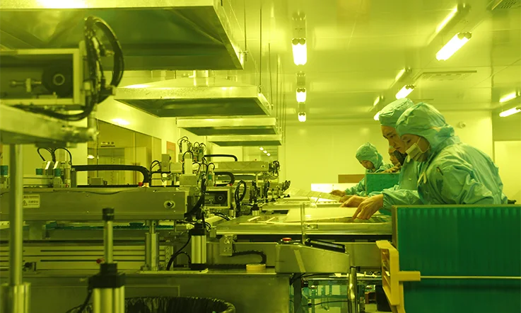
PCB Assembly and Soldering Techniques for 28 Layer PCB
When it comes to 28 Layer PCBs, the assembly and soldering process is a defining factor in ensuring that these high-density circuits work effectively and reliably. As the demand for smaller, more powerful devices increases, the complexity of the assembly process also escalates. In this section, we’ll dive deep into the nuances of SMT (Surface Mount Technology) and Through-Hole Assembly, as well as explore the latest automated pick-and-place technologies. Additionally, we’ll discuss the soldering challenges that come with such a multi-layered PCB and how to optimize the reflow profile to ensure top-notch performance.
The assembly of 28 Layer PCBs requires a careful balance of precision, technology, and process management. This balance is needed to address the unique challenges of layer bonding, high-density interconnects (HDI), and precise component placement. Let’s get into the nitty-gritty of these techniques.
SMT vs. Through-Hole Assembly for 28 Layer PCB Manufacturing
SMT (Surface Mount Technology) and Through-Hole Assembly are the two primary methods used for placing components on a 28 Layer PCB. While both have their own advantages and challenges, the choice of method largely depends on the design of the board and the specific requirements of the end product.
SMT Assembly-
Surface Mount Technology is the go-to for high-density and compact designs like 28 Layer PCBs. SMT components are mounted directly onto the surface of the PCB, and the process is automated for high precision. The main advantage of SMT is that it allows for a more compact design, as it eliminates the need for holes in the PCB, allowing components to sit flat against the surface.
Benefits:
●Faster production time due to automated assembly.
●Reduced board size, fitting more components in a smaller area.
●Improved signal integrity with fewer vias and less complicated routing.
| Component | SMT Advantage | Challenge |
| Resistors | Smaller size, more placements | Can be difficult to repair |
| Capacitors | Easier placement, quicker | Limited to smaller components |
| ICs | Efficient for high-density | Higher cost for complex designs |
Through-Hole Assembly-
Through-hole assembly, while not as commonly used in modern high-density boards, can still be required for certain components that need strong mechanical connections, such as connectors and larger capacitors. This method involves drilling holes through the PCB and inserting components into these holes, which are then soldered on the other side.
Benefits:
●Stronger mechanical connections for high-stress applications.
●Better for larger components that require more support.
| Component | Through-Hole Advantage | Challenge |
| Connectors | Strong mechanical support | More space required on the board |
| Power ICs | Stable for high power | Takes up more space |
Automated Pick-and-Place Equipment for 28 Layer PCB Assembly
In 28 Layer PCB assembly, automated pick-and-place equipment has enhanced the efficiency and accuracy of component placement. This technology enables the rapid positioning of thousands of components with precise alignment, which is especially beneficial for high-density circuit boards.
How It Works-
Automated pick-and-place machines work by using robotic arms to pick up components from reels or trays and place them precisely on the PCB. These machines use vision systems to check the alignment of the components, ensuring each one is placed exactly where it should be.
Benefits:
●Precision – The vision system ensures perfect alignment.
●Efficiency – Reduces manual labor and speeds up production time.
●Flexibility – Capable of handling both small and large components with ease.
| Machine Type | Features | Application |
| Standard Pick-and-Place | Simple and effective for most components | Used in high-volume production |
| Advanced Vision Systems | Precision component placement | Ideal for complex, high-density boards |
| Customized Robotic Arms | Can handle unique, large components | Useful for specific high-power components |
Soldering Challenges and Reflow Profile Optimization for 28 Layer PCB
Soldering is a first step in the assembly process of 28 Layer PCBs. Reflow soldering is typically used for SMT components, while wave soldering may still be employed for through-hole components. However, given the multiple layers and complexity of the 28 Layer PCB, optimizing the reflow profile becomes an art.
Soldering Challenges-
The primary challenge in 28 Layer PCB soldering is heat management. With so many layers, excess heat can cause warping or thermal stress, which can damage the PCB or components. Additionally, because the traces and vias are often densely packed, achieving uniform soldering can be tricky.
Reflow Profile Optimization-
Optimizing the reflow profile ensures that the temperature increases at the right rate to melt the solder without damaging the board. This involves controlling the heating, soaking, and cooling stages of the reflow process.
| Phase | Temperature Range | Purpose |
| Preheat | 150-180°C | Gradual heating to avoid thermal shock |
| Soak | 180-220°C | Allows flux activation and temperature stabilization |
| Reflow | 220-250°C | Melts solder to connect components |
| Cooling | 25-40°C/minute | Cool down to solidify solder connections |
Benefits of Optimizing the Profile:
●Prevents thermal stress on the PCB.
●Minimizes solder defects like tombstoning and bridging.
●Increases yield rate by ensuring consistent solder joints.
Quality Control, Testing, and Reliability Standards for 28 Layer PCB
A 28-layer PCB is far from an ordinary circuit board. The complexity of such multilayer designs requires not only precise manufacturing but also rigorous testing protocols to prevent electrical failures, mechanical stress issues, and long-term degradation. To maintain flawless performance across industries like aerospace, telecommunications, and high-speed computing, manufacturers adhere to well-defined industry standards and implement cutting-edge inspection techniques.
From IPC certifications ensuring compliance to automated optical and X-ray inspections detecting hidden defects, and environmental stress testing simulating real-world conditions, each step plays a role in guaranteeing rock-solid reliability. Let’s explore the stringent measures in place that keep 28-layer PCBs performing at their peak.
IPC Standards and Industry Certifications for 28 Layer PCB
A 28-layer PCB must conform to strict industry regulations to guarantee reliability, electrical performance, and safety. Organizations such as IPC (Association Connecting Electronics Industries) set the standard for PCB manufacturing, ensuring that materials, fabrication processes, and end-product quality meet defined benchmarks.
Key IPC Standards for 28 Layer PCBs-
●IPC-6012: Covers qualification and performance standards for rigid PCBs, addressing material specifications, conductor integrity, and dielectric properties.
●IPC-A-600: Defines acceptable PCB appearance, ensuring the board is free from defects such as voids, delamination, or misalignment.
●IPC-2221: Governs the general design principles for electronic interconnects, including layer stacking, trace routing, and via structures.
Alongside IPC certifications, manufacturers often pursue UL (Underwriters Laboratories) certification, which verifies that PCB materials meet flammability and insulation safety requirements. Additionally, ISO 9001 certification helps standardize quality management processes, reducing manufacturing defects and improving overall product consistency.
For main applications such as medical devices or aerospace electronics, PCBs must also comply with AS9100 and MIL-PRF-31032 standards, which set higher reliability and traceability requirements.
AOI, X-ray Inspection, and Functional Testing for 28 Layer PCB
With 28-layer PCBs, defects aren’t always visible to the naked eye. Complex stacking, fine-pitch components, and dense routing demand advanced inspection methods to catch potential issues before assembly is complete.
Inspection Techniques for 28 Layer PCBs-
1.Automated Optical Inspection (AOI) – Using high-resolution cameras and machine-learning algorithms, AOI systems quickly scan PCB surfaces for solder joint issues, missing components, and trace breaks. This method is effective for detecting visible flaws in surface-mount components and outer layers.
2.X-ray Inspection – Unlike AOI, X-ray testing can penetrate the PCB’s layers, allowing us to examine buried vias, solder balls under BGAs, and internal defects. This is especially useful in HDI (High-Density Interconnect) designs, where traditional inspection methods fall short.
3.Functional Testing – After assembly, real-world electrical loads and signals are applied to confirm that all circuits behave as expected. Functional tests simulate actual working conditions, ensuring the PCB can handle its designated workload without errors.
By integrating AOI, X-ray, and functional testing, we can eliminate defects early, preventing costly failures and reducing unnecessary rework.
Reliability Testing: Thermal Cycling, Vibration, and Aging for 28 Layer PCB
A 28-layer PCB must endure intense environmental conditions without performance degradation. Whether exposed to temperature fluctuations, mechanical stress, or long-term high-power loads, reliability testing ensures the PCB can handle its intended application.
Common Reliability Tests for 28 Layer PCBs-
1.Thermal Cycling – Simulates extreme temperature swings to check for material expansion/contraction issues. PCBs used in automotive, aerospace, and industrial applications may be tested from -55°C to 125°C over hundreds of cycles to mimic real-world conditions.
2.Vibration Testing – Applies mechanical stress to assess structural integrity. This is essential for satellites, drones, and electric vehicles, where constant vibrations can weaken solder joints and cause component failure.
3.Aging and Humidity Tests – Prolonged exposure to 85°C and 85% humidity for 1,000+ hours mimics years of wear and tear, helping us identify potential long-term failure points before mass production.
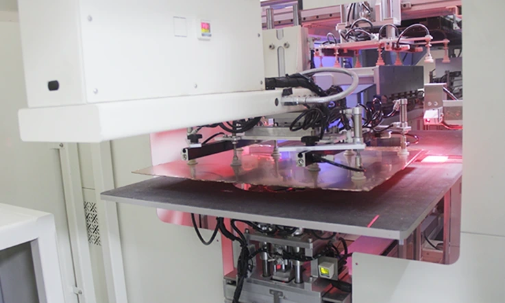
PCB Fabrication
Multilayer PCB Manufacturing & Assembly