A PCB trace, also referred to as a PCB track, is a narrow copper conductor found on the surface of a printed circuit board that is responsible for carrying electrical signals. These traces are created through the process of selectively etching away the surrounding copper foil, resulting in a flat and slim pathway. Printed Circuit Boards serve as the fundamental building blocks of contemporary electronic devices, playing a pivotal role in connecting and supporting diverse electronic components.
Designing a PCB obliges a careful contemplation of numerous factors, which the selection of copper weight is paramount since it dictates the thickness of the copper layer inscribed on the board. In this article, we will delve into the universe of 2 oz Copper PCB with an emphasis on their merits, use-cases, the intricate fabrication procedures, and the driving forces behind their surging popularity in the realm of electronics.
What is A 2 Oz Copper PCB?
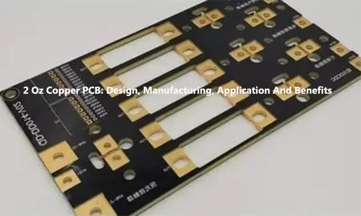
A 2 oz copper PCB is characterized as a type of printed circuit board that features a copper weight of two ounces per square foot. It possesses a standard internal copper layer with a uniform metal thickness. Additionally, it incorporates a 3 oz finished copper layer for improved arrangement of the external layers.
The production of a 2 oz copper PCB entails the use of around two ounces of superior grade copper to meet the desired dimensions. This copper is uniformly distributed over the PCB, spanning an area equal to one square foot. Thus, the attained thickness of the 2 oz copper circuit equates to roughly 2.8 mils or 70 micrometers.
This type of PCB, known for its efficiency in prototypes, is widely used in circuit boards. Its thickness provides ample benefits as the primary foil in various electronic appliances. Furthermore, the 2 oz copper PCB surpasses the 1 oz copper PCB in terms of compatibility with etched boards, making it a superior choice.
Overall, due to its particular copper weight and thickness, the 2 oz copper PCB is highly regarded and finds extensive application within the field of printed circuit boards.
Properties of 2 Oz Copper PCB
The thickness of the copper layer on a PCB can be deduced from the unique characteristics it endows. For the case of a 2 oz copper PCB, one can witness the subsequent properties:
Copper Weight: The PCB features a copper weight of 2 ounces per square foot, indicating a relatively thick copper layer for improved current carrying capacity.
Panel Size: The dimensions of the PCB panel measure 2 feet by 2 and a ½ feet, defining the overall size of the board.
Minimum Copper Traces: The PCB supports minimum copper traces of 7 mils, allowing for finer and more intricate circuitry designs.
Hole Diameter: The PCB incorporates holes with a minimum diameter of 0.15 mm, facilitating the placement of components and providing necessary connectivity.
Material Composition: The thickness of the copper in the PCB can vary depending on the specific material composition used. The chosen materials contribute to achieving the desired copper thickness.
Impedance Control: The PCB offers excellent impedance control, enabling precise management of signal integrity and impedance matching requirements.
Liquid Photo-Imageable Mask: The PCB utilizes a liquid photo-imageable mask, a technique commonly used in PCB manufacturing for precise layer alignment and protection during etching processes.
Multilayer Vias: The PCB provides vias for multilayer boards, allowing for reliable interconnection between different layers and facilitating complex circuit design.
These properties collectively contribute to the functionality, reliability, and design considerations of a 2 oz copper PCB, making it suitable for various applications in the field of electronic engineering.
Benefits of 2 Oz Copper PCB
One of the primary advantages of utilizing 2 oz Copper PCB lies in their enhanced current-carrying capacity, which stems from the thicker copper layer. This attribute significantly reduces resistance and facilitates the smooth flow of higher current levels, making these PCB particularly well-suited for power electronics and applications demanding robust electrical performance. The minimization of resistive losses allows for more efficient power transfer while mitigating the risk of component overheating.
A significant perk that 2 oz Copper PCB introduces is superior thermal management. The augmented copper weight amplifies the PCB’s proficiency at disseminating heat optimally. Known for its extraordinary thermal conduction traits, copper ensures effectual propagation and dispersion of heat produced by power components. Hence, 2 oz Copper PCB surface as immensely beneficial for gadgets functioning under high-power or high-temperature conditions. The heightened thermal management abilities furnished by these PCB are pivotal in assuring the dependability and lifespan of the components.
In addition, 2 oz Copper PCB offer enhanced durability and reliability thanks to their thicker copper layer. This feature contributes to amplified mechanical strength, making them less prone to tension-induced distortions like warping and bending. Additionally, the heightened copper weight bolsters the PCB’s resilience against environmental elements like humidity and corrosion, bestowing extended dependability on the circuitry. Such attributes render 2 oz Copper PCB supremely ideal for critical applications across sectors like aerospace, industrial, and automotive.
Moreover, the increased copper weight in 2 oz PCB contributes to lower impedance and reduced signal loss. This characteristic is crucial in high-frequency applications where maintaining precise impedance throughout the circuit is essential for accurate signal transmission. By offering lower impedance, 2 oz Copper PCB exhibit reduced signal loss, leading to improved signal integrity and diminished distortion. Consequently, these PCB find widespread use in applications involving RF (Radio Frequency), microwave, and high-speed digital circuits.
By capitalizing on the advantages of 2 oz Copper PCB, engineers and PCB designers can effectively optimize their designs to accommodate higher current requirements, ensure efficient thermal management, enhance durability, and maintain excellent signal quality in a diverse range of electronic applications.
Key Considerations for 2 oz PCB Current Carrying Capacity
The current carrying capacity of a circuit board to conduct electricity are shaped by several determinants, elaborated as follows:
Trace Cross-Sectional Area: The size of the traces sectional area is crucial, for determining how much current the circuit board can handle. Increasing this area enables higher current to flow through the PCB.
Copper Thickness: The thickness of the copper in a 2 oz PCB directly affects its ability to conduct current. The capacity to carry electricity is contingent on the copper volume present on the board. Hence, a boost in copper thickness simultaneously escalates the PCB’s current carrying capability as well.
Temperature: Temperature is another crucial factor that impacts the current carrying capacity of a 2 oz copper board. The operational environment of the PCB influences the current flow. Lower temperatures generally result in increased current conduction in the PCB.
How to Calculate 2 Oz Copper PCB Thickness?
For calculate the thickness of a 2 oz copper PCB, it is pivotal to comprehend the copper weight measurement system deployed in PCB production. The copper weight is gauged in ounces per square foot (oz/ft²) and signifies the copper layer’s weight on a one-square-foot zone of the PCB.
Copper Thickness (in mils) = (Copper Weight in oz/ft²) / (1.37 * Copper Density).In this formula, the copper density is typically taken as 1.4 g/cm³ for standard copper used in PCB.
To convert the result to a more commonly used measurement, like micrometers (um) or mils (thousandths of an inch), the subsequent conversions can be employed:
●1 mil = 25.4 micrometers (um)
●1 mil = 0.001 inch
●Here’s an example calculation:
●Copper Thickness (in mils) = (2 oz/ft²) / (1.37 * 1.4 g/cm³)
●Copper Thickness (in mils) = 1.45 mils
1 Oz vs. 2 Oz Copper PCB
While contrasting 2oz copper PCB with 1oz counterparts, a handful of distinguished differences emerge. Primarily, 2oz copper PCB boast superior power management capabilities, rendering them more compatible with adapters and chargers. They are proficient in reliably conducting higher currents compared to 1oz copper PCB.
In terms of efficacy, 2 oz copper PCB weigh more than 1 oz copper PCB, providing enhanced thermal control. This makes them well-suited for applications where effective heat dissipation is crucial.
2 oz copper PCB find broader applications in areas that demand high power transmission compared to 1 oz copper PCB. They are particularly advantageous for handmade prototypes as they allow for easy peeling of the area. On the other hand, 1 oz copper PCB offer greater soldering convenience.
Regarding thickness, 2 oz copper PCB contain two ounces of copper, while 1 oz copper PCB have one ounce of copper. This difference in copper weight necessitates different manufacturing processes for each type.
It’s important to note that choosing 2 oz copper PCB over 1 oz copper PCB often entails higher operational and maintenance costs due to the increased copper weight and related manufacturing requirements. As such, these factors should be considered when making decisions for specific PCB projects.
Design Guidelines for 2oz Copper Boards
To fully optimize a design utilizing 2oz copper thickness, PCB engineers should adhere to specific layout guidelines:
Utilize Available Space: Leverage the advantages of narrower traces and spacing offered by 2oz copper to achieve denser component placement. Strategically spread out components to make efficient use of the extra space.
Minimize Trace Lengths: The reduced resistivity of 2oz copper decreases the need for wide traces. Make optimal use of the additional space to create shorter and more direct connections.
Reduce Layer Count: The lower current density supported by 2oz copper may allow for the elimination of unnecessary layers, if feasible within the design. However, ensure that sufficient ground and power planes are maintained.
Use Smaller Vias: Leverage the finer resolution of 2oz copper to shrink via sizes while preserving routing density, optimizing space utilization.
Increase Component Density: Take advantage of thinner 2oz traces to facilitate interconnections between smaller package components, enabling higher component density within the design.
Address AC Impedance: Pay close attention to high-frequency signals and ensure that narrow 2oz traces are kept short while avoiding the use of thin and long traces to maintain proper AC impedance.
Eliminate Thermal Reliefs: If suitable for components and leads, consider eliminating thermal reliefs to reduce thermal resistance, thereby enhancing thermal management within the design.
Enhance Copper Fills: Utilize additional copper pours to improve thermal dissipation and provide EMI shielding, while ensuring proper isolation from traces.
Reduce Plane Splits: Minimize the number of splits in ground and power planes to maintain integrity. Use additional vias to establish connections through plane splits when necessary.
Watch Spacing at Edges: Be mindful of spacing requirements along the board edges, as the higher etch resolution of 2oz copper may result in insufficiently spaced traces.
Refine Grids/DRC Rules: Adjust clearance grids and design rule checks to align with the capabilities offered by 2oz copper, ensuring optimal design integrity.
Account for Via-in-Pad: Consider via-in-pad rules, particularly when densely placing vias, to ensure proper functionality and reliability.
By following these meticulous PCB layout guidelines for 2oz copper, engineers can potentially reduce board sizes, maximize performance, and minimize overall assembly costs, resulting in an optimized design.
Manufacturing Process Of 2 Oz Copper PCB
Fabricating a 2 oz copper PCB is a meticulous and intricate process due to the heavy copper weight involved. However, by adhering to these crucial steps, manufacturers can simplify and ensure the success of the fabrication process.
Preparation:
The initial step entails meticulous preparation of the materials necessary for fabricating the 2 oz copper PCB. Computer programs can be utilized to aid in the preparation, offering predefined instructions and guidance.
Plotting:
A photo plotter machine plays a vital role in achieving accurate designs for the prepared materials. This machine creates precise patterns on the 2 oz copper board based on the specific requirements of the application. The manufacturer designs and configures the thin inner layers accordingly.
Lamination:
During the lamination process, the internal layers of the PCB are subjected to high pressure. This pressure assists in firmly bonding the layers together. Manufacturers employ a photosensitive dry resist for lamination, ensuring optimal adhesion and integrity.
Component Placement:
Drilling holes on the PCB is an essential phase of component placement. The manufacturer employs precise drilling techniques and subsequently plates the drilled holes to enhance the conductivity of electrical currents.
Solder Masking:
To protect the copper traces and facilitate soldering, a solder mask is applied to coat the PCB surface. This masking process ensures proper insulation and prevents undesired solder bridges or shorts. Additionally, a suitable surface finish is applied to the PCB, enhancing solderability and preventing oxidation.
Testing:
To validate the functionality of the 2 oz copper PCB, rigorous testing and inspection are performed. This step ensures that the PCB meets the required electrical specifications and design parameters, guaranteeing its reliability and performance.
By following these fundamental steps, PCB manufacturers can successfully fabricate 2 oz copper PCB, meeting the demands of high current applications with precision and effectiveness.
Applications that Benefit from 2oz Copper
Several types of PCB designs and applications can significantly benefit from the superior performance offered by 2 oz copper. These applications leverage the enhanced capabilities of 2 oz copper to meet their specific requirements and ensure optimal performance and reliability.
High Power Electronics:
Applications such as HVAC systems, motor drives, battery charging, power supplies, and other high-power devices necessitate robust PCB capable of handling substantial currents without the risk of overheating. By employing 2 oz copper PCB, these applications can effectively manage the demanding power requirements while minimizing resistive losses.
Automotive Electronics:
Under-hood circuits for engines, drivetrains, and auxiliary systems in the automotive sector demand highly reliable PCB that can withstand the extreme thermal and vibration conditions. By utilizing 2oz copper PCB, automotive electronics benefit from improved thermal management and mechanical strength, ensuring reliable operation in harsh environments.
LED Lighting:
High-luminosity LED lighting systems frequently function at escalated temperatures, potentially impacting the LEDs’ efficiency and lifespan along with their drivers. Through incorporating of a 2oz copper PCB, these lighting systems can proficiently dispel heat and sustain optimal operational temperatures, thereby boosting the efficacy of light output.
Power Amplifiers:
Audio amplifiers and transmitters dealing with large RF signals require PCB with low loss characteristics to ensure clean signal amplification. By utilizing 2 oz copper, power amplifiers can minimize signal loss and achieve optimal performance, particularly in high-frequency applications.
Computer Servers:
High-density computing clusters in server applications require densely populated PCB to interconnect numerous processors operating at high power levels. The use of 2 oz copper PCB allows for efficient power distribution and heat dissipation in these densely packed server systems.
Wireless Base Stations:
Wireless base stations handling multiple simultaneous cellular signals generate substantial heat within their crowded enclosures. By utilizing 2 oz copper PCB, these base stations can efficiently dissipate heat, ensuring reliable operation and prolonged lifespan of the critical wireless infrastructure.
Defense/Avionics:
Aerospace systems, particularly those categorized as mission-critical in defense and avionics applications, demand maximum reliability even under demanding operating conditions. By employing 2oz copper PCB, defense and avionics systems can achieve the required level of reliability and performance in challenging thermal and electrical environments.
Medical:
Implantable medical devices like pacemakers and monitors require robust PCB that can withstand thermal stresses and accommodate high currents within the body. With 2 oz copper PCB, these medical devices ensure robust operation and longevity, improving overall performance and patient safety.
The adoption of 2oz copper PCB over the 1oz type, despite a minor uptick in manufacturing costs, is favoured in these specific use-cases owing to its significant benefits. The perks of augmented current capacity, superior thermal management, and bolstered reliability render 2oz copper PCB the optimal selection for these intricate and demanding applications.
Conclusion
Due to the increasingly demanding performance requirements of modern electronics, the adoption of 2oz copper PCB has been gaining prominence over conventional 1oz constituents across a multitude of applications. This preference stems from substantial advantages such as enhanced electrical performance, superior thermal management, improved reliability, and expanded fabrication capabilities.
To fully exploit the advantages of lower losses, higher current capabilities, improved resolution, and enhanced shielding provided by 2oz copper, designers must adopt disciplined layout practices tailored specifically for the unique characteristics of thicker copper boards.
By pairing robust 2oz PCB technology with optimized design techniques, engineers can effectively construct electronic products that offer maximized efficiency, density, and reliability, thereby catering to the evolving needs of the future.

