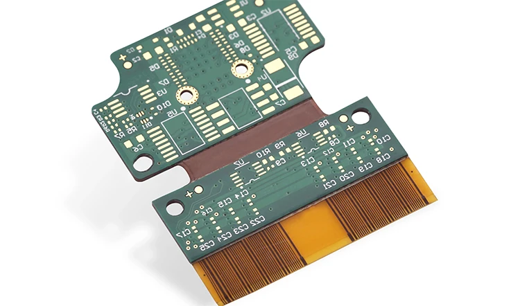
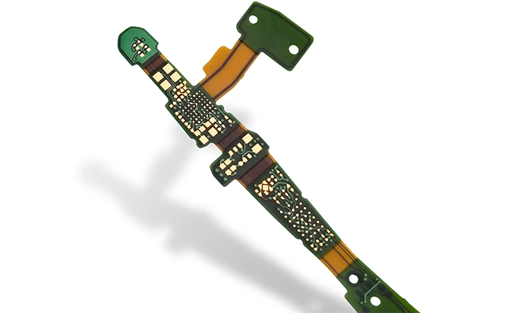
18-layer rigid-flex PCBs are becoming increasingly integral to a variety of high-tech industries due to their unique design capabilities and extensive applications. From wearable electronics to medical devices and aerospace technologies, these circuit boards require a high level of precision and balance between size, functionality, and durability.
In this article, we will delve into the design principles, manufacturing, and assembly processes of 18-layer rigid-flex PCBs. Additionally, we will explore how different industries influence PCB layer design and manufacturing workflows, providing insights on how to optimize these circuit boards for complex technological demands. Whether you are seeking solutions for next-generation wearable devices or meeting the specialized requirements of medical and aerospace sectors, this guide will offer valuable knowledge and practical advice to enhance your design and manufacturing approach.
What is 18 Layer Rigid-Flex PCB and Why Choose It?
The 18-layer rigid-flex PCB offers an innovative design combining rigid and flexible layers, making it a preferred option for applications requiring compact, high-performance circuits. This type of PCB offers unique advantages in sectors where space is constrained, and reliable performance is required under different conditions.
Key Features of 18 Layer Rigid-Flex PCB
Let’s break down the standout characteristics of the 18-layer rigid-flex PCB that make it a versatile option in various industries:
1.Dual Nature-
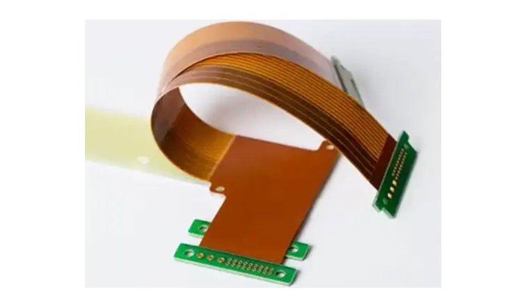
The 18-layer rigid-flex PCB incorporates both rigid and flexible materials. Rigid sections typically use FR4, while flexible parts often employ materials like polyimide. This allows the board to take on the best features of both, offering structural stability in certain areas while allowing flexibility in others.
2.Layer Structure for Better Performance-
The multi-layer design of the 18-layer rigid-flex PCB helps optimize both thermal management and signal integrity. Multiple copper layers within the stack-up assist in efficiently distributing heat, making it easier to handle temperature-sensitive components, particularly in high-power applications.
3.Efficient Space Utilization-
The flexible sections of the board allow for better space management. This design is especially useful in applications where compact form factors are necessary, such as wearables, medical devices, or consumer electronics. This type of PCB can fit into small, confined spaces while still providing high performance and functional diversity.
4.Effective Heat Dissipation-
The 18-layer rigid-flex PCB efficiently disperses heat across the board, reducing the risk of overheating and ensuring that electronic components perform at optimal levels, even in high-temperature environments.
Example:
For a smartwatch, the 18-layer rigid-flex PCB can house both a flexible display and a rigid processing unit in a compact form factor. The rigid-flex design ensures reliable signal transmission and battery performance, all while maintaining a lightweight, comfortable fit.
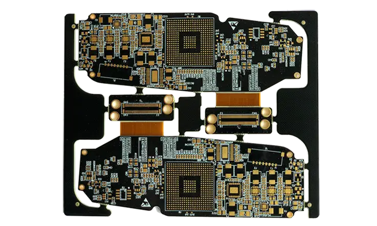
18-Layer Rigid-Flex PCB vs. Traditional Multilayer PCBs
When comparing the 18-layer rigid-flex PCB to traditional multilayer PCBs, there are a few important differences to consider:
1.Signal Integrity-
Traditional multilayer PCBs often face challenges when dealing with longer signal paths or high-frequency transmissions. The 18-layer rigid-flex PCB, however, minimizes signal degradation by allowing shorter, more direct signal routing, improving signal clarity and transmission speeds. The flexibility of the design also helps reduce the chance of issues like cross-talk or interference.
2.Thermal Management-
The 18-layer rigid-flex PCB excels at thermal control, helping to evenly distribute heat and prevent overheating in high-power applications. Traditional multilayer PCBs often struggle with efficient thermal dissipation, particularly in dense, high-performance circuits, which can result in higher temperatures that may impact the board’s performance and lifespan.
3.Design Flexibility-
While traditional rigid PCBs offer stability, the 18-layer rigid-flex PCB provides the advantage of flexibility. This flexibility allows the board to be shaped or conformed to fit into irregular spaces, making it suitable for devices like wearables that require precise fit and placement. The flexibility also makes these boards suitable for dynamic applications where the board might experience movement or shifting.
4.Durability and Longevity-
The 18-layer rigid-flex PCB is designed to withstand physical stresses such as vibrations, impacts, and temperature fluctuations, which are common in industries like aerospace and automotive. Multilayer PCBs may not be as durable under these conditions, potentially leading to performance issues or failures.
Example:
Consider an aerospace satellite that uses an 18-layer rigid-flex PCB. The flexible design ensures that the PCB can endure the physical stresses of launch and operate reliably in the harsh environment of space, where traditional rigid PCBs might face issues due to high vibrations or thermal extremes.
Applications of 18 Layer Rigid-Flex PCB in Cutting-Edge Industries
The 18-layer rigid-flex PCB is becoming more common in a variety of innovative sectors, especially in devices and systems where compactness, functionality, and long-lasting performance are needed. Below are some industries where rigid-flex PCBs are making a difference:
1.Wearable Electronics-
Devices like smartwatches and fitness trackers require high-density circuits in a small footprint. The 18-layer rigid-flex PCB fits this need perfectly, enabling us to pack powerful, multi-functional systems into a compact space. The flexible nature of the PCB also ensures comfort and wearability, with no compromise on performance.
2.Medical Devices-
Medical devices, including implantable systems like pacemakers, need to be both small and highly reliable. The 18-layer rigid-flex PCB allows for the creation of small yet powerful systems that can operate continuously within the body. Its flexibility also helps reduce the stress on the components, ensuring consistent operation over time, even in dynamic environments like the human body.
3.Aerospace-
In aerospace, where equipment must withstand extreme conditions such as high levels of vibration and temperature extremes, the 18-layer rigid-flex PCB is best. Its ability to handle these conditions while maintaining signal integrity and performance makes it an reliable choice for satellite electronics, navigation systems, and other critical aerospace applications.
4.Consumer Electronics-
In the consumer electronics sector, products like smartphones and VR headsets often require compact yet high-performing components. 18-layer rigid-flex PCBs offer the perfect balance, allowing for the inclusion of multiple high-density circuits without taking up extra space. The flexibility of these boards also aids in space optimization, particularly in devices that require unique form factors or curved surfaces.
What Did You do Before Design a 18 Layer Rigid-flex PCB?
Before diving into the design of an 18-layer rigid-flex PCB, a series of essential steps can help ensure the final product meets performance and manufacturing needs.
1.Optimize Layer Stack-Up: Consider how layer organization impacts electrical performance, signal integrity, and impedance control. A well-balanced stack-up helps minimize issues during operation.
2.Material Selection: Choose rigid and flexible materials based on their thermal, mechanical, and production characteristics. Flex materials like polyimide work well for areas requiring bending, while rigid materials provide the structural strength needed for complex components.
3.Signal Integrity Considerations: Incorporate impedance-controlled routing and perform thorough signal integrity analysis (SI). This ensures high-frequency signals flow correctly, preventing delays or signal loss.
4.Define Flex Bend Radius and Transition Zones: Carefully plan for bending areas, specifying minimum bend radii and transition zones to prevent damage during use. Flexibility should not hinder the performance of the circuits.
5.Thermal Management: Implement strategies such as thermal vias and heat sinks to manage temperature rise. Proper thermal dissipation keeps the PCB working efficiently even in high-performance applications.
6.Efficient Component Placement: Minimize potential problems like crosstalk and electromagnetic interference (EMI) by positioning components thoughtfully. Route traces in a way that avoids long, inductive paths, especially for high-speed signals.
7.Power Distribution Design: Plan for proper power delivery with enough current capacity, balancing power planes and vias to ensure a stable, noise-free power supply.
8.Account for Manufacturing Constraints: Recognize the limitations of your PCB manufacturer. Avoid overly tight tolerances or complex designs that might drive up costs or complicate production.
9.Easy Assembly and Interconnections: Keep the design straightforward for assembly. Including test points or using accessible vias can ease the process when assembling the board and troubleshooting.
10.Test for Reliability: Ensure the design is robust under conditions like mechanical stress, temperature cycles, and vibration, particularly for products that will face harsh environments.
11.Validation and Testing: Confirm the functionality, performance, and reliability of the design with thorough testing. This helps pinpoint any issues before mass production.
12.Standards Compliance: Ensure the design complies with industry standards such as IPC, UL, RoHS, ISO, and any specific regulations in the product’s application area. Adhering to these standards ensures quality control and smooth certification processes.
Design Considerations for 18 Layer Rigid-Flex PCB
Designing a 18-layer rigid-flex PCB involves several considerations to ensure the board meets performance and reliability requirements. Below are the core considerations when designing an 18-layer rigid-flex PCB, from material selection to signal integrity and stack-up optimization.
Importance of Material Selection for 18 Layer Rigid-Flex PCB
Selecting the appropriate materials for an 18-layer rigid-flex PCB can have a significant impact on the board’s overall performance and reliability. Materials should be chosen based on application needs such as flexibility, thermal resistance, and signal integrity. Below is a breakdown of the material options commonly used in rigid-flex PCB designs.
| Material Type | Properties | Applications |
| Flexible Substrates | High flexibility, excellent thermal resistance | Wearables, medical devices, and aerospace applications |
| Rigid Laminates | Structural support, excellent mechanical properties | Complex components, supporting high-density circuits |
| Thermal Management Materials | High thermal conductivity, EMI shielding | Medical devices, aerospace, high-performance electronics |
1.Flexible Substrates-
For the flexible sections of the 18-layer rigid-flex PCB, materials such as polyimide or PPE are often used due to their excellent flexibility and thermal resistance. These materials can endure bending without compromising integrity, making them suitable for wearables and implantable medical devices.
2.Rigid Laminates-
The rigid sections of the PCB are typically made from materials such as FR4 or ceramic laminates. These materials provide stability and support for larger components while ensuring that the rigid areas remain structurally intact while allowing flexibility in other sections.
3.Thermal Management and EMI Shielding-
High thermal conductivity materials are often chosen to manage heat in main applications. Similarly, materials with EMI shielding properties help reduce interference and ensure the PCB performs well in environments where electronic noise could affect performance.
Designing for High-Speed Signals and Low Noise in 18 Layer Rigid-Flex PCBs
In high-speed and high-frequency applications, keeping signal clarity and minimizing noise is a must. The design of the 18-layer rigid-flex PCB has to address these challenges by ensuring the proper routing, managing impedance effectively, and controlling electromagnetic interference (EMI). Here’s a closer look at how these design factors shape the performance of the overall PCB:
| Design Element | Key Characteristics | Impact on Signal Integrity |
| Impedance Control | Controlled via trace width, PCB material, and layer stack-up | Minimizes signal reflection and ensures smooth transmission |
| Via Technologies | Blind vias, buried vias, microvias | Helps maintain signal clarity with high-density interconnects |
| Reducing EMI | Shielding layers, ground planes, trace routing | Reduces interference and improves electromagnetic compatibility (EMC) |
3.Impedance Control-
Impedance control is a core factor in 18-layer rigid-flex PCBs, especially when designing for high-speed circuits. By fine-tuning the trace width, selecting the right materials, and adjusting the layer stack-up, these boards ensure signals travel cleanly with minimal distortion. This approach helps with applications like wireless communication and high-frequency data transfer, where signal clarity is a top concern. When executed properly, you can avoid signal disruptions and keep the system performing at its best.
4.Via Technologies-
By utilizing microvias and other advanced via technologies, 18-layer rigid-flex PCBs are able to handle high-density interconnects (HDI) while keeping signal quality intact. These microvias minimize signal degradation and ensure stable connections between different layers, which is especially useful in designs with multiple interconnections. Whether you’re dealing with high-speed data transfer or complex layouts, these advanced features help maintain the board’s overall performance.
5.Reducing EMI-
Electromagnetic interference (EMI) is a common concern in high-speed electronic designs. By incorporating shielding layers, carefully placing ground planes, and strategically routing signal traces, 18-layer rigid-flex PCBs can keep EMI at bay. These measures are particularly beneficial in sensitive applications like medical electronics and aerospace, where the performance of the device must remain uninterrupted by external interference.
Layer Stackup Optimization for 18 Layer Rigid-Flex PCB
The layer stack-up is an important aspect of designing 18-layer rigid-flex PCBs. It involves selecting the optimal arrangement of rigid and flexible layers while ensuring signal integrity, thermal management, and mechanical support. Below is a look at the factors that influence the layer stack-up.
| Stack-up Configuration | Benefits | Common Applications |
| Rigid Layer Near Center | Improves signal integrity and thermal management | High-performance, high-density interconnects (HDI) |
| Flexible Layer Near Edge | Provides bendability while maintaining structural integrity | Wearables, devices with moving parts |
| Multiple Ground and Power Planes | Reduces noise and improves signal routing | Complex, high-speed devices like medical and aerospace applications |
1.Balancing Flexibility and Strength-
The stack-up design needs to ensure that rigid areas provide the necessary strength for the PCB while the flexible areas allow for movement. The arrangement of rigid layers provides structural support, while the flexible layers enable bending and conforming to the desired shape, suitable for applications like wearables.
2.HDI and Small Footprint Designs-
In applications where space is limited, the layer stack-up needs to accommodate high-density interconnects. This often involves the use of microvias and fine-pitch components, allowing the board to maintain a compact size while still supporting complex circuits. The stack-up design must account for signal routing while ensuring that the PCB remains small enough to fit in compact spaces.
3.Optimizing Signal Layers and Ground Planes-
Proper placement of signal layers and ground planes is essential for ensuring signal integrity. By positioning ground planes close to signal layers, the PCB’s overall performance improves in terms of reducing noise and managing electromagnetic compatibility (EMC). This layout helps limit cross-talk and interference, which directly affects high-speed applications.
18 Layer Rigid-Flex PCB Manufacturing Process
The 18-layer rigid-flex PCB manufacturing process is a multi-step procedure that requires advanced technologies to meet the needs of various industries, including wearables, medical devices, and aerospace. This process involves combining both rigid and flexible layers, as well as using technologies like HDI and microvias to create compact, high-performance boards. Let’s look at the main steps involved in fabricating these complex 18-layer rigid-flex PCBs.
Advanced PCB Fabrication Techniques for 18 Layer Rigid-Flex PCBs
In the production of 18-layer rigid-flex PCBs, several specialized techniques are utilized to ensure the final product performs well in demanding applications. Technologies such as HDI, microvias, and laser drilling are frequently used to improve the density and reliability of these circuits. Let’s explore how these techniques enhance the performance of rigid-flex PCBs.
| Fabrication Technology | Description | Benefit for 18 Layer Rigid-Flex PCBs |
| HDI (High-Density Interconnect) | Small vias and fine traces | Enables efficient use of space in compact designs |
| Microvias | Small, precise vias | Supports high-density connections and saves space |
| Laser Drilling | High-precision drilling for fine vias | Allows for small features and high-density interconnects |
1.HDI (High-Density Interconnect)-
HDI technology allows for routing with smaller vias and fine traces, providing the ability to fit more components into a smaller area. The fine vias and traces ensure signal transmission remains strong even in tight spaces.
2.Microvias-
Microvias are used to create smaller vias, enabling more connections in a confined space. This is particularly useful for high-density designs, like those found in wearables, where every square millimeter matters. Microvias allow for a more compact PCB layout, squeezing in more features without compromising performance.
3.Laser Drilling-
Laser drilling enables precision when creating small via holes required for high-density designs. This technology ensures that features can be packed into the PCB without affecting performance, enabling high-speed circuits and supporting compact designs required in the aerospace and consumer electronics industries.
Material Preparation and Layer Lamination for 18 Layer Rigid-Flex PCBs
The materials used in 18-layer rigid-flex PCBs play a main role in ensuring that the final product is durable, reliable, and functional. The preparation of materials for lamination requires precise handling to ensure the integrity of each layer, from rigid PCB laminates to flexible substrates. Here’s a deeper look into the material preparation and lamination processes.
| Material Type | Properties | Role in 18 Layer Rigid-Flex PCBs |
| Flexible Laminates (Polyimide) | Flexible, durable, high thermal resistance | Used for the flexible layers, allowing bending |
| Rigid Laminates (FR4) | Stiff, strong, durable | Provides mechanical support for complex circuits |
| Thermal Management Films | High conductivity, EMI shielding | Helps manage heat and prevent overheating |
1.Flexible Laminates (Polyimide)-
Polyimide laminates are selected for their flexibility, which allows the 18-layer rigid-flex PCB to bend without compromising performance. The material is also thermally stable, ensuring that devices can operate at high temperatures typically encountered in wearable electronics or implantable medical devices.
2.Rigid Laminates (FR4)-
The rigid layers are made from FR4, a widely used material known for its mechanical strength and electrical stability. It provides a solid foundation for the PCB’s structure while ensuring that the design maintains its integrity under electrical and mechanical stress.
3.Thermal Management Films-
Thermal management is a factor for 18-layer rigid-flex PCBs that operate in environments where heat build-up can lead to failure. Films used for thermal dissipation help prevent overheating, ensuring that the PCB maintains optimal performance even in high-power applications such as aerospace and medical devices.
Advanced Inspection and Testing for 18 Layer Rigid-Flex PCBs
Once the 18-layer rigid-flex PCB is fabricated, a series of inspection and testing steps are carried out to verify its quality and performance. Methods like automated optical inspection (AOI) and X-ray inspection ensure that the board is free of defects, while in-circuit testing (ICT) and functional testing verify its electrical and functional performance.
| Testing Method | Purpose | Benefit for 18 Layer Rigid-Flex PCBs |
| AOI (Automated Optical Inspection) | Surface inspection for defects and alignment | Ensures the integrity of outer layers |
| X-ray Inspection | Internal inspection to check vias and connections | Detects hidden defects in high-density designs |
| In-Circuit Testing (ICT) | Verifies electrical performance and continuity | Confirms proper functionality of electrical circuits |
| Functional Testing | Simulates real-world usage to test PCB performance | Ensures the final product operates as expected |
1.AOI (Automated Optical Inspection)-
AOI (Automated Optical Inspection) is a process used to inspect the external layers of a PCB, checking for issues like misalignment or problems with soldering. It helps identify defects early in the process, ensuring that the board moves forward to the next testing phase without major issues. This inspection step is needed to maintaining high-quality standards and minimizing risks in later stages of production.
2.X-ray Inspection-
X-ray inspection is used to evaluate the internal layers of the PCB, especially in cases where HDI and microvias are involved. This inspection helps to detect issues in the inner vias and layer-to-layer connections, ensuring the PCB meets the required standards.
3.In-Circuit Testing (ICT)-
ICT verifies the electrical integrity of the 18-layer rigid-flex PCB by checking for continuity and functionality in each of the board’s circuits. This testing method ensures that no electrical failures occur once the PCB is integrated into a device.
4.Functional Testing-
Functional testing checks how well the 18-layer rigid-flex PCB performs under real-world conditions. This testing helps identify any potential issues with high-frequency signal integrity or thermal performance, ensuring that the PCB functions as intended in its final application.
Assembly Process for 18 Layer Rigid-Flex PCBs
Assembling 18-layer rigid-flex PCBs requires precision and a deep understanding of both rigid and flexible layers. Let’s explore how assembly techniques for surface-mount and through-hole components work together to produce a product that meets performance standards.
Surface-Mount and Through-Hole Component Assembly for 18 Layer Rigid-Flex PCBs
The assembly process for 18-layer rigid-flex PCBs involves both surface-mount technology (SMT) and through-hole technology. Each approach offers unique benefits, and when combined, they help optimize the final product for compactness, durability, and high performance.
| Assembly Technique | Description | Impact on 18 Layer Rigid-Flex PCBs |
| Surface-Mount Technology (SMT) | Components placed directly onto the surface of the PCB | Increases component density and is ideal for space-saving designs |
| Through-Hole Technology | Components inserted through the board and soldered | Provides stable mechanical support, useful for larger components |
1.Surface-Mount Technology (SMT)-
SMT (Surface-Mount Technology) allows for mounting smaller, lighter components directly onto the surface of the PCB. In the case of 18-layer rigid-flex PCBs, where space is at a premium, this technology shines by enabling components to be placed on both sides of the board. This frees up more room for other parts of the circuit, which is a real win for compact applications like wearables and medical devices. By maximizing the available surface area, SMT contributes to a more efficient design without compromising performance.
2.Through-Hole Technology-
For components that require mechanical stability or are subject to higher electrical loads, through-hole technology is preferred. Components such as connectors and power supply units benefit from through-hole technology because it provides a stronger, more reliable connection. This ensures that even larger, more mechanically demanding components can be integrated into the 18-layer rigid-flex PCB without compromising overall durability.
By combining SMT and through-hole technology, we ensure the 18-layer rigid-flex PCB is compact, robust, and able to handle a wide variety of components, making it suitable for industries like aerospace, medical devices, and more.
Challenges in 18 Layer Rigid-Flex PCB Assembly
The assembly of 18-layer rigid-flex PCBs comes with its own set of challenges. These issues require careful planning and solutions to maintain the integrity of the design and ensure the PCB performs as intended, especially for high-density applications.
| Challenge | Description | Solution |
| Layer Misalignment | Misalignment of layers during assembly | Use precision alignment tools for accuracy |
| Flexible Circuit Handling | Difficulty in handling delicate flexible components | Implement specialized tools and fixtures to protect circuits |
| Heat Dissipation | Managing heat in high-power applications | Use thermal vias and heat dissipation techniques |
1.Layer Misalignment-
During the assembly process, layer misalignment is a risk. Even minor misalignments can lead to failures in circuit continuity and poor signal quality. To mitigate this, manufacturers rely on precision alignment tools and advanced automated systems to ensure layers are perfectly aligned during the assembly process.
2.Flexible Circuit Handling-
Since rigid-flex PCBs have both rigid and flexible sections, extra care is needed when handling the flexible components to avoid damage. This is especially true for 18-layer rigid-flex PCBs, where the thin layers can bend or warp easily. To address this, specialized fixtures and tools are used during the assembly process to keep the flexible parts intact and prevent any mishaps.
3.Heat Dissipation-
Managing heat is always a concern, especially for high-power applications. Without proper thermal management, excessive heat can lead to performance degradation or failure. To counteract this, thermal vias and other heat dissipation techniques are used to ensure that the 18-layer rigid-flex PCB operates within safe temperature ranges, particularly for demanding industries like medical devices.
Quality Assurance and Final Inspection in 18 Layer Rigid-Flex PCB Assembly
Once assembly is complete, it’s crucial to ensure the 18-layer rigid-flex PCB functions as expected. This involves a comprehensive quality assurance and inspection process to test both the mechanical and electrical properties of the final product.
| Quality Assurance Method | Description | Impact on 18 Layer Rigid-Flex PCBs |
| Thermal Cycling Tests | Testing PCB’s ability to handle temperature changes | Verifies stability under varying environmental conditions |
| Drop Tests | Simulating physical drops to test durability | Ensures the PCB survives impact or shock during use |
| Electrical Performance Checks | Verifying electrical signals and continuity | Confirms proper operation of circuits and components |
1.Thermal Cycling Tests-
The thermal cycling test is designed to replicate the temperature shifts that an 18-layer rigid-flex PCB could face in real-world conditions. This process helps confirm that the PCB can endure temperature fluctuations without causing damage to its structure or electrical properties.
2.Drop Tests-
The drop test simulates the physical impacts a PCB might face during handling or use. This test checks if the 18-layer rigid-flex PCB can withstand rough conditions, especially in industries like aerospace and consumer electronics, where performance under stress is a main factor.
3.Electrical Performance Checks-
Once the PCB is assembled, it undergoes thorough electrical performance checks to ensure all circuits are functioning correctly. These tests assess signal integrity, impedance control, and overall electrical performance to confirm that the 18-layer rigid-flex PCB meets the required standards for high-frequency applications like wearable electronics.
Choosing the Right Manufacturer for Your 18 Layer Rigid-Flex PCB Needs
When it comes to selecting the right manufacturer for your 18-layer rigid-flex PCB, it’s about more than just price. It’s about finding a partner who can provide the precision, flexibility, and scalability your project demands. This section explores the factors to consider when choosing a manufacturer who can handle the complexities of 18-layer rigid-flex PCB production.
Why Partner with Us for 18 Layer Rigid-Flex PCB Manufacturing?
Our team is equipped with years of hands-on experience in custom PCB manufacturing—we don’t just meet your needs, we tailor solutions to fit your unique project. From the rapid prototyping stage to large-scale production, we have the expertise to guide your product through each phase of development, ensuring your 18-layer rigid-flex PCB is produced with unmatched quality. We emphasize on-time delivery and rigorous quality assurance processes that help bring your designs to life on schedule.
| Service Feature | Our Approach | Benefit for You |
| Custom PCB Manufacturing | Tailored designs to meet specific project requirements. | Ensures your design vision is realized with precision. |
| Rapid Prototyping | Fast turnaround on prototypes for quick testing. | Validate your designs before full-scale production. |
| Large-Scale Production | Streamlined processes for high-volume production. | High consistency and low variation across production batches. |
●Custom PCB Manufacturing: When it comes to 18-layer rigid-flex PCBs, we understand that no two projects are identical. Our design team works with you to create customized solutions that match the exact specifications of your product.
●Rapid Prototyping: We’re all about speed and efficiency. By providing quick prototypes, we help you move fast through the testing and validation phases without compromising on quality.
●Large-Scale Production: Once your design is finalized, we shift to high-volume production, ensuring that every 18-layer rigid-flex PCB meets the same high standards of quality, no matter the batch size.
Engineering Support for Complex 18 Layer Rigid-Flex PCB Designs
Designing 18-layer rigid-flex PCBs is no small feat. From signal integrity to thermal management, each element of the design must be carefully optimized to meet the needs of your application. Our team of experienced engineers is here to support you throughout the design process, ensuring that your rigid-flex PCB performs as expected under challenging conditions. We focus on design for manufacturability (DFM) to streamline production and keep costs under control.
| Design Focus | Our Approach | Impact on Your Design |
| Layer Stack-Up Optimization | Custom stack-up strategies to meet mechanical and electrical requirements. | Maximizes performance while minimizing material costs. |
| Signal Integrity | Advanced routing and impedance control techniques. | Ensures clean signal transmission without degradation. |
| Thermal Management | Proven methods for managing heat dissipation and thermal cycles. | Keeps your PCB running smoothly in high-performance environments. |
●Layer Stack-Up Optimization: With 18-layer rigid-flex PCBs, the stack-up must balance both flexibility and rigidity. Our engineers optimize this aspect to ensure the board meets both mechanical and electrical requirements.
●Signal Integrity: High-frequency applications such as medical devices or wearables demand signal integrity. We employ state-of-the-art via technologies and impedance control to ensure your signals are transmitted with minimal loss.
●Thermal Management: Heat dissipation is a core concern in high-performance environments. We implement effective strategies to ensure your 18-layer rigid-flex PCB maintains optimal thermal performance, even in the most demanding situations.
Meeting Global Standards for 18 Layer Rigid-Flex PCB Production
Meeting international standards ensures that your 18-layer rigid-flex PCB is reliable, safe, and compliant with global requirements. Our commitment to standards like ISO 9001, IPC-2221, and UL certifications guarantees that every rigid-flex PCB we produce meets the highest industry benchmarks. Additionally, our compliance with RoHS, REACH, and other environmental and safety standards means you’re working with a partner who values sustainability and the long-term integrity of your product.
| Standard | Our Compliance | Impact on Your Product |
| ISO 9001 | Certification for quality management systems. | Ensures consistent quality and customer satisfaction. |
| IPC-2221 | Adherence to standards for PCB design and manufacturing. | Guarantees high-performance, manufacturable designs. |
| UL Certification | Compliance with safety standards for electrical components. | Enhances safety and reliability in end-use environments. |
●ISO 9001: With our ISO 9001 certification, we continuously improve our processes, ensuring that your 18-layer rigid-flex PCB is manufactured to the highest standards.
●IPC-2221: Adhering to IPC-2221 ensures that we design 18-layer rigid-flex PCBs that are not only high-performance but also manufacturable with consistent quality.
●UL Certification: UL standards provide a clear set of guidelines to ensure safety, particularly for products like medical devices and consumer electronics. We make sure your rigid-flex PCB meets all the relevant safety requirements, giving you peace of mind that your product is built to last and perform reliably in the field.
FAQs about 18-Layer Rigid-Flex PCBs:
1. How does an 18-layer stack differ from other PCBs?
It offers more layers for dense interconnections and improved signal integrity compared to standard multi-layer PCBs.
2. What size can an 18-layer rigid-flex PCB be?
Sizes vary, but they are typically compact, designed for small to medium applications.
3. What signal frequencies can 18-layer rigid-flex PCBs handle?
They support high-frequency signals, often up to GHz ranges.
4. What assembly challenges do 18-layer rigid-flex PCBs face?
Challenges include handling delicate flexible sections and ensuring proper alignment during assembly.